Note: Descriptions are shown in the official language in which they were submitted.
1 2(~3828 1
CRT With Electromaqnetic Radiation Reducinq Means
The present invention relates to CRT display equipment,
and in particular to a CRT display unit which is capable of
reducing electromagnetic radiation leaking from its front
panel.
In CRT display units, wherein image micro signals with
rectangular waveforms and high frequencies sent from a
computer are amplified to amplitudes large enough so as to be
able to form an image on the front screen of the units, the
input rectangular waveform image signals contain a large
amount of harmonic components. The higher the basic clock
rate of image the signals become or the larger the amplified
signal amplitude becomes, the greater the electromagnetic
radiation becomes.
When this electromagnetic radiation penetrates into
electronic devices arranged around the CRT display units, it
causes EMI and malfunctions. As a result, it is beneficial to
eliminate as much electromagnetic radiation as possible
generated in CRT display units. As an example of such
countermeasures, in Japanese Patent Laid-Open No. 58-7751
(1983) there is described an embodiment wherein a film of
conductive coating, coated on the surface of a tube funnel of
the CRT is extended as far as the rim band around the tube
panel section of the CRT to provide grounding. In another
example of such countermeasures, as described in Japanese
Patent Laid-Open No. 62-267790 (1987), grounding is provided
in two way; one from a film of conductive coating film and the
other from a rim band, respectively.
As for the electromagnetic radiation leaking from CRT
display equipment, various countries have set their own rules
and regulations to control the same. For example, in Japan
and the U.S.A., the control rules and regulations established
against such EMI by the Voluntary Control Council for
Interference by Data Processing Equipment and Electronic
Office Machines (VCCI), and the Federal Communications
Commission (FCC) have been applied.
These rules and regulations demand the magnitude of such
EMI radiation, when measured at a given distance from an EMI
,~ ~
2 203828 1
radiation source, not exceed limiting values set for
particular frequency bands. The VCCI have standards which are
more strict than the FCC. In fact, the above-mentioned Japan
Patent Laid-Open No. 58-7751 (1983) has a frequency band in
which the VCCI rules and regulations cannot be conformed to,
and the Japanese Patent Laid-Open No. 62-267790 (1987)
narrowly measures up to the rules and regulations required.
Because EMI control is very sensitive and delicate, and even
will accompany scattering in measured values for the same
countermeasures taken, it is desirable for the regulation
values to be surpassed by a wide margin.
In view of the requirements hereinabove-stated, an object
of the present invention is to provide a CRT display unit
which meets the imposed regulation values with respect to EMI.
In accordance with one aspect of the invention there is
provided a CRT display unit comprising: a chassis enclosing a
video amplifier for amplifying video signals and a CRT device
having an envelope formed by a funnel section and a panel
section sealed at a joining section and conductive coating
films coated on both internal and external surfaces of the
funnel section, the perimeter of the panel section being
surrounded by a metal rim band, and the envelope being
fastened to the chassis by means of a metal fixture installed
on the rim band; a first conductive member electrically
connecting the conductive coating film on the external surface
of said funnel section to said rim band; and a chassis
conductive member installed in a space between the rim band
and the chassis for electrically connecting the rim band to
the chassis, wherein a plurality of second conductive members
are provided in said space between the rim band and the
chassis.
According to the present invention, because of the
electrical connection of the space between the rim band and
the chassis with conductive members, electromagnetic radiation
leaking from the space is capable of being reduced
significantly.
The present invention will be described in detail
2~38281
hereinbelow with the aid of the accompanying drawings, in
which:
Fig. 1 is a side cross-sectional view of a CRT display
unit according to the present invention;
Fig. 2 is a perspective view thereof;
Fig. 3 is a front elevational view thereof;
Fig. 4 is a graph which explains the effects of radiation
noise level reduction in the embodiments of the present
invention; and
Figs. 5 (appearing on the same sheets of drawings as Fig.
3), 6 and 7 show other embodiments of the present invention.
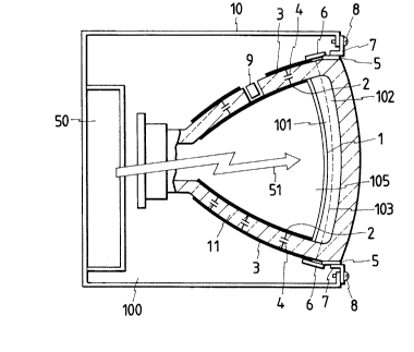
Fig. 1 is a side cross-sectional view of a CRT display
unit 100 according to the present invention, where a grounded
chassis 10 contains a video amplifier 50 for amplifying image
micro signals of rectangular wave forms and high frequencies
sent from a computer (not shown in the figure) to a large
amplitude. A CRT 105 and amplifier 50 are both solidly
fastened to the grounded chassis 10. CRT 105 comprises a
funnel section 101 (toward the video amplifier) and a panel
section 102, both glass-sealed at a joining section 103 shown
in a dotted line. On the external surface of the funnel
section 101 is deposited a conductive coating film 3 for
preventing a high surge voltage, and a conductive coating film
2 is deposited on the internal surface for introducing a high
voltage from an anode terminal 9 into the tube. Graphite is
normally used as conductive coating films 2 and 3. The
conductive coating film 2 is electrically connected to the
shadow mask 1, and the conductive coating films 2 and 3 are
also electrically connected through a coupling capacitor 4.
The circumference of panel section 102 is surrounded b~ a
metal rim band 5, and the rim band 5 and the conductive
coating film 3 are connected by a conductive member 6. The
rim band 5 is further connected electrically to the chassis 10
through conductive elastic bodies 7 and clamping screws 8.
Thereby, the shadow mask 1 is electrically connected to the
chassis 10 through elements 1-2-4-3-6-5-7-8-10.
Fig. 2 is a perspective view of the tube 105, where the
2~3828~
conductive member 6 referred to in Fig. 1 is realized, for
instance, by a tape with a lining coated with an adhesive,
which connects the conductive coating film 3 and the rim band
5 at a plurality of locations. As is clearly understandable
from Fig. 1, it is preferable for the conductive coating
member 6 to be arranged so that is not in direct contact with
the joining section 103 which joins the funnel section lOl and
the panel section 102. This is because the air tightness at
the joining section 103 is weaker than that at other locations
thereby necessitating that preventive measures be taken
against the deterioration of the hermetic insulation resulting
from application or the conductive coating film 3 or direct
contact with the conductive member 6. As another practical
means for installing the conductive member without
deteriorating the hermetic insulation, after applying a high
voltage insulation paper on the glass at the joining section
103, the conductive member of the present invention may be
installed thereon. In the case where the conductive member 6
is in the form of a tape as shown in Fig. 2, the tape should
be made of copper of aluminum with a width of 1-3 cm, and its
adhesive lining should also have a conductive property. In
this embodiment, two strips of conductive tape have been
applied to each of the four sides of the tube, the upper, the
bottom and the left and right sides of the tube. The tape,
needless to say, may take the form of plate.
Fig. 3 is a front elevational view of the CRT display
unit shown in Fig. 1, where the tube 105 is fastened to the
chassis lO by means of metal fixtures 30 formed together on
the rim band 5. With respect to the conductive elastic body 7
in Fig. 1, in fact, as shown in this embodiment, one end of
which is fastened, for example, to the chassis 10 by means of
fastening screws, and the other end is pressed in contact with
the rim band 5 by means of its resilient force. The
conductive elastic body 7 is a spring made of, for example,
phosphor bronze or stainless steel, with a length of several
cm, and has cushioning properties at both ends. In Fig. 3,
two conductive elastic bodies 7 are provided for each of the
2~382~1
upper and bottom sides of the tube. These bodies may also be
added to each of the left and right sides.
The number of installations of the above-described
conductive member 6 and conductive elastic body 7 may be
determined appropriately according to the levels and
frequencies of electromagnetic radiation leaking from the CRT
display equipment. It is found, however, according to the
results of our experiments pursuant to the present invention
that the reduction rate of electromagnetic radiation becomes
greater with an increasing number of installations of the
conductive elastic bodies 7.
As should be clearly understood from Figs. 1 and 3,
according to the present invention, the shadow mask 1 is
electrically connected to the chassis 10 by way of the shadow
mask 1, conductive coating film 2, coupling capacitor 4,
conductive coating film 3, conductive member 6, rim band 5,
conductive elastic body 7, fastening screw 8 and chassis 10,
thereby forming an electromagnetic shield plate of the shadow
mask. In fact, the electromagnetic radiation 51, shown
graphically in Fig. 1, is reduced substantially and is hardly
permitted to leak out of the front panel of the video
amplifier 50.
Fig. 4 illustrates how this embodiment of the present
invention has attained the regulation values set by the VCCI
and the FCC. In the figure, the X-axis indicates the
frequencies of electromagnetic radiation, while the y-axis
indicates levels of electromagnetic radiation detected at a
distance of 10 m from the source of electromagnetic radiation.
Shown in a solid line are the values of regulations set by the
VCCI, while shown in a dotted line are those set by the FCC.
The regulation values set by the VCCI are more stringent in
comparison with those set by the FCC. A characteristic (A) is
for the case of Japan Patent Laid-Open No. 58-7751 (1983),
where an externally clad graphite film 3 is extended as far as
the rim band 5, and is grounded by means of metal fixtures 30
installed on the four corners of the rim band to fasten the
same to the chassis. A characteristic (B) is for the case of
203~81
Japan Patent No. 62-267790 (1987), where a ground is provided
by grounding at one point on the rim band 5 portion and one in
the outer clad graphite portion, respectively.
Character (C) is for the case of an embodiment of the
present invention, where a rim band 5 and an outer clad
graphite film 3 are connected at a plurality of locations
through conductive members 6, and in addition, the rim band 5
and the chassis 10 are connected at a plurality of locations
through conductive elastic bodies 7. As is clear from this
figure, according to the present invention, the radiation
noise levels lower by 9dB than the regulation level are
attainable at 300MHz; lower by 6dB at 200MHz than the most
stringent VCCI standard; and lower by 4dB at lOOMHz than the
VCCI standards.
Actual reductions in the radiation noise levels, for
example, by 6dB, imply that, when evaluated in terms of
distance from the noise source, it has been reduced by half.
That is, in comparison with the standard CRT display unit
having a 40dB noise level at a distance of lOm from a noise
source at 200MHz frequency, a CRT display unit according to
the present invention is capable of being placed as near as 5m
from the noise source holding the noise level the same at a
40dB level, at 200MHz frequency. In other words, according to
the present invention, a required distance between a CRT
display unit and other electronic equipment susceptible to EMI
from the unit can be halved.
The advantages of the present invention as described
above have been attained by: forming a shield panel of the
shadow mask 1 by electrically connecting the shadow mask 1 in
a CRT tube with the rim band 5 and fastening the same to the
chassis 10 through metal fixtures 30; and also electrically
connecting the space between the rim band 5 and the chassis 10
with conductive members 7, thereby reducing radiation noise
leaking out of the space significantly. In Fig. 3, a
conductive elastic body was used as a conductive member 7.
However, there are other modifications of the present
invention. In Fig. 5, gasket 21 is inserted in the space
2~3~2~1
between a rim band 5 and chassis 10. The gasket 21 may be
attached either to the rim band 5 or to the chassis 10 before
the CRT is fastened to the chassis 10 by means of metal
fixtures 30. The gasket may also be inserted in the space
after the fastening has been completed. Further, as another
means for electrically connecting a conductive coating film 3
deposited on a CRT and a rim band 5, both may be covered by a
metal plate 22 as shown in Fig. 6. Otherwise, as described in
Japan Patent No. 58-7751 (1983), a conductive coating film
coated on the tube funnel section may be extended as far as
the rim band through which it is grounded. Still further, as
shown in an embodiment in Fig. 7, conductive members 6 are
arranged to be electrically connected to a conductive coated
film 3 and a rim band 5, and at the same time, for a
conductive elastic body 20 to be fastened at one end to
chassis 10, and press-contacted to the conductive coated film
3 at the other end.