Note: Descriptions are shown in the official language in which they were submitted.
2 ~) ~ 8 ~
HIGH SPEED FAIL PROCESSOR
sackaround of the Invention
The invention relates to fail processors.
It is known to generate patterns which are
used in automatic test equipment by providing a high
speed pattern generator which generates address
sequences which are sent to a pluxality of local
generator circuits. Each local generator circuit
includes a high speed local memory, a multiplicity
of timing generators, a multiplicity of corresponding
interpolators, a high speed formatter and a high
speed fail processor. The timing generatoxs and
interpolators run in an interleaved fashion, with one
timing generator/interpolator set receiving and gen-
erating all even cycle information and the other setreceiving and generating all odd information.
Summarv of the Invention
It has been discovered that providing a fail
processor which receives test data from a node and
generates failure data based upon the test data, a
plurality of fail memories, each memory being con-
figured to receive and store certain fail data, and
a sequence memory configured to store sequence infor-
ma~ion indicating in what order the failure data is
stored in the plurality of fail memories provides an
apparatus for processing failure information received
from a node of a circuit under test.
Descriution of the Preferre_ Embodiment
The attached drawings illustrate the
preferred embodiment, the structure and operation of
which is then described.
r ~ 2038~9~
Drawinas
Fig. 1 is a schematic-block diagram of a
test system according to the present invention.
Figs. 2-4 are examples of-how failure in-
S formation is stored in'the Fig. 1 test system.
Structure
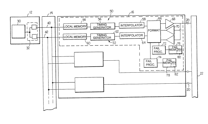
Referring to Fig. 1, test system 10 includes
pattern generato~ circuit 12, distribution circuit 14
and a plurality of local generator circuits,l6. Each
local generator circuit provides a signal at node 20 to
a circuit under test (CUT) 22.
Pattern generator circuit 12 includes con-
ventionally designed high speed pattern generator 30
which provides address patterns at a frequency of
122.0703125 MHz (generally, and hereinafter, ~eferred
to as "120 MHz", and its half as "60 MHz") and fre-
quency divider circuit 3Z which receives the high
frequency patte-rns generated by pattern generator 30
and provides a pair of lower fre~uency addresses
which are half the frequency (i.e., 60 MHz~ of the
high frequency addresses generated by pattern genera-
tor 30.
Distribution circuit 14 includes a pai_ of
signal distribution paths 40, 42. Each signal dis-
tribution path 40, 42 includeS a parallel-multibit
bus which simultaneously provides the lower frequency
address to a plurality of local generator circuitS 16.
Each local generator circuit 16 includes a
pair of signal generating circuits 50, 52. Signal
generating circuit 50 includes local memory 5~l, which
receivPs information ~rom distribution patA 40 and
provides a data output to timing generator 56, t mln~
generator 56 which receives the data out-u' ~nd
,. .
.1 ' .
r ~
3 ~ ~ 9 ~
-- 3
provides a timins generator output to interpolator
circuit 58. Likewise, signal path S2 includes local
memory 60, which receives information from distribu-
tion path 42, timing generator 62, which receives
information from locaL memory 60, and interpolator
circuit 64, which receives information from timing
generator 62.
Interpolator circuits 58 and 64 provide
signals to high speed fcrmatter 66. Formatter 66 is
a conventional emitter coupled logic (ECL) high speed
ormatter which receives timing pulses and data and
provides a two bit ~averorm indicating level and tri-
state at a particular time. Driver 68 receives these
signals, and provides an output to node 20 having the.
lS correct voltage levels and tri-state conditions for
the particular CUT.
Dual detector 70 is also connected to node
20; dual detector 70 receives signals from node 20
and provides an out2ut to high speed formatter 66.
High speed formatter 66 is also connected to a pair
o fail processors 72, 74. Fail processors 72, 74
include respective fail ~.emo-ies 76, 78. Each fail
memory 76, 78 includes se~uence memory portion 80, 82.
ODeration
Referriny to Fig. l, system lO both prcvides
signals to and detects infor~ation from node 20 of .
CUT. More specifically, when providing sisna1s to
node 20, pattern generator 30 generat_s add-ess
patterns at a frequency of 120 ~IHz. This in_e.,mati~n
30 is provided to ~requency dividr'r circui~ ' ~ w, -h
receives the 120 ~lHz address pattern and ~r^~ tJo
alternating cycles of half speed (i,e., 6G
.,
::
.
~382~
- 4 -
address patterns to signal distribution paths 40, 42,
respectively. Alternate cycles move respectively
ovex lines 40 and 42, even over the former and odd
over the latter; and successive cycles are
identifie d by their leading edges. Because the
pattern is frequency divided prior to transmission to
local generators 16, signal distribution paths 40,
42 need only be appropriate for transmitting signals
having a frequency of 60 M~lz rather than signals
having a frequency of 120 MHz.
At power-up and at the start-up ofeach
pattern burst, system 10 is resynchronized. More
specifically, frequency divider circuit 32 is con-
figured so that at power-up, as well as when it is
resynchronized, the ne~t signal provided by frequency
divider circuit 32 is over signal path 40.
Distribution circuit 14 provides the two
half speed address patterns generated by divider
circuit 32 to 512 channels. Each channel includes
a local generator circuit 16, as shown in Fig. lo
Each iocal generator circuit 16 provides
a high frequency signal to, and detects a high
frequency signal from, node 20. When detecting sig-
nals from node 20, dual detector receives the high
frequency signal and provides the high frequency
signal to formatter 66. Formatter 66 provides two
half speed signals to fail processors 72, 74; the
half speed signals correspond to the cycles o~ the
half speed address patterns. Fail processorS store
the failure information in fail memories 76, 78,
which function independently at half the speed or
~ ( 2 ~ 3 ~3 r~ 9 ~
formatter 66. Because fail memo~ies 76, 78 function
at half the speed of formatter 66, lower cost
memories may be used.
Information may be stored in fail memories
76, 78 in one of three modes of operation. In a store
all (Store All) mode, failure information is continu-
ally, alternately written into successiYe locations
of fail memories 76, 78. Fig. 2 shows an example of
how the failure information is stored in the Store
All mode. In a store this vector (STV) mode, failure
information is selectively written into the fail mem-
ories based upon the value of a vector bit. In a
store only fail (SOF) mode, failure information is
written into fail memories 76, 78 on cycles which
contain a fail. Or, there may be chosen a combined
STV and SOF mode. Fig. 3 sho-~Js an example of how
the failure in~ormation is stored in fail memories
76, 78 for the STV mode and the SOF mode. It is
apparent from Fig. 3 that in the STV mode and the SOF
mode the failure information is stored in the fail
memory which corresponds to the cycle in which the
information was generated. Accordingly, to recon-
struct ~he sequence in which the ~ailure information
was stored in fail memories 76, 78 further information
is necessary.
In order to reconstruct the failure infor-
mation storage sequence, fail memories 76, 78 use
respective sequence memory portions 80, 82. Pig.~l
shows an example of how the failure and sequence in-
formation is stored in fail memories 76, 78 and
`, ~ ',, '
. , : ; .
;:
'' ~ ,,
r r 2 ~
sequence memory portions 80, 82. Sequence memoryportions 80, 82 allow the failure information storage
sequence to be reconstructed by trac~in~ the lailure
information as the information is stored. More
~pecifically, a low is stored in a respective
sequence memory portion if the previous write was
in the same path. A high is stored in a respective
sequence memory portion if the previous write was in
the other path. By using this information, the
failure information storage sequence can be easily
reconstructed.
Other Embodi~ents
Fail processors 72, 74 may be connected
to a common sequence memory. By cent-ally storing
the sequence information, the fail memori~s may
operate independently. Add tionalL~, because the
se~uence information is centrally stored, fail mem-
ories 72, 74 may be distributed without providing local
means for determining the secuence of stored bits.
Additionally, while the preferred embodimen~
includes two signal generatlon paths, the system l~ay
operate with one signal generation path but a
plur21ity of fail processors. In such a system, the
failure information may be stored at a lower ~requenc~
than the generated patterns.
Additionally, while the ~referrcd embodiment
includes two fail prccessor~ and two fail memorieS,
the system may ~lso operate with one fail prcc2ssOr
and t~,/o fail memorIes. In 5uch a system, the .-ailu-e
infor~ation may be stored at a lower fr ~a~e.~~, t~._n
th2t at which the fail processor operatcs.
. ., : . : :. : .
,
~ '
, :
;
. . ' , . . .
2~38295
Additionally, while the preferred embodiment
shows two fall memories, the number of fail memories
may be lncrease~ simply by providin~ more bits to a
sequence memory; the bits indicate where in which
memory previous write is located.
~ ~ .
,
:
:: :
:~
.
~: :