Note: Descriptions are shown in the official language in which they were submitted.
- 1 - 2~3~359
l Liquid Crystal Device, and Display Method and
Display System Making Use of It
BACKGROUND OF THE INVENTION
5 Field of the Invention
The present invention relates to a liquid
crystal device used in a liquid crystal display
device, a liquid crystal optical shutter or the like.
More particularly the present invention is concerned
10 with a liquid crystal device having achieved an
improvement of alignment characteristics of liquid
crystal molecules, and a display system in which such
a liquid crystal device is used for display.
Related Background Art
Clark and Lagerwall have proposed a display
device of the type the refractive index anisotropy of
ferroelectric liquid crystal molecules is utilized and
transmitted light rays are controlled by its
combination with a polarizer (see Japanese Patent
20 Application Laid-open No. 56-107216 and U.S. Patent
No. 4,367,924). This ferroelectric liquid crystal
commonly has a chiral smectic C phase (Sm*C) or H
phase (Sm*H) of non-spiral structure in a specific
temperature range, and, under such a state, has the
25 properties of assuming either a first optically stable
state or a second optically stable state in response
203~3~9
-- 2 --
l to an electric field applied and also maintaining that
state when no electric field is applied, in other
words, the bistable state (or two stable states).
This ferroelectric liquid crystal also has a quick
5 response to changes in electric fields, and is
expected to be widely utilizable as a display device
of a high-speed and memory type. In particular, in
view of its function, it is expected applicable as a
display device with a large screen and high
10 resolution.
In order for an optical modulation device
making use of such a bistable liquid crystal to
exhibit drive characteristics, a liquid crystal
disposed between a pair of parallel substrates is
15 required to be in the state of molecular orientation
that the conversion between the above two stable
states may effectively take place.
In the case of a liquid crystal device in
which the double refraction of a liquid crystal is
20 utilized, the transmittance under cross polarization
is expressed by:
~nd
I/Io = sin 4~ sin A
203~369
- 3 -
1 wherein Io incident light intensity,
I: transmitted light intensity,
~: tilt angle
~n: refractive index anisotropy
d: film thickness of a liquid crystal layer,
A: wavelength of incident light.
Thus, the tilt angle ~ in the above non-spiral
structure is present as an angle in the direction of
an average molecular axis of liquid crystal molecules
10 twistingly oriented in the first and second states of
alignment. According to the above expression, the
transmittance reaches a maximum when the tilt angle
is at an angle of 22.5, and hence a tilt angle ~ in
the non-spiral structure that effects the bistable
15 state is required to be as near as possible to 22.5.
Incidentally, as a method of aligning
ferroelectric liquid crystal, a liquid crystal
molecular layer formed of a plurality of molecules
that form a smectic liquid crystal over a large area
20 must be monoaxially aligned along its normal and hence
a polyimide film usually having been subjected to
rubbing has been widely used. In particular, the
method as disclosed, for example, in U.S. Patent No.
4,561,~26 is known as a method of aligning a chiral
25 smectic liquid crystal of non-spiral structure.
However, in instances in which hitherto available
'~ 2o38369
alignment methods using a polyimide film having been
subjected to rubbing are applied to the above bistable
ferroelectric liquid crystal of non-spiral structure as
reported by Clark and Lagerwall, there are the following
problems.
That is to say, experiments made by the present
inventors revealed that a tilt angle ~ (as described later)
in a ferroelectric liquid crystal of non-spiral structure
obtained by making alignment using the conventional
polyimide film having been subjected to rubbing becomes
smaller than a tilt angle O (the angle of 1/2 of a vertical
angle of a trigonal pyramid, (as described later) in a
ferroelectric liquid crystal of spiral structure. In
particular, the tilt angle ~ in a ferroelectric liquid
crystal of non-spiral structure obtained by making
alignment using the conventional polyimide film having been
subjected to rubbing was approximately 3 to 8 in general,
and the transmittance at that time was approximately 3 to
5 ~ at best.
Thus, according to Clark and Lagerwall, the tilt angle
in a ferroelectric liquid crystal of non-spiral structure
that effects the bistable state should be the same angle as
the tilt angle in a ferroelectric liquid crystal of spiral
structure. In
2038369
_ 5
practice, however, the tilt angle ~ in the non-spiral
structure is smaller than the tilt angle 0 in the spiral
structure. It was also revealed that the reason why the
tilt angle ~ in the non-spiral structure is smaller than
the tilt angle 0 in the spiral structure is ascribable to
the twisted orientation of liquid crystal molecules in the
non-spiral structure. More specifically, in the
ferroelectric liquid crystal of non-spiral structure,
liquid crystal molecules are twistingly oriented in a
continuous form at a twist angle ~, which is twisted from
an axis of a liquid crystal molecule adjacent to an upper
substrate toward an axis of a liquid crystal molecule
adjacent to a lower substrate (i.e., in the direction of
twisted orientation), with respect to the normal of each
substrate. This is the reason why the tilt angle ~ in the
non-spiral structure becomes smaller than the tilt angle
in the spiral structure.
In the instance where a chiral smectic liquid crystal
is aligned using a conventional polyimide alignment film
having been subjected to rubbing, the polyimide alignment
film is present as an insulating
2 1~ 5 ~
- 6 -
l layer between an electrode and a liquid crystal layer.
Hence, when a voltage with one polarity is applied so
that the first optically stable state (for example, a
state of the display in white) is switched to the
5 second optically stable state (for example, a state of
the display in black), a reverse electric field Vrev
with the other polarity is produced in a ferroelectric
liquid crystal layer after removal of the application
of this voltage with one polarity, and this reverse
10 electric field Vrev has often caused an after-image at
the time of display. (see, Yoshida Akio, "Switching
Characteristics of SSFLC", Proceedings for Liquid
Crystal Forum, p.142-143, October, 1987.
15 SUMMARY OF THE INVENTION
The present invention was made in order to
solve the problems involved in the prior art. In
particular, an object of the present invention is to
provide a liquid crystal device having a chiral
20 smectic phase, and a display system, that can produce
a large tilt angle ~ in the non-spiral structure of a
chiral smectic liquid crystal, enables display of an
image with a high contrast, and also can achieve
display that may cause no after-image.
The present invention provides a liquid
crystal device comprising a pair of opposing
2~3~3S~
- 7 -
l substrates and a liquid crystal rendering a chiral
smectic phase, disposed between said pair of
substrates, wherein at least one of said substrate is
provided with an alignment film comprising a polymer
5 containing a skeleton selected from the group
consisting of acetylene, phenylene, phenylenevinylene,
phenylenexylidene, benzyl, phenylene sulfide,
dimethylparaphenylene sulfide, thienylene, furan,
selenophene, vinylpyridine, vinylnaphthalene,
10 vinylferrocene, vinylcarbazole, phenylene oxide,
phenylene selenide, heptadiyne, benzothiophene,
thiophene, pyrrole, aniline and naphthylene. The
present invention also provides a display system
comprising such a liquid crystal device.
BRIEF DESCRIPTION OF THE DRAWINGS
Fig. 1 is a diagrammatic illustration of a
ferroelectric liquid crystal device according to the
present invention.
Fig. 2 is a perspective illustration of a
state of alignment of a chiral smectic liquid crystal
of spiral structure
Fig. 3 is a perspective illustration of a
state of alignment of a chiral smectic liquid crystal
25 of non-spiral structure.
Fig. 4 is an illustration of the relationship
203836~
1 between a monoaxial alignment axis of substrates and
an axis of a ferroelectric liquid crystal molecule of
non-spiral structure.
Fig. 5 is a cross-sectional illustration of a
5 state of alignment of a chiral smectic liquid crystal
aligned according to an aligning method of the present
invention, Fig. 6 illustrates C-directors of its state
of uniform alignment, and Fig. 7 illustrates C-
directors of a state of spray alignment.
Fig. 8A is a view to illustrate a tilt angle
in the state of uniform alignment, and Fig. 8B is a
view to illustrate a tilt angle O in the state of
spray alignment.
Fig. 9 shows a progressive series of cross-
15 sectional illustrations of the distribution of
electric charges in a ferroelectric liquid crystal,
the direction of spontaneous polarization Ps and the
direction of a reverse electric field Vrev,
respectively.
Fig. 10 is a view to illustrate changes of the
tilt angle ~ at the time of application of an electric
field and after that time.
Fig. 11 is a graph to show optical response
characteristics in a liquid crystal device of the
25 prior art, and Fig. 12 is a graph to show opticalresponse characteristics in a liquid crystal device of
21j~3~9
l the present invention.
Fig. 13 illustrates wave forms of a drive
voltage used in Examples of the present invention.
Fig. 14 is a diagrammatic illustration of
5 another ferroelectric liquid crystal device according
to the present invention.
Fig. 15 is a cross-sectional illustration of
an FET in a TFT used in the present invention.
Fig. 16 is a cross-sectional illustration of a
10 ferroelectric liquid crystal device cell in which the
TFT is used.
Fig. 17 is a perspective illustration of a TFT
substrate.
Fig. 18 is a plan view of the TFT substrate.
Fig. 19 is a partial cross-sectional view
along the line A-A' in Fig. 18, and Fig. 20 is a
partial cross-sectional view along the line B-B' in
Fig. 18.
Figs. 21 and 22 illustrate a liquid crystal
20 display system having a communication synchronizing
means.
DESCRIPTION OF THE PREFERRED EMBODIMENTS
Fig. 1 diagramatically illustrates a
25 ferroelectric liquid crystal device according to the
present invention. In Fig. 1, the numerals lla and
2~3836~
- 10 -
l llb denote glass substrates covered with transparent
electrodes 12a and 12b made of In203, IT0 (indium-tin
oxide) or the like, respectively. Insulating films
13a and 13b (e.g., SiO2 films, TiO2 films, Ta205
5 films) of 200 to 1,000 A thick and alignment films 14a
and 14b formed of the polymer described above are
laminated thereon, respectively. A liquid crystal 15
rendering a chiral smectic phase is disposed between
the alignment films 14a and 14b. The distance between
10 them is set to be a distance (for example, 0.1 ~m to 3
~m) small enough to control the formation of a spiral
structure of the chiral smectic liquid crystal 15.
The liquid crystal 15 rendering the chiral smectic
phase has produced a bistably aligned state. The
15 above small enough distance between which the chiral
smectic liquid crystal 15 is disposed is retained
using a beads spacer 16 (e.g., silica beads, alumina
beads) disposed between the alignment films 14a and
14b. The numerals 17a and 17b denote polarizing
20 plates.
The alignment films used in the present
invention can be formed by the conventionally known
Langmuir-Brodgett process, vacuum deposition or
coating to give a monomolecular built-up film, a
25 deposited film or a coating film.
In the case when the alignment film is formed
2~3S~
11 -
l by the Langmuir-Brodgett process, the film thickness
should be controlled to be approximately from 4 A to
80 A, and preferably from 16 A to 32 A. With regard
to the direction in which a substrate is drawn up when
5 the alignment film is formed, the film should be
formed in such a manner that the drawn-up directions
for the upper and lower substrates may be the same
directions when they are framed into a cell (e.g., the
directions A shown in Fig. 1).
The alignment film formed by vacuum deposition
or coating should have a film thickness of usually
from 50 A to 2,000 A, and preferably from 100 A to 200
A.
To form the alignment film, a film comprised
15 of a polymer is used, which polymer may preferably
comprise a polymer containing at least one skeleton
selected from acetylene, phenylene, phenylenevinylene,
phenylenexylidene, benzyl, phenylene sulfide,
dimethylparaphenylene sulfide, thienylene, furan,
20 selenophene, vinylpyridine, vinylnaphthalene,
vinylferrocene, vinylcarbazole, phenylene oxide,
phenylene selenide, heptadiyne, benzothiophene,
thiophene, pyrrole, aniline and naphthylene.
Stated specifically, such a polymer may
25 preferably include polyacetylene, polydiacetylene,
polyparaphenylene, polymethaphenylene,
2~3~6~
- 12 -
l polyparaphenylenevinylene, polyparaphenylenexylidene,
polybenzyl, polyparaphenylene sulfide,
polydimethylparaphenylene sulfide, polythienylene,
polyfuran, polyselenophene, poly-2-vinylpyridine, poly-
5 1-vinylnaphthalene, poly-2-vinylnaphthalene,
polyvinylferrocene, poly-N-vinylcarbazole,
polyparaphenylene oxide, polyparaphenylene selenide,
poly-1,6-heptadiyne, polybenzothiophene,
polythiophene, polypyrrole, polyaniline and
10 polynaphthylene-
The polymer of the present invention may
further have a substituent so long as it has the key
skeleton described above. Such a substituent
includes, for example, the following:
-~-CH2 ~ c 3
( CH2~0H
( 2 ~ 2
-O ( CH2~CH3
(wherein n represents an integer of 0 to 10)
In the case when the organic film (alignment
film) is formed as a monomolecular built-up film, the
polymer should particularly preferably have the
substituents -~-CH2 ~ 3 and ( CH2 )n C02H in
combination.
From the viewpoint of more satisfactory
prevention of the after-image ascribable to a reverse
2 ~ J
- 13 -
1 electric field, the organic film of the present
invention should preferably be formed of a film so
polymerized that it is made conductive to have a
conductivity greater than 10 8 Q cm
The substrate on which the alignment film
comprising the above polymer is used in both of a pair
of opposing substrates or one of the substrates.
Liquid crystal materials used in the present
invention may preferably be liquid crystals that
lO produce a chiral smectic C phase through an isotropic
phase, a cholesteric phase, and a smectic A phase in
the course of temperature drop. Particularly
preferred is a liquid crystal having a pitch of not
less than 0.8 ~m when it is in a cholesteric phase
(the pitch in a cholesteric phase is measured at the
middle in the temperature range of the cholesteric
phase). Preferably usable specific liquid crystal
materials are liquid crystal compositions incorporated
with the following liquid crystal materials "LC-1",
20 "80B'l and "80SI*" in the following proportions.
2~3~69
- 14 -
L C -- 1
O CH3
CsH~O ~ CO ~ OCH2CHC2Hs
8 0 B
CH3 O
C2HsCHCH2 ~ CO ~ OCsH~ 7
8 O S I -
O CH3
CsH~ 70~ CO~ CHzCHC2Hs
Liquid crystal
(1) (LC-l)go/(80B)lo
(2) (LC-1)30/(80B)zo
(3) (LC-1)70/(80B)30
(4) (LC-1)6o/(80B)40
(5) 80SI*
(In the above, the mixing proportions are each
expressed in weight ratio.)
Fig. 2 is a diagramatical drawing of an
example of a cell, to illustrate the operation that
has utilized ferroelectric properties of the liquid
25 crystal rendering a chiral smectic phase. The
numerals 2la and 2lb each denote a substrate (a glass
20383~
- 15 -
l plate) covered with a transparent electrode comprised
of a thin film made of In2O2, SnO2, ITO or the like.
Between the substrates, a liquid crystal of an SmC*
(chiral smectic C) phase or an SmH* (chiral smectic H)
5 phase is sealed, which is so aligned that its liquid
crystal molecular layer 22 may be perpendicular to the
glass substrate surfaces. A line 23 shown by a thick
line indicates a liquid crystal molecule. This liquid
crystal molecule 23 has a dipole moment (Pl) 24 in the
10 direction falling at right angles with its molecule.
The angle that forms here a vertical angle of a
trigonal pyramid indicates the tilt angle ~ in the
chiral smectic phase of such spiral structure. When a
voltage higher than a given threshold value is applied
15 between the electrodes provided on the substrates 21a
and 21b, the spiral structure of the liquid crystal
molecule 23 comes loose, and thus the liquid crystal
molecule 23 can change its direction of alignment so
that all of dipole moments (Pl) 24 face toward the
20 direction of the electric field. The liquid crystal
molecule 23 has a slender shape, and shows refractive
index anisotropy between its direction of the major
axis and direction of the minor axis. Hence, it can
be easily understood that if, for example, polarizers
25 which are in crossed nicols each other are placed on
the glass substrate surfaces, there can be provided a
2 ~
- 16 -
l liquid crystal optical modulation device capable of
changing optical characteristics depending on the
polarity of the applied voltage.
A surface stable type ferroelectric liquid
5 crystal cell in the state of bistable alignment, which
is used in the liquid crystal device of the present
invention, can be made to have a sufficiently small
thickness, for example, of from 0.1 ,um to 3 ~m. As
the thickness of a liquid crystal layer becomes
10 smaller in this way, the spiral structure of liquid
crystal molecules comes loose even in the state where
no electric field is applied, and turns to have a non-
spiral structure, so that its dipole moment Pa or Pb
results in either an upward state (34a) or a downward
15 state (34b), as shown in Fig. 3. The numeral 32
denotes a perpendicular layer. When as shown in Fig.
3 an electric field Ea or Eb of a voltage higher than
a given threshold value and having a different
polarity is applied to such a cell through means of
20 applying a voltage (31a) and (31b), the dipole moment
changes its direction to an upward direction 34a or a
downward direction 34b corresponding to the electric
field vector of the electric field Ea or Eb, and,
corresponding therewith, the liquid crystal molecule
25 are aligned in the direction of either a first stable
state 33a or a second stable state 33b. The half
2038369
- 17 -
(1/2) of the angle formed here by the first and second
stable states corresponds to the tilt angle e.
The tilt angle e in the non-spiral structure is
smaller than the tilt angle ~ in the spiral structure
because of the twisted orientation of liquid crystal
molecules in the non-spiral structure. More specifically,
in ferroelectric liquid crystal of non-spiral structure,
liquid crystal molecules are, as shown in Fig. 4,
twistingly oriented in a continuous form at a twist angle
~, which is twisted from an axis 42 of a liquid crystal
molecule adjacent to an upper substrate toward an axis 43
of a liquid crystal molecule adjacent to a lower substrate
(i.e., in the direction 44 of twisted orientation), with
respect to the normal of each substrate. In Fig. 4, the
numeral 41 denotes a monoaxial alignment axis formed on
upper and lower substrates, obtained by rubbing or oblique
vacuum deposition.
The effects obtainable from the ferroelectric
liquid crystal cell described above are firstly that the
response speed is very high, and secondly that the
alignment of the liquid crystal molecules is bistable. The
second effect will be further described with reference to,
for example, Fig. 3. When the electric field Ea is
applied, the liquid crystal molecules are aligned in the
first stable state 33a and this state is stable even when
the electric field has been removed. On the other hand,
when the electric field Eb of a reverse direction is
,~.
- 17A - 2 0 3 8 3 6 9
applied, the liquid crystal molecules are aligned in the
second stable state 33b to change their direction, and
still remain in this state even when the electric field has
been removed. The respective states of alignment are also
maintained so long as the electric field Ea to be applied
does not exceed a given threshold value.
Fig. 5 is a cross-sectional view diagrammatically
explaining the state of alignment of liquid crystal
molecules as produced by the method of alignment using the
alignment film in the liquid crystal device according to
the present invention. Fig. 6 illustrates the C-directors
thereof.
The numerals 51a and 51b shown in Fig. 5
_, . _ . . .
20~3~
- 18 -
l denote an upper substrate and a lower substrate,
respectively. The numeral 50 denotes a li~uid crystal
molecular layer formed of liquid crystal molecules 52,
and the liquid crystal molecules 52 are arranged with
5 changes in their positions along the base 54
(circular) of a cone 53.
Fig. 6 illustrates C-directors. U1 in Fig. 6
shows C-directors 63 which are in one state of stable
alignment, and U2, C-directors 63 which are the other
10 state of stable alignment. Each C-director 63 is a
projection of a molecular major axis on an imaginary
face perpendicular to the normal of the liquid crystal
molecular layer 50 shown in Fig. 5.
On the other hand, Fig. 7 shows the state of
15 alignment as produced using a conventional polyamide
film having been subjected to rubbing. For the state
of alignment as shown in Fig. 7, the molecular axis is
so largely twisted from the upper substrate 51a toward
the lower substrate 51b that the tilt angle ~ is
20 small.
Fig. 8A is a view to show the tilt angle
when the C-directors 63 are in the state of Fig. 6
(herein called "the state of uniform alignment"), and
Fig. 8B is a view to show the tilt angle ~ when the C-
25 directors 63 are in the state of Fig. 7 (herein called"the state of spray alignment"). In Figs. 8A and 8B,
203~S9
- 19 -
l the numeral 60 denotes the direction in which a
substrate is drawn up when the alignment film is
formed by the Langmuir-Brodgett process, or the axis
of rubbing treatment applied to the alignment film
5 formed by vacuum deposition or coating. The numeral
61a denotes an average molecular axis formed in the
state of alignment U1; 61b, an average molecular axis
formed in the state of alignment U2; 62a, an average
molecular axis formed in the state of alignment S1;
10 and 6Zb, an average molecular axis formed in the state
of alignment S2. The average molecular axes 6la and
61b can be converted by applying a voltage of reverse
polarity which exceeds a threshold voltage each other.
The same may also takes place between the average
15 molecular axes 62a and 62b.
Usefulness of the state of uniform alignment
to the delay of optical response (after-image) caused
by a reverse electric field Vrev will be explained
below. When the capacity of an insulating layer
20 (alignment control film) of a liquid crystal cell is
represented by Ci, the capacity of a liquid crystal
layer by CLc, and the spontaneous polarization of a
liquid crystal by Ps, the Vrev that causes the after-
image is represented by the following expression:
rev 2 Ps / Ci + CLC
Fig. 9 shows cross-sectional views to
203~3fi9
- 20 -
l diagrammatically illustrate the distribution of
electric charges in a liquid crystal, the direction of
spontaneous polarization Ps, and the direction of a
reverse electric field Vrev, respectively. Fig. 9(a)
5 shows the state of distribution of plus and minus
electric charges in a memory state before application
of a pulse electric field. At this time, the
spontaneous polarization Ps is in the direction from
the plus electric charges to the minus electric
10 charges. Fig. 9(b~ shows the direction of the
spontaneous polarization Ps immediately after removal
of the pulse electric field, where the spontaneous
polarization Ps is in a reverse direction to the
direction in the state shown in Fig. 9(a) (hence, the
15 liquid crystal molecules are reversed from the one
state of stable alignment to the other state of stable
alignment). Since, however, the state of distribution
of plus and minus electric charges is the same as in
the state shown in Fig. 9(a), a reverse electric field
20 Vrev is produced in the liquid crystal in the
direction of an arrow B. This reverse electric field
Vrev disappears after a while as shown in Fig. 9(c),
and the state of distribution of plus and minus
electric charges is changed.
Fig. 10 illustrates changes of optical
response occurring in the state of spray alignment as
~ ~ 3 ~
- 21 -
l produced using a conventional polyimide alignment
film, which are converted to changes of the tilt angle
. As shown in Fig. 10, when a pulse electric field
is applied, the molecular axis is overshot from the
5 average molecular axis S(A) formed in the state of
spray alignment to the average molecular axis U2
formed in the state of uniform alignment, which is in
the vicinity of the maximum tilt angle ~, along the
direction of an arrow X1. Immediately after removal
10 of the pulse electric field, the reverse electric
field Vrev as shown in Fig. 9(b) acts, and the tilt
angle ~ is decreased, along the direction of an arrow
X2, to the average molecular axis S(B) formed in the
state of spray alignment. Then, a state of stable
15 alignment can be obtained in which, because of the
action of attenuation of the reverse electric field
Vrev as shown in Fig. 9(c), the tilt angle ~ has been
a little increased, along the direction of an arrow
X3, to the average molecular axis S(C) formed in the
20 state of spray alignment. Fig. 11 is a graph to show
a state of optical response obtained here.
According to the present invention, employment
of the alignment film of the present invention does
not bring about such a state of alignment of a liquid
25 crystal that the average molecular axes S(A), S(B) and
S(C) are formed in the state of spray alignment as
~B383~
1 shown in Fig. 10, and hence makes it possible to align
a liquid crystal to form an average molecular axis
that may give a tilt angle ~ approximate to the
maximum tilt angle H.
Fig. 12 is a graph to show a state of optical
response obtained when the alignment film of the
present invention is used. As is seen from Fig. 12,
no delay of optical response caused by the after-image
occurs and also a high contrast is produced in a
10 memory state.
In the liquid crystal device of the present
invention, employment of the aligning method of a
specific type as will be made clearer in the following
Examples has achieved a state of alignment that gives
15 a high optical contrast between a light state and a
dark state, in particular, gives a high contrast to
unselected picture elements at the time of the
multiplexing drive as disclosed in U.S. Patent No.
4,655,561, etc., and also, with utilization of the
20 aspect that the alignment film comprises a conductive
polymer, brings about no delay in optical response at
the time of switching (at the time of multiplexing
drive), which may cause the after-image at the time of
display.
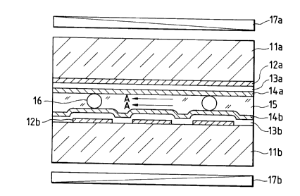
Fig. 14 diagrammatically illustrates another
liquid crystal device according to the present
2038359
- 23 -
l invention. The numerals denote the same as those
previously set forth with reference to Fig. 1.
Fig. 15 cross-sectionally illustrates an FET
(field effect transistor) in a TFT (thin film
5 transistor) used in the present invention. Fig. 16
cross-sectionally illustrates a ferroelectric liquid
crystal cell in which the TFT is used. Fig. 17
perspectively illustrates a TFT substrate. Fig. 18 is
a plan view of the TFT substrate. Fig. 19 is a
10 partial cross-sectional view along the line A-A' in
Fig. 18, and Fig. 20 is a partial cross-sectional view
along the line B-B' in Fig. 18. All the above
drawings (Figs. 15 to 20) illustrate an embodiment of
the present invention.
lS Fig. 16 shows an example of the liquid crystal
device provided with the alignment film of the present
invention. The device comprises a substrate llb made
of glass, plastic or the like and, formed thereon, a
semiconductor film 78 formed interposing a gate
20 electrode 82 and an insulating film 88, a TFT
comprised of two terminals 71 and 74 coming in contact
with this semiconductor film 78, and a picture element
electrode 75 (IT0, indium tin oxide) connected with
the terminal 74 of the TFT. An alignment film 14b and
25 also a light-screening film 72 made of aluminum,
chromium or the like are further provided thereon. An
20~369
- 24 -
l opposing electrode 81 (IT0, indium tin oxide) and an
alignment film 14a are formed on a substrate lla that
serves as an opposing substrate.
A liquid crystal 15, which is the liquid
5 crystal rendering a chiral smectic phase as previously
described, is held between these substrates lla and
llb. A sealing material 83 that seals the chiral
smectic liquid crystal 15 is provided on the periphery
of these substrates lla and llb.
Polarizers 17a and 17b in the state of crossed
nicols are disposed on both sides of the liquid
crystal device of such a cell structure. A reflective
plate 80 (an irregularly reflective aluminum sheet or
plate) is provided on the back of the polarizer 17a so
15 that an observer can view the state of display through
reflected light I1 of incident light Io~
In Figs. 15 to 20, the reference numerals
denote as follows:
71, a source electrode (a drain electrode);
20 72, a light-screening film;
73, an n layer;
74, a drain electrode (a source electrode);
75, a picture element electrode;
76, a substrate;
25 77, a light-screening film right beneath a
semiconductor;
- 25 - 2038369
l 78, a semiconductor;
79, a transparent electrode at a gate-wired portion;
80, a reflective plate;
81, an opposing electrode;
5 82, a gate electrode;
83, a sealing material;
84, a thin-film semiconductor;
85, gate wiring;
86, a panel substrate;
10 87, a gate having a light-screening effect; and
88, an insulating layer.
In the above drawings, the source electrode
and the drain electrode are referred to as those
limited to instances in which electric currents flow
15 from the drain to the source. Also possible is an
instance in which the source acts as the drain
depending on the action of the FET.
A liquid crystal display system can be set up
by employing the liquid crystal device of the present
20 invention at a display panel and providing a
communication synchronizing means as shown in Figs. 21
and 22 that operates according to an image information
data format having scanning line address information,
and SYNC signals.
In Figs. 21 and 22, the reference numerals and
symbols denote as follows:
2~3~3~
- 26 -
l 101, a ferroelectric liquid crystal display system;
102, a graphics controller;
103, a display panel;
104, a scanning line drive circuit;
5 105, an information line drive circuit;
106, a decoder;
107, a scanning signal generating circuit;
108, a shift register;
109, a line memory;
10 110, an information signal generating circuit;
111, a drive control circuit;
112, GCPU
113, a host CPU;
114, VRAM;
15 HB, host bus
DI, display information;
SLAI, scanning line address information;
DL, a data line;
TC, a transfer clock; and
20 HSP, a horizontal scanning period.
Image information is generated by means of the
graphics controller 102 provided on the main system
side, and transferred to the display panel 103 through
the signal transfer means shown in Figs. 21 and 22.
25 The graphics controller 102 governs the management and
communication of image information between the host
2~3~3~
- 27 -
l CPU (host central processing unit, HCPU in the
drawing) 113 and the liquid crystal display system
101, using the CPU (central processing unit, GCPU in
the drawing) and the VRAM (video random access memory)
5 114 as main units. The controlling in the present
invention is mainly carried out on this graphics
controller 102. Further, a light source is provided
on the backside of the display panel.
lO EXAMPLES
The present invention will be described below
in greater detail by giving Examples.
Example 1
Two sheets of 1.1 mm thick glass plate each
15 provided with a 1,500 A thick IT0 film and a 600 A
thick Ta205 film formed thereon were prepared as
substrates. The respective substrates were cleaned by
ultrasonic cleaning using isopropyl alcohol and then
left to stand for 24 hours in saturated vapor of
20 hexamethyldisilazane (HMDS) to carry out hydrophobic
treatment. Subsequently, on each substrate thus
treated, a conductive polymeric alignment film was
formed using the Langmuir-Brodgett process. The
process of forming the alignment film was as detailed
25 below.
An aqueous solution of 20 mol/lit. of a
2~3~
- 28 -
1 polymeric sulfonium salt represented by the formula
(2) obtained by condensation polymerization of p-
xylylene represented by the formula (1), carried out
in an aqueous alkali solution, was diluted to 1/10
5 with ethanol, and further diluted to a concentration
of 1 mol/lit. with 1,1,1-trichloroethane. Next, this
dilute solution was mixed with a solution of sodium
perfluorononanate, previously prepared in a
concentration of 1 mol/lit. using a 1:1 mixed solvent
10 of ethanol and 1,1,1-trichloroethane. A polymeric
compound represented by the formula (3) was thus
obtained, which was used as a spread solution.
Next, the resulting solution was spread over
pure water of 20C in water temperature to form a
15 monomolecular film on the water surface. After
evaporation of the solvent, the surface pressure of
the monomolecular film formed was increased to 25
mN/m. While keeping constant the surface pressure,
the substrate was vertically immersed and drawn up at
20 a rate of 10 mm/min to effect build-up of an eight-
layer Y-type monomolecular film on the substrate.
This substrate on which the polymeric
sulfonium salt had been built up was treated at 200C
for 2 hours under reduced pressure (about 1 Torr),
25 thereby converting the built-up film into the poly(p-
phenylenevinylene) represented by the formula (4) to
20383S9
- 29 -
l give an alignment film.
Thereafter, alumina beads with an average
particle diameter of about 1.5 ~m were sprayed on one
of the glass substrates. Then, the two sheets of
5 glass substrates were put together in such a way that
the axes of the directions in which the respective
substrates were drawn up were in parallel and in the
same direction each other. A liquid crystal cell was
thus fabricated.
Into the resulting cell, a ferroelectric
smectic liquid crystal "CS-1014" (trade name; a
product of Chisso Corporation) was vacuum-injected in
the state of an isotropic phase, and then cooled to
30C at a rate of 0.5C/hr from the state of the
15 isotropic phase. Thus, it was possible to align the
liquid crystal. In the cell of the present Example in
which this "CS-1014" was used, the phase changes
occurred as follows:
80.5C 69.1C 50C
20 Iso ~ Ch ) SmA ~ SmC*
(Iso: isotropic phase, Ch: cholesteric phase, SmA:
smectic A phase, SmC*: chiral smectic C phase)
The above liquid crystal cell was inserted
between a pair of 90 crossed nicols polarizers.
25 Thereafter, a 30 V pulse for 50 ,usec was applied
thereto and then the 90 crossed nicols were set to
2~3~3~9
- 30 -
l the position of extinction (a darkest state).
Transmittance at this time was measured using a
photomultiplier. Subsequently, a -30 V pulse for 50
~sec was applied, and transmittance at this time (a
5 bright state) was measured in the same manner. As a
result, it was revealed that the tilt angle ~ was 15,
the transmittance in the darkest state was 0.9 %, and
on the other hand the transmittance in the bright
state was 45 %. Hence the ratio of contrast was 50:1.
10 The delay in optical response that causes an after-
image was 0.2 second or less.
Using this liquid crystal cell, display was
carried out according to multiplexing drive in which
the drive wave forms as shown in Fig. 13 were used.
15 As a result, a display with a high contrast and high
grade was obtained. After an image was displayed by
inputting given characters, the whole screen was
turned off to a white state to confirm that no after-
image was seen to have occurred. The letter symbols
20 SN~ SN+1 and SN+2 in Fig. 13 represent wave forms of
the voltages applied to scanning lines. The letter
symbol I represents a wave form of the voltage applied
to a typical information line. I-SN is a synthetic
wave form of the voltage applied to the crossing area
25 of the information line I and the scanning line SN.
In the present Example, experiments were made under
2~3~3B9
- 31 -
l conditions of V0 = 5 V to 8 V and ~T = 20 ~sec to '170
~sec.
Et2S~CHz ~ CH2S~Etz ( 1 )
s 2CQ-
- H H
C- C ~ ( 2 )
- H S~Et2X- - n
~= CQ
- H H
C- C ~ ( 3 )
- H S~EtzX- - n
X= C8 F, 7COO
- H H
C = C ~ ( 4 )
25 In the formulas, Et represents CH3CH2.
20383S~
- 32 -
l Example 2
The same substrates as used in Example 1, each
provided with an ITO film and a Ta205 film formed
thereon were cleaned by ultrasonic cleaning using
5 isopropyl alcohol and then left to stand for 24 hours
in saturated vapor of HMDS to carry out hydrophobic
treatment. Subsequently, the substrates thus treated
were fitted to a substrate holder of a vacuum
deposition apparatus. A polyparaphenylene sulfide
10 (herein after "PPS") powder, Lighton V-1 (a product of
Philips Co.), in an amount of 50 mg was also put in a
tungsten boat of this apparatus, and thereafter the
vacuum chamber was evacuated to 3 x 10 6 Torr.
Next, the tungsten boat was heated by
15 electrification and kept at 180C. On lapse of 5
minutes after the boat temperature reached 180C, a
shutter provided right beneath the substrates was
opened for 1 minute to carry out deposition. The
thickness of each film thus formed was measured by
20 profilometry to reveal that it was 200 A. This film
was heated in AsF5 of 0.1 in atmospheric pressure.
Next, the film thus treated was subjected to rubbing
to give an alignment film (penetration length of fiber
tips in forcing: 0.4 mm; substrate feed rate: 12
25 mm/sec; substrate rotational number: 1,000 rpm).
Thereafter, a liquid crystal cell was
2038369
- 33 -
1 fabricated in the same manner as in Example 1, and
evaluation was made. As a result, the same good
results as in Example 1 were obtained. Display was
carried out according to the same multiplexing drive
5 as in Example 1. As a result, the same good results
as in Example 1 were obtained in respect of contrast
and after-image.
Example 3
Substrates each provided with an IT0 film and
10 a Ta205 film formed thereon, in the same manner as in
Example 1, were cleaned by ultrasonic cleaning using
isopropyl alcohol and then left to stand for 24 hours
in saturated vapor of HMDS to carry out hydrophobic
treatment. Subsequently, on each substrate thus
15 treated, a conductive polymeric alignment film was
formed using the Langmuir-Brodgett process. The
process of forming the alignment film was as detailed
below.
A polyparaphenylene precursor represented by
20 the formula (5) (R = OCH3) was dissolved in N-methyl-2-
pyrrolidone (in concentration of 1 x 10 M in terms
of the monomer) to give a spread solution.
Next, the resulting solution was spread over
an aqueous phase comprised of pure water of 20UC in
25 water temperature to form a monomolecular film on the
water surface. After removal of the solvent by
2038369
- 34 -
l evaporation, the surface pressure of the monomolecular
film was increased to 25 mN/m. While keeping constant
the surface pressure, the above substrate was gently
immersed at a rate of 3 mm/min in the direction
5 crossing the water surface, and thereafter
subsequently gently drawn up at a rate of 3 mm/min,
thus making a two-layer Y-type monomolecular built-up
film. This operation was repeated to form a
monomolecular built-up film with 8 layers, comprised
10 of the polyparaphenylene precursor.
Subsequently, such a substrate was heated to
obtain a polyparaphenylene monomolecular built-up film
of the formula (6), converted from the
polyparaphenylene precursor. This was carried out in
15 the following procedure: First, the precursor film was
heated at 170C for 30 minutes to effect pre-drying,
and then heated in an N2 atmosphere at a rate of
temperature rise of about 15C/min until the
temperature reached 400C. Having reached 400C, the
20 temperature of 400C was kept for 10 minutes. The
film was thereafter left to cool until the temperature
reached room temperature.
Using the substrate thus obtained, a liquid
crystal cell was fabricated in the same manner as in
25 Example 1, and evaluation was made. As a result, the
same good results as in Example 1 were obtained. As
2~38369
1 to the R in the formula (5), it was not limitative to
that used in the present Example, and the same good
results were obtained also when, for example, R =
OCH2CH3, OCH(CH3)2 or O(CH2)2CH3.
~ ( 5 )
ROCO O~R
~ ( 6 )
,/
"~
,~
,~
,,
2~3~3~
- 36 -
l Example 4
A liquid crystal device prepared in the same
manner as in Example 1 except that a polyparaphenylene
precursor wherein the R in Formula (5) in Example 3
5 was changed for (CH3)2CHCH2 was used. The device was
evaluated in the same manner as in Example 1. As a
result, substantially the same good characteristics
were obtained. As to the R, it was not limitative to
that in the present Example, and the same good results
10 were obtained also when, for example, R = (CH3)2CH,
(CH3)3C or CH3(CH2)n (n = 1 to 20).
Example 5
Substrates each provided with an IT0 film and
a Ta205 film formed thereon, in the same manner as in
15 Example 1, were spin-coated (at 7000 rpm for 120
seconds) with a N-methyl-2-pyrrolidone solution (16%)
of the polyparaphenylene precursor represented by the
formula (5) as used in Example 3, followed by the same
heating treatment as in Example 3 to form coating
20 films of 5,000 A thick comprised of polyparaphenylene.
The resulting coating films were subjected to rubbing
under the same conditions as in Example 2. A liquid
crystal device fabricated in the same manner as in
Example 4 using the substrates provided with the
25 coating films thus treated was evaluated in the same
manner as in Example 1. As a result, the same good
2~ 3~9
- 37 -
1 results as in Example 1 were obtained.
Results on the contrast and after-image in the
display carried out by the multiplexing drive were
also the same as in Example 1. As to the R, it was
5 not limitative to that in the present Example, and the
same good results were obtained also when, for
example, R = OCH2CH3, OCH(CH3)2 or O(CH2)2CH3.
As having been described above, the liquid
crystal device of the present invention has the effect
10 that it can produce a large tilt angle particularly in
the non-spiral structure of chiral smectic liquid
crystals, can achieve a high contrast between a bright
state and a dark state, in particular, can achieve a
very high display contrast in multiplexing drive to
15 obtain a display of high quality level, and also may
not cause the after-image phenomenon that is offensive
to the eye.