Note: Descriptions are shown in the official language in which they were submitted.
7, ~
A SIGNAL DETECTING CIRCUIT FO~ DETECTING
A SIGNAL SPECIFIED IN A DESIGNATED FREQUENCY
BACKGROUND OF THE INVENTION
Field of the Invention
The present invention relates to a signal detecting
circuit for detecting a designated signal specified in a
designated frequency, from an input signal to the signal
detecting circuit, having a plurality of frequency
components.
With respect to the above detection, there is an
example of a public telephone set in a telephone system.
When a calling party speaks with his called party by using
a public telephone set through a central ofEice, a metering
signal is sent for accounting from the central office to
the public telephone set in an accounting cycle. The
metering signal is a pulse-shaped burst signal of a sine
wave specified in a designated frequency such as 50 Hz, 12
kHz or 16 kHz, and the metering signal is sent to the
public telephone set together with a voice signal
transmitted between the calling party and the called party.
Therefore, the metering signal must be detected from a
signal consisting of the voice signal and the metering
signal, for accounting at the puhlic ~elephone set. The
same kind of example can be cited from T~sx in a telephone
system when a subscriber of PBX speaks ~ith his called
2 ~
25307-268
party accommodated to a central office of the telephone system.
That is, a metering signal similar to that mentioned above is
sent to the PBX from the central office for accounting together
with a voice signal transmitted between the subscriber and his
called party. Therefore, in order to perform the accounting, the
metering signal must be detected from a signal consisting of the
voice signal and the metering signal at the PBX.
As with the above examples, in other communication
systems or signal processing systems, there are many cases that a
designated signal specified in a designated frequency component
is required to be detected from an input signal having proper
frequency components. In order to detect this kind of designated
signal, a phase-lock loop circuit has been widely used in the
telephone system, called PLL.
BRIEF DESCRIPTION OF THE DRAWINGS
Figure 1 is a block diagram of a signal detecting
circuit of the related art;
Figure 2a is a waveform illustra-ted for an input
signal to a signal detectiny circuit;
Figure 2b is a waveform illustrated for an output
signal from a voltage controlled oscillator (VCO) in a phase-lock
loop circuit (PLL) of the related art signal detecting circuit;
Figure 2c is a waveform illustrated for an output
signal from an exclusive OR gate in a phase-lock detector of the
related art signal detecting circuit;
Figure 2d is a DC voltage illustrated for an output
.
~J ~ ?r~
25307-26
signal from a low pass filter in the phase-lock detector;
Figure 2e is an illustration of an output signal
from a voltage comparator in the phase-lock detector;
Figure 3 is a block diagram for illustrating a
principle of a signal detecting circuit embodying the present
invention;
Figure 4 is a block diagram of a signal detecting
circuit embodying the present invention;
Figure 5a is a waveform illustrated for an input
signal to a frequency multiplier in the signal detecting circuit;
Figure 5b is a waveform illustrated for an output
signal from a diode bridge in the frequency multiplier;
Figure 5c is a waveform illustrated for an output
signal from a low pass filter in the frequency multiplier;
Figure 5d is a waveform illustrated for an output
signal from a waveform shaper in the frequency multiplier;
Figure 5e is a waveform illustrated for an output
signal from a voltage controlled oscillator in a phase-lock loop
circuit of the signal detecting circuit;
Figure 5f is a waveform illustrated for an output
signal from an exclusive OR gate in a phase-lock detector of the
signal detecting circuit;
Figure 5g is an illustration of an output signal
from an low pass filter in the phase-lock detector; and
Figure 5h is an illustration of an output signal from
a voltage comparator i.n the phase-lock detector.
~ 3 -
', , : '
~ 3
25307-268
Description o~ the Related Art
Figure 1 shows an example of a signal detecting
circuit (500) of a related art used in a telephone system, and
signals appearing in signal detecting circuit 500 in Figure 1
are illustrated in Figures 2a, 2b, 2c, 2d and 2e respectively.
As well known, signal detecting circuit 500 con-
sists of a Phase-Lock Loop circuit (PLL) 1 and a phase-lock
detector 2 and outputs a detection signal Sd (see Figure 2e)
when signal detecting circuit 500 receives an input signal
.:
.
'` -, ;
~ 3
25307-26
Si (see Fig. 2a). In Fig. 2a, input signal Si is depicted
in a style of a rectangle-shaped burst wave and the voice
signal mentioned before is omitted to be illustrated, for
simplicity. This rectangle-shaped burst wave is produced
by limiting and waveform shaping the burst sin wave
metering signal mentioned before. Means for limiting and
waveform shaping the metering signal is not depicted in
Fig. 1.
The PLL 1 consists of a Voltage Controlled Oscillator
(VCO) 11, a Phase Comparator (PC) 12 and a Low Pass Filter
(LPF) 13. The VCO ll produces a rectangle-shaped
oscillation signal S1l specified in an oscillation
frequency f11 proportional to a DC voltage V13 output from
LPF 13. The PC 12 compares phases of input signal Si and
oscillation signal S11 every cycle of S11 and produces a
rectangle-shaped signal S12 in a duty ratio corresponding
to a phase difference (lead or lag) between phases of input
signal Si and oscillation signal S11 or to a frequency
difference between frequencies of Si and S11. And LPF 13
outputs DC voltage V13 to VCO 11 by performlng low pass
filtering to signal S12.
When input signai Si (metering signal) is not yiven to
the signal detecting circuit, the duty ratio of signal S12
is kept to 50%, DC voltage V13 is kept to a proper value
and oscillation frequency f11 of signal S11 is also kept to
a proper frequency so-called free-running frequency (f0~.
5 --
,
' ~'`, ' ~ ' ~
,, ,
~ .3 7) ~J ~
2~307-268
When input signal S. is given to the signal detecting
circuit and a frequency fi of input signal Si is higher
than oscillation frequency f11 or when a phase ~i of input
signal Si leads a phase ~11 of signal S11, the duty ratio
of signal S12 becomes larger than 50~, resulting in
increasing DC voltage V13 and oscillation frequency f11.
On the contrary, when frequency fi is lower than frequency
f11 or when phase ~i lags behind phase ~11' the duty ratio
of signal S12 becomes less than 50~, which results in
decreasing DC voltage V13 therefore lowering oscillation
frequency f11.
When frequency fi is equal to free-running frequency
f0, the comparison between the phases (or frequencies) of
input signal Si and signal S11 is repeated in PLL 1 until
the phase-lock is established between input signal Si and
signal S11. When the phase-lock is established,
oscillation frequency f11 becomes equal to frequency fi and
the phase difference (~ 11) between the phases of
signals Si and S11 is kept to a fi-~ed value of ~. If
free-running frequency f0 or a frequency nearby
free~running frequency f0 is not included in input signal
Si, frequency f1] and phase ~11 of signal S11 cannot be
locked, establishing no phase-lock.
The phase-lock detector 2 consists of an exclusive OR
gate 21, an LPF 22, a voltage cornpara~-or- 23 and a reference
voltage source 24. The exclusive OR gate 21 performs
-- 6 --
- :, - ; ;, ' . ~ :~" `
,
,
~ J~3
25307-26
exclusive OR operation to input signals Si and S11 and
produces output signal S21. The LPF 22 performs low pass
filtering to signal S21 and produces a DC voltage V22. The
voltage comparator 23 compares DC voltage V22 with a
reference voltage V24 from reference voltage source 24 and
produces detection signal Sd which is equal to the output
from the signal detecting circuit 500. The detection
signal Sd becomes a signal representing an undetected state
such as logic "0" when DC vol-tage V22 is lower than
reference voltage V24 and becomes a signal representing a
detected state such as logic "1" when V22 is higher than
V24 .
In Fig. 1 and Figs. 2a to 2e, since input signal Si is
not given to signal detecting circuit 500 till t1 (see Fig.
2a), VCO 11 oscillates in free-running frequency f0 till t
as shown in Fig. 2b, so that signal S21 becomes a
rectangle-shaped signal having 50% duty cycle till t1 as
shown in Fig. 2c. In such state, DC voltage V22 from LPF
22 is maintained lower than reference voltage V24, so that
voltage comparator 23 outputs detection signal Sd
representing the undetected state (logic "0").
When input signal Si specified in trequency fi equal
or nearly equal to free-running frequency f0 is yiven to
signal detecting circuit 500 in a tlm~ irlterval from t1 to
t3 (see Fig. 2a), VCO 11 operates so as to bring phase ~11
close to phase ~i bv varying oscillation frequency f11 or
: ,
,
'- . , : .
25307-268
signal Sll around free-running frequency f0, so that the
phase difference (~ 11) approaches ~ (compare Figs. 2a
and 2b near t3). As the phase difference approaches ~, the
duty ratio of output signal S21 from exclusive OR gate 21
gradually increases (see a waveform at the time interval
from tl to t3 in Fig. 2c) and DC voltage V22 from LPF 22
also rises as shown in Fig. 2d. Then, the phase-lock is
established in PLL l and the phase difference (~i ~ ~11)
becomes ~. When the duty ratio in signal S21 reaches 100%,
DC voltage V22 becomes reference voltage V24 at t2 as shown
in Fig. 2d and voltage comparator 23 outputs detection
signal Sd representing the detected state (logic "1") as
shown in Fig. 2e.
Thus, the free-running state of PLL 1 till tl is
changed to a phase-lock state at t2. In other words, the
time interval from tl to t2 is a transition time for
changing the state of PLL 1 from free-running to phase
lock. When input signal Si is ended at t3, PLL 1 starts to
bring back the state from phase-lock to free-running by a
process opposite to the above, passing through the similar
transition time to the above, which is not depicted in
Figs. 2a to 2d.
Problems in the Related Art
However, in the signal detection circuit of thep
related art, a long transition ti~e is required in PLLl to
change the free-running state to the phase-lock state and
, ' , '~' ',. ~
"
'
~ v sJ~
25307-268
vice versa as shown in Figs. 2b and 2c, which has been a
~ Or,~ar
problem in the r~latcd art. In par.icular, this problem
becomes more remarkable in the telephone system when the
metering frequency, which is equal to frequency fi of input
signal Si, is as low as 50 Hz. Because, in some telephone
system, such low metering frequency as 50 Hz must be
employed in accordance with rules of the telephone system
and a time to get the phase-lock is required to be as short
as 120 millisecond. From a viewpoint of the reliability of
operation, it has been hard to employ such low frequency
pr,o~
for the metering frequency as far as the rolat~d art is
applied to the telephone system.
SUMMARY OF THE INVENTION
Therefore, an object of the present invention is to
shorten a time for detecting a designated signal specified
in a designated frequency from a signal having a plurality
frequency components, in a signal detecting circuit
including a phase-lock loop circuit ~PLL~.
Another object of the present invention is to increase
detecting efficiency of the signal detecting circuit.
Still another object of the present invention is to
increase detecting reliability of the signal detection
circuit.
The above objects are achieved by providing a
frequency multiplier for multiplyiny the designated
. ~,
25307-268
frequency, as the designated signal is passed to the PLL. The
frequency multiplier multiplies the designated frequency by a
frequency multiplication factor. Therefore, when the designated
signal is given to PLL through the frequency multiplier, the
designated frequency is multiplied by the frequency multiplying
factor.
As well known, PLL includes an oscillator for pro-
ducing an oscillation signal specified in a free-running frequency
previously determined to be equal to a frequency of a signal to
be detected at PLL. When no signal to be detected is given to PLL,
the oscillator performs a free-running oscillation, producing the
oscillation signal specified in the free-running frequency, so
that the signal detecting circuit produces an output representing
that a signal to be detected is not detected by the signal
detecting circuit. When a signal to be detected is given to PLL
with the same frequency as the free-running frequency, phases of
the signal to be detected and the oscillation signal are compared
and the phase of the oscillation signal is varied until both
phases coincide with each other. When the phases coincide with
each other, which is called "phase-lock", the signal detecting
circuit outputs a signal representing that the signal to be
detected is detected by the signal detecting circuit.
In the process of becoming the phase-lock, it takes
a time (transit time) to change the state of PLL from free-running
to phase-lock after the signal to be detected is given to PLL,
and similarly to the above, it takes another transit time to
change the state of PLL from phase-lock to free-running after the
-- 10 --
' , :
; ' ~
25307-26
signal to be detected disappears. However, precisely con-
sidering the transit t;me, there is a fact that the transit
time is inversely proportional to the frequency of the
signal to be detected or the Eree-running frequency. This is
a point of the present invention. That is, in the present
invention, because of increasing the frequency of the input
designated signal by multiplying the frequency at the frequency
multiplierl the transit time can be shortened when the free-
running fraquency in PLL is also increased same as the
multiplied frequency of the input designated signal. As a
result of shortening the transit time thus, the time for
detecting the designated signal can be shortened, so that the
detecting efficiency and reliability of the signal detecting
circuit can be increased.
The invention may be summarized, according to one
aspect, as a signal detecting circuit for detecting a desig-
nated signal specified in a designated frequency, from an
input signal, specified in a plurality of frequencies,
applied to the signal detecting circuit, said signal detecting
0 circuit comprising:
a frequency multiplier for multiplying an input
frequency, which is one of the plurality of frequencies, of
the input signal, said frequency multiplier having a multi-
plying factor and producing a multiplier output signal
specified in a frequency obtained by multiplying the input
frequency by the multiplying factor;
-- 11 --
,
, ~ '` ~, ,
25307-268
a phase-lock loop circuit for performing phase-lock
between a phase of the multiplier output signal and a phase
o-f an oscillation signal produced in said phase-lock loop
circuit and producing a phase-lock output signal, said
oscillation signal being specified in a multiplied frequency
of the designated freqllency by the multiplying factor and
said phase-lock being performed by comparing phases of the
multiplier output signal and the oscillation signal, producing
a comparison result and shifting the phase of the oscillation
signal in response to the comparison result so that the
phases of the multiplier output signal and the oscillation
signal are synchronized with each other; and
a phase-lock detector for producing a detected output
signal of the signal detecting circuit for representing
whether the designated signal is in the input signal, by
comparing the multiplier output signal with said oscillation
s lgnal .
According to another aspect, the invention provides
a signal detecting method for detecting a designated signal
specified in a designated frequency from an all-inclusive
signal to be examined, specified in a plurality oE frequencies;
said method comprising the steps of:
multiplying a frequency of the all-inclusive signal by
a multiplying factor/ producing a multiplied signal specified
in a multiplied frequency of the frequency of the all-inclusive
signal by the multiplying factor;
comparing a phase (first phase) of the multiplied
- lla -
~' .
,
25307-~68
signal with a phase (second phase) of an oscillated signal
specified in a multiplied frequency of the designated
frequency by the multiplying factor, producing a comparison
output signal:
shifting the second phase in response to the comparison
output signal so that the Eirst phase is locked with the
second phase;
repeating said steps of phase comparison and phase shift
until phase-lock between the first and second phases is
established and producing a phase-lock output signal; and
comparing the phase-lock output signal with the multi-
plied signal for producing a detected output signal repre-
senting whether the designated signal is in the all-inclusive
signal.
DESCRIPTIO~1 OF T~E PREFERRED EMBODIMENT
Figure 3 illustrates a principle of a signal detecting
circuit 600 embodying the present invention. In Figure l the
same numeral or symbol as in Figure l designates the same unit
or signal as in Figure l. In Figure l, signal detecting
circuit 600 consists of a frequency multiplier l00, a PLL 200
and a phase-lock detector 300. The frequency multiplier l00 is
a circuit newly provided in signal detecting circuit 600 for
the present invention and PLL 200 and phase-lock detector 300
are functionally same as PLL l and phase-lock detector 2 in
signal detecting circuit 500 of the related art respectively.
The frequency multiplier l00 multiplies a frequency fi of
- llb -
:. , - . .. . . .
.. . . . .
.
,
,,
2~307-26
input signal Si to signal detecting circuit 600 (frequency
multiplier 100) by a multiplying factor N, producing output
signal Sloo- The
-- llc --
:, ,
g~
PLL 200 performs phase-lock so that a free-running
oscillation signal in PLL 200 is locked in a designated
signal specifled in a designated frequency in signal S10O
received from frequency multiplier 100, producing an output
signal S200. The phase-lock detector 300 compares signal
S10O with signal S200 for detecting whether there are
signals being in a phase-lock state each other and produces
detection signal Sd. The detection signal Sd becomes the
signal representing the detected state if there is a signal
specified in a frequency being one Nth of multiplied
frequency in input signal Si.
Since the multiplied frequency is used, the phase-lock
becomes possible to be performed in PLL 200 even though the
time interval of the pulse-shaped input signal Si is short,
which extremely increases the detecting ability of the
metering signal and therefore increases a processing speed
of the telephone system.
A preferred embodiment of the pr~sent inventlon will
be explained in reference to Fig. 4 and Figs. 5a to 5h
below. Fig. 4 shows a schematic diagram of signal
detecting circuit 600 embodying the present invention and
Figs. 5a to 5h illustrate the waveforms of signals
appearing in the schernatic diagram shown in Fig. 4. In
Fig. 4 and 5a to 5h, the same reference numeral or symbol
as in Figs. 1 and 2a -to 2e desigrnates tne same part,
circuit or siynal as in Figs. 1 and 2a to 2e.
- 12 -
',
~ J~ "~
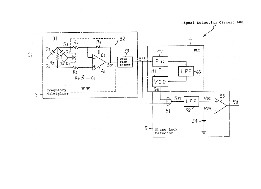
The signal detecting circuit 600 consists of a
frequency multiplier 3, a PLL 4 and a phase-lock detector 5
as shown in Fig. 4. In Fig. 4, frequency multiplier 3, PLL
4 and phase-lock. detector S are provided as frequency
multiplier 100, PLL 200 and phase-lock detector 300 in Fig.
3 respectively. The frequency multiplier 3 is provided so
as to operate under a condition that N = 2 in this
embodiment, so that frequency multiplier 3 consists of a
diode bridge 31 including four diodes D1, D2, D3 and D4 and
additional circuits such as: an LPF 32 consisting of an
operational amplifier A1, resistors R2, R3, R4 and R5 and
capacitors C1 and C2; and a waveform shaper 33. The diode
bridge 31 produces an output signal S31 specified in a
doubled frequency of frequency fi of input signal Si by
performing ~ullwave rectification to input signal Si. The
LPF 32 produces an output signal S32 by extracting a base
frequency component being a doubled frequency component of
input signal frequency Ei. The waveform shaper 33 produces
output signal S33 formed to a pulse-shaped wave by shaping
~ Ja~e~orrr7 5h~er ~3
signal S32. Therefore, ~ 33 produces
output signal S33 formed to a rectangle~shaped wave
specified in a doubled frequency of frequency fi of input
signal Si.
The PLL 4 consists of VCO ~1, PC ~'2 and LPF 43 each
having the same ~unction as VCO 11, PC 12 and LPF 13 in PLL
1 in Fig. 1 respec~ively. That is, the VCO 11 has a
- 13 -
~/ f' "~
free-running frequency f40 equal or nearly equal to a
doubled frequency f33 of a designated signal (metering
signal) included in input signal Sl. As a result, when
signal S33 from frequency multiplier 3 includes a signal
speeified in the doubled frequency f33, PLL 4 performs the
phase-lock between the doubled frequency f33 and a
oseillation frequency of VCO 41 and produees output signal
S41 having a phase different from a phase of the designated
signal as much as ~. A phase loek deteetor 5 in Fig. 4
qr
consists of an executive OR gate 51, ~ LPF 52, voltage
eomparator 53 and a referenee voltage souree 54 and deteets
that PLL 4 is in the phase-loek state with the designated
signal in signal S33, same as phase lock deteetor 2 in Fig.
1.
The above operation of signal deteeting eircuit 600
will be further explained in reference to Figs. 5a to 5h.
Fig. 5a shows a waveform of input signal Si. However, in
Fig. 5a, only a designated signal such as a metering signal
is depicted in a style of burst signal appearing in a time
interval between tl~ and tl3, omitting other signals such
as a voiee signal for simplicity. When the designated
signal is given to diode bridge circuit 31 as shown in Fig.
5a, diode bridge circuit 31 performs full-wave
rectifica-tion, producing signal S31 as shown in Fig~ 5b.
The LPF 32 extracts a doubled frequency component ol the
designated signal so as to produce siqnal S32 as shown in
- 14 -
,
'
-
.
~ J~
Fig. 5c. Then waveform shaper 33 shapes signal 532 so as
to produce signal S33 having squared-shaped wave as shown
in Fig. 5d. Since no signal is given to PLL 4 till tll as
shown in Fig. 5d, VCO 41 oscillates signal S41 specified in
a free-running frequency f0 in 50~ duty ratio till tll as
shown in Fig. Se. In such state, exclusive OR gate 51
outputs signal S51 in 50% duty ratio till t11 as shown in
Fig. 5f, and output voltage V52 from LPF 52 is maintained a
voltage lower than reference voltage V54 as shown in Fig.
5g, so that voltage comparator 53 produces detection signal
Sd representing an undetected state (logic "0~) as shown in
Fig. 5d.
When t11 passes, the phase of the signal S41 specified
in the free-running frequency f0 varies so as to lock to
the phase of signal S33 in PLL 4, taking a transit time
(from t11 to t12) as seen from comparison between Figs. 5e
and 5f in an interval from t11 to tl2. That is, during the
transit time, PLL 4 compares phase ~33 of signal S33 with
phase ~41 of signal S41 and varies the phase ~33 so that
the phase difference (~33 ~ ~41) becomes ~ by making phase
~33 follow phase ~41
In phase lock detector 5, as the phase difference (~33
~ ~41) closes to ~, the duty ratio of signal S51 from
exclusive OR gate 51 increases gradually and therefore
output voltage V52 -from LPF 52 increases. When the phase
difference becomes ~, the duty ratio of signal S51 reaches
~ rs ) ~
100% as shown in Fig. 5f and output voltage V52 exceeds
reference voltage V54 at tl2 as shown in Fig. 5g, so that
voltage comparator 53 produces detection signal Sd
presenting the detected state (logic "1") and the detected
state continues as far as V52 exceeds reference voltage V52
as shown in Fig. 5h.
When the burst input signal Si is over at tl3, TLL 4
is brought back to the free-running state at tl4 in a
opposite process to the above phase-lock process through a
transition time from tl3 to tl4 as shown after tl3 in Figs.
5f, 5g and 5h.
As seen from the above explanation of the embodiment,
since frequency multiplier 3 doubles the frequency fi f
input signal Si and the phase-lock is performed by using
the oscillation signal specified in the doubled frequency
in PLL 4, the transit time (from tll to tl2) for
establishing the phase-lock state on PLL 4 and the transit
time (from tl3 to tl4) for bringing PLL 4 back to the
free-running state can be shortened as less as one half of
those in the related art. As a result, the signal
detection can be performed, leaving a sufficient margin
though the signal to be detected is given to the signal
detecting circuit 600 in a short time.
In the above explanation of the e~bodimen-t, the
detection of the rnetering signal ir, t',e ~elephone s~stem
has been discussed. However, the present invention is not
- 16 -
~J ~ ~J ~J ~J tJ ~j
limited to apply the telephone system. The present
invention can be applied to other communication system or
signal processing system. The block diagram shown in Fig.
4 is nothing but an embodlment of the present invention.
Other circuits can be considered to achieve the object of
the present invention. In the explanation of the
embodiment in reference to Fig. 4 and Figs. 5a to 5h, the
multiplying factor N is set to two in frequency multiplier
3, however, other numeral larger than two is applicable to
N. The constitution of frequency multiplier 100, PLL 200
and phase lock detector 300 in Fig. 3 is concretely shown
in frequency multiplier 3, PLL 4 and phase lock detector 5
in Fig. 4 respectively, however, the constitution in Fig. 3
is not limited to that in Fig. 4.
~7ha-t -i-s-~-la-im~d ic.
.