Note: Descriptions are shown in the official language in which they were submitted.
2038587
A Controller For Distributing Loads
Amonq Call Processors
Background of the Invention
Field of the Invention
This invention pertains to a broadband ~exchange
and more particularly to a controller for distributing
loads among a plurality of call processors for
controlling a switching network used in a broadband
exchange per an asynchronous transmission mode.
Description of the Related Art
With the widespread use of data communication,
public switched networks are now required to provide
high-quality data communication, as well as the
traditional voice communication.
Broadband I S DN ( B - I S DN ) has begun to be utilized
for ~ communication networks not only for low-speed
data, such as voice data, but also for high-speed
data, such as moving images, and various interfaces
have been standardized. Unlike the traditional
switching method, a B-ISDN utilizing an asynchronous
transmission mode (ATM) can commonly carry at
different speeds various sorts of information, e.g.
voice data, moving image data and even continuous
information mixed with bursty information.
2038S87
An ATM communication network transmits and
exchanges information of different bands divided and
housed in fixed-length data units called cells,
instead of in variable-length packets as in
traditional packet communication. Cells containing
channel data and packet data are indiscriminately
multiplexed, transmitted over optical fibers at high
speed, and rapidly exchanged by hardware switches.
Thus, an ATM communication network can offer flexible
service requiring different transmission speeds and
makes efficient uses of transmission paths.
As described above, user information is divided
into several pieces according to its length and cells
are configured by adding headers, e.g. of a few bytes,
15to respective data, e.g. of 32 to 120 bytes,
comprising the divided pieces of information. A
header contains a virtual channel identifier (VCI) for
identifying the originating user of the corresponding
data. Thus, user information stored in cells is
multiplexed over ATM highways and transmitted and
exchanged to a destined terminal.
inp~ cell
-~An exchanger adds to inputtcd cclls information
as to how they should be exchanged in the exchange
system, so that they are autonomously transmitted over
a transmission path in the exchange network with their
2038587
3 28151-34
added header lnformatlon read by respectlve swltches ln the
exchanger. Hence, thls swltchlng method ls called a self-routlng
method, and the group of swltches wlthln the exchanger ls called a
self-routlng part.
Flgure 1 shows an exemplary conflguratlon of a
multlstage self-routlng part (MSSR) belng a swltchlng part ln an
ATM exchanger. The MSSR comprlses plural [generally three (3)]
stages of self-routlng modules (SRMs) each comprlslng a plurallty
of lnput and output termlnals. An ATM exchanger ls equlpped wlth
two such MSSRs, as shown ln Flgure 1, for both dlrectlons of data
transmlsslon.
Flgure 2 shows an exemplary conflguratlon of an SRM
shown ln Flgure 1. An SRM has pluralltles of lnput and output
llnes, and a crosslng polnt of an lnput llne and an output llne ls
provlded wlth a buffer. In Flgure 2, the SRM has four (4) lnput
llnes, four (4) output llnes and slxteen (16) buffers at
respectlve crosslng polnts.
As descrlbed earllerl at the entrance of an MSSR, the
respectlve lnput cells have added to themselves lnformatlon,
called tag lnformatlon, as to whlch lnput llne they are lnput to
and whlch output llne they are output from. Thus, tag lnformatlon
routes cells ln an MSSR. For lnstance, when SRMs are connected ln
three (3) sta~es as shown ln Flgure 1 and respectlve !SRMs have
four (4) output llnes as shown ln Flgure 2, respectlve lnput cells
have added to themselves 6-blt tags comprlslng three (3) sets of
2-blt tags speclfylng whlch of the four (4) output lines is
selected for outputtlng correspondlng to the three (3) SRM stages.
Meanwhile, as descrlbed earller, the header of each
2038~87
4 28151-34
input cell has added to ltself a VCI for ldentlfylng the
originating user of the cell. Thls VCI ls defined for respectlve
logical llnks among exchangers. Therefore, the header of an lnput
cell from an orlginatlng user has added to ltself the VCI
speclfylng the llnk wlth the exchanger of the precedlng stage,
over whlch llnk the cell ls transrnltted. The respectlve
exchangers replace the VCI added to the header of an lnput cell
with the new VCI speclfylng the llnk wlth the exchanger of the
succeedlng stage, over whlch llnk the cell ls transmltted. Thus,
cells are sequentlally transmltted to a plurallty of exchangers
towards a destlned termlnal.
A part called a Vlrtual Channel Converter (VCC) ln the
MSSR of an exchanger performs the above two processes, l.e.
replaclng VCIs and addlng tag lnformatlon, for the lnput cells.
The new VCI for replaclng the old VCI attached to an lnput cell
and the new tag lnformatlon for replaclng the old tag lnformatlon
are unlquely determlned by the old VCI. Accordlngly, a VCC ls
provlded wlth a converslon table enabllng lt to obtaln, from the
old VCI of an input cell, the new VCI to be added to the input
cell when it is output and the tag information.
When a user orlglnates a call, a call processor
determlnes, based on the trafflc condltlon ln the entlre ATM
network, the content of a VCC converslon table for obtalnlng, from
the old VCI, the approprlate tag lnformation and the new VCI,
which speclfy the optlmal transmlsslon path for the cells of the
origlnated call. Hence, the larger the MSSR and the more SRM
stages it contalns, the more complex the processes the call
processor must perform.
. ~
2û38587
28151-34
As such, lf one call processor performs all the
processes for all lncoming calls, which is ordinarily considered
for all processlngs, the network's response degrades.
An ordlnary solutlon to such a problem ls to dlstrlbute
load among a plurallty of call processors. However, there has
been no known load dlstrlbution
038587
-- 6 --
controlling method for effectively controlling MSSRs
comprising plural stages of SRMs. When an MSSR
comprises three (3) SRM stages, for instance, three
(3) processors may share the switching control in
respective stages. However, since the switch loads
in respective stages are not uniform, a crucial
problem still remains as to how efficiently a
switching can be performed by distributing loads
equally among all call processors.
Summary of the Invention
This invention is conceived based on the above
background and aims at controlling the switching
network of an ATM exchanger by uniformly distributing
loads among a plurality of call processors.
It is premised on a device for controlling the
load distribution among a plurality of call
processors by controlling the switch network in an ATM
broadband exchanger.
The first principle of this invention utilizes a
first call processing assignor and a switching state
controller, which are discussed below, and a call
processor to which is assigned a call processing by
the first call processing assignor, which performs
call processings according to the control state of the
switching state controller.
2038587
That is, the first call processing assignor
assigns the call processing for an originated call to
a plurality of call processors in the sequence of call
originations. The switching state controller
controls the respective usage of a plurality of
or cornpriS ing
-~ buffers composing~a switching network.
The second principle of this invention utilizes a
call processing assignment table memory and a second
call processing assignor, discussed below, as well as
a switching state controller similar to that utilized
in the first principle of this invention, and the call
processor to which is assigned a call processing by
the second call processing assignor, which performs
call processings according to the control state of the
15 switching state controller.
That is, the call processing assignment table
memory memorizes a table specifying which call
processor performs the call processing corresponding
to the channel identifier to be attached to the cells
20 in an originated call. The second call processing
assignor assigns the call processing for the
originated call to one of a plurality of call
processors by referring to the call processing
assignment table memory with the channel identifiers
25 corresponding to the originated calls.
2038587
8 28151-34
The second princlple can be varled to further lnvolve an
updater for updatlng the content of the call processing asslgnment
table memory accordlng to the control state of the swltchlng state
controller.
To summarlze, the flrst and second prlnclples of thls
lnventlon enable efflclent load dlstributlons by asslgnlng call
processlngs to a plurallty of call processors for controlllng the
swltchlng network of an ATM swltcher respectlvely ln the sequence
of call orlglnatlons and by the channel identlflers attached to
the respectlve cells of the orlglnated calls.
Accordlng to a broad aspect of the lnventlon there ls
provlded a controller apparatus for dlstrlbutlng loads among call
processors by controlllng load dlstrlbutlons among the call
processors and controlllng swltchlng network havlng a plurallty of
buffers for swltchlng call processlngs ln an asynchronous
transmlsslon mode broadband exchanger, sald controller apparatus
comprlslng:
flrst call processlng asslgnlng means for asslgnlng
orlglnated call processlngs to sald call processors ln an
orlglnated-call sequence; and
swltchlng state controlllng means, operatlng ln a control
state, for controlllng respectlve usages of the plurallty of
buffers comprlslng sald swltchlng network for swltchlng sald
orlglnated all processlngs,
whereln sald call processors to whlch the orlglnated call
processlngs are asslgned by sald flrst call processlng slgnlng
means perform call processlngs responslve to the control state of
sald swltchlng state controlllng means.
2038~
8a 28151-34
According to another broad aspect of the lnventlon there
ls provlded a controller apparatus for dlstrlbutlng loads among
call processors by controlllng load dlstrlbutlons among the call
processors ln controlllng a switchlng network comprised of buffers
for switching call processings in an asynchronous transmission
mode broadband exchanger, said controller apparatus comprising:
call processing assignment table memory means for storing a
table showlng whlch of the call processors control a processlng of
an orlglnated call havlng cells correspondlng to a channel
0 identifier attached to the cells of the originated call;
call processlng assigning means for assignlng originated-
call processings to one of said call processors by referring to
said call processing assigning table memory means with the channel
identifier corresponding to the originated call; and
switching state controlling means, operating in a control
state, for controlling respective usages of said buffers
comprising said switching network for switching said originated
call processings,
whereln the call processors to whlch the orlglnated call
processlngs are asslgned by sald call processlng asslgnlng means
perform sald orlglnated call processlngs responsive to the control
state of said switching state controlling means.
Brief Descrlpt lon of the Drawlnqs
Those in the same field can easily understand additional
purposes and features of this invention from the descriptions of
the principles and the preferred embodiments of this inventlon
together wlth the attached drawlngs. In the drawlngs,
Flgure 1 shows an exemplary conflguratlon of a
2038587
-
8b 28151-34
multistage self-routing part in an AT~ exchanger;
Figure 2 shows an exemplary configuration of a self-
routing module;
Flgure 3A is a block diagram illustrating the first
principle of this invention;
Figure 3B is a block diagram illustrating the second
principle of this invention;
2038~7
Figure 4 is a block diagram illustrating the
schematic configuration of an exemplary ATM exchanger
embodying this invention;
Figure 5 is a block diagram illustrating the
configuration of an exemplary self-routing module
embodying this invention;
Figure 6 is a block diagram illustrating the
configuration of an exemplary VCI converter (VCC)
embodying this invention;
Figure 7 shows an embodiment of a switching state
control table (SST);
Figure 8 shows exemplary data, for assigning call
processing according to the first principle of this
invention, stored in a memory (not shown) of an main
processor (MPR);
Figure 9 is a flowchart of a call processing
assignment operation executed by an MPR according to
the first principle of this invention;
Figure 10 is a flowchart of a call connection
processing operation executed by a call processor
(CPR);
Figure 11 is a flowchart of a bandwidth control
processing operation executed by an MPR;
Figure 12 shows an embodiment of a call
processing assignment table provided in a memory of an
2`'338587
28151-34
MPR accordlng to the second princlple of thls lnventlon; and
Flgure 13 ls a flowchart of a call processlng asslgnment
operatlon executed by an MPR accordlng to the second prlnclple of
this lnvention.
Descrlptlon of the Preferred Embodlments
Before descrlblng the preferred embodlments of thls
lnventlon, lts prlnclples are explalned by referrlng to Flgures 3A
and 3B. Thls lnventlon pertalns to a method for controlllng load
dlstrlbutlon among a plurallty of call processors (CPRs) 2-l
through 2-N, and for controlllng a swltchlng network l, provlded
ln an asynchronous transmlsslon mode (ATM) exchanger.
Flgure 3A ls block dlagram lllustratlng the flrst
prlnclple of thls lnventlon. In Flgure 3A, a maln processor (MPR)
3 sequentlally asslgns call processlngs for call-ups to CPRs 2-l
through 2-N ln the call-up orlglnatlon sequence. A swltchlng
state controller 4 collects usage lnformatlon about a plurallty of
buffers composlng or comprlslng the swltchlng network l ln the ATM
exchanger.
Flgure 3B ls a block dlagram lllustratlng the second
prlnclple of thls lnventlon. As shown, a call processlng
asslgnment table memory 5 ls
2~038587
provided, e.g. in a memory of the MPR 3, for
memorizing which CPR performs the call processing
corresponding to respective channel identifiers
attached to the cells in an originated call. The
switching state controller 4 shown in Figure 3B
operates similarly to that shown in Figure 3A. By
referring to the call processing assignment table
memory 5 with the channel identifier corresponding to
an originated call, the MPR 3 assigns a call
processing for the originated call to one of the CPRs
2-1 through 2-N. Further, for uniformly
distributing loads among CPRs 2-1 through 2-N, the MPR
3 periodically updates the contents of the call
processing assignment table 5 based on the information
stored in the switching state controller 4.
According to either the first or second principle
of this invention, the MPR 3 integrally controls the
assignment of call processings to CPRs 2-1 through 2-N
for controlling the switching network 1 in the ATM
exchanger either in the call-up origination sequence
or by the channel identifiers attached to the cells,
so that loads are distributed uniformly among CPRs 2-1
through 2-N, which route cells of the originated call
based on the information stored in the switching state
Controller.
2038587
Description of the Preferred Embodiments
~r~
The preferred embodiments of this invention ~;
explained in more detail, below. Figure 4 is a
block diagram illustrating the schema.tic configuration
of an exemplary ATM exchanger embodying this
nventlon .
In Figure 4, a VCI converter (VCC) 6 replaces the
virtual channel identifier (VCI) in an ATM cell
corresponding to the link with the exchanger in the
preceding stage, with the VCI corresponding to the
link with the exchanger in the succeeding stage, and
adds to the ATM cell a tag giving routing information
in a multistage self-routing part (MSSR) 7 comprising
plural stages of self-routing modules (SRMs ) .
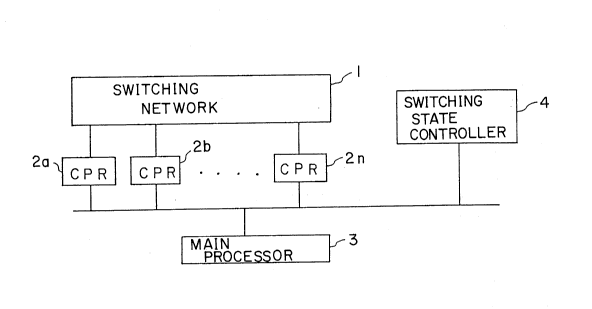
Three call processors (CPRS j 2a, 2b and 2c, as
well as a signaling device (SIG) for detecting a call
origination, are connected to a common bus 8 and
controlled by the main processor (MPR) 3.
Figure 5 is a block diagram illustrating the
configuration of an exemplary self-routing module
embodying this invention.
In Figure 5, self-routing modules (SRMS),
composing the MSSR 7 shown in Figure 4, comprise four
(4) buffers at 2*2 crossing points C0O through C11,
where ATM cells are exchanged by switching ATM cells
2038587
13 28151-34
input from lnput highways IHW #0 and #1 to output hlghways OHW #0
and #1.
Figure 6 ls a block diagram lllustrating the
conflguratlon of an embodlment of the VCI converter (VCC) 6 shown
in Flgure 4. The VCC 6 comprlses VCNVs (VCC driver) 10-0 through
10-3 for converting VCI and attaching tag information to the cells
input from input highways IHWO through IHW3 accordlng to an
lnstructlon from CPR2 and a VCCC (VCC channeler) 11 for
lnterfaclng between respective VCNVs 10-0 through 10-3 and
respectlve CPRs 2-1, 2-2 and 2-3.
The MPR 3 shown ln Flgure 4 ls provlded wlth a bandwldth
controller (BWC) whlch corresponds to the swltchlng state
controller 4 shown ln Flgures 3A and 3B. An orlglnatlng termlnal
maklng a call connectlon request notlfles the exchanger of the
lnformatlon on the bandwldth occupled by the call together wlth
the lnformatlon on the destlnatlon termlnal. The BWC controls the
swltchlng state by tracklng the informatlon on the bandwldth
occupatlon, e.g. values such as 64Kbps for a volce transmlsslon
and 50Mbps for a movlng lmage transmlsslon, from the orlglnatlng
termlnal and lnformatlon on the path over whlch the cells of the
call are routed ln the MSSR 7 when the
- 2038587
- 14 -
call is actually connected, instead of by monitoring
the actual usage of the buffers in the switching
network. Through such software processing
controls, the BWC easily realizes the switching state.
Figure 7 shows an embodiment of a switching state
control table (SST) retained in the above described
band information controller (BWC). The SST is
retained in a memory (not shown in the drawings) and
contains the sums of the bandwidths of the calls
currently being switched for the twenty-four (24)
1 0
combinations of Sxy (in the respective SRMs S0O, So1,
S02, S10, S11 and S12 each comprising 2*2 buffers) and
CLM (at the respective crossing points C0O, Co1, C10
and C11) and the maximum value MAX of the back widths
switchable at a particular crossing point (of an input
line and an output line in an SRM). In the example
of this embodiment shown in Figure 7, the MAX is set
to 150Mbps and 75Mbps bandwidth is currently being
used for switching calls at crossing point C0O in SRM
S0O. Since the MAX is greater than the sum of the
bandwidths of the calls currently being switched at
crossing point C0O in SRMoo, additional calls having
total bandwidths of 75Mbps can be switched at this
particular crossing point.
Whereas the basic configuration of this invention
2038587
- 15 -
is described as above, call processing assignments are
embodied according to the first or second principle of
this invention described earlier.
The embodiment of call processing assignments
according to the first principle are now explained in
detail.
Figure 8 shows exemplary data, for call
processing assignments according to the first
principle, stored in a memory tnot shown) of MPR 3.
The exemplary data comprise two data MAXCPF and CPF,
where MAXCPF indicates the total number of CPRs in an
exchanger and CPF indicates the number of CPRs in the
exchanger to which the next call processing is
assigned. Accordingly, the MAXCPF is constant
unless the configuration of the exchanger is changed.
Since there are three (3) CPRs 2a, 2b and 2c in the
schematic configuration shown in Figure 4, MAXCPF is
set to 3 here. CPF, the call processing assignment
flag, currently indicates #2 for 2b, but it changes
cyclically from #1 to #2 to #3 and then back to #1.
The call processing assignments and bandwidth
controls by the MPR3 according to the first principle
of the call processing assignments, as well as the
call connection processings by the CPRs 2a, 2b and 2c,
are explained in more detail. Here, the MPR 3
2038587
- 16 -
independently executes two processings (programs) of
call processing assignments and bandwidth controls,
and the CPRs 2a, 2b and 2c independently execute their
respectively assigned call connection processings.
Figure 9 is a flowchart of a call processing
assignment operation executed by the MPR 3 according
to the first principle of this invention. Described
below are the operations in the flow sequence
according to Figure 9.
STEP 91: A connection request is received from
1 0
the signaling device (SIG) 9. (Refer to Figure 4.)
STEP 92: The call processing assignment flag
(CPF) (Refer to Figure 8.) is read from a memory (not
shown).
STEP 93: The CPR corresponding to the number
indicated by the CPF (CPR 2a for CPF #1, CPR 2b for
CPF #2, and CPR 2c for CPF #3) is assigned with a call
processing and receives the information necessary for
the call processing, such as the VCI attached to the
npu,t
header of an inputtcd cell.
STEP 94: 1 is added to the CPF value, which is
stored in the memory as the new CPF.
STEP 95: The CPF is compared with the MAXCPF
and the processes are concluded when the CPF does not
exceed the MAXCPF.
2038S87
STEP 96: When the CPF exceeds the MAXCPF
(Refer to Figure 8.) read from the memory, the CPF
reverts to 1, which is stored in the memory.
Figure 10 is a flowchart of a call connection
processing operation executed by a call processor
(CPR) corresponding to the value of CPF. The
operation of the MPR3 assigns the call processing to
the CPR, based on the actions described in the
flowchart shown in Figure 9. Described below are
the operations in the flow sequence according to
1 0
Figure 10.
STEP 101: Based on the information (such as
p ~t
-~ the inputtcd VCI indlcating the link with the SRM in
the preceding stage, the input highway number and the
~stin~t;~
dc_tining terminal number) received from the MPR 3,
the new VCI indicating the link with the SRM in the
succeeding stage and the output highway number are
determined.
STEP 102: All possible route plans are
determined from among the input highway number and the
determined output highway number.
STEP 103: One of the route plans determined in
STEP 102 and the bandwidth of the call to be connected
are notified to the bandwidth controller (to be
described later).
2038587
STEP 104: If the MPR 3 judges that the route
plan can be instituted, the control moves on to STEP
105. Otherwise, it moves on to STEP 106.
STEP 105: The new VCI determined in STEP 101
and the tag information corresponding to the route
plan selected in STEP 103, together with the input VCI
corresponding to the calls to be connected, are
notified to the VCC 6. (Refer to Figures 4 and 5.)
STEP 10 6: The control reverts to STEP 103,
,
after the route plan~ selected in STEP 102 and judged
incapable of being instituted in STEP 1 04~ is
eliminated. If there is no route plan, the call
being processed is not connected and the calling
process is terminated.
Figure 11 is a flowchart of a bandwidth control
processing operation executed by the MPR 3. The MPR
3 notified of the bandwidth of a call and a route plan
according to the processing by a CPR in STEP 103 shown
in the flowchart of Figure 10 activates the bandwidth
controller for executing the processes shown in the
flowchart of Figure 11, and notifies the CPR of the
applicability of the route plan. Described below
are the operations in the sequence of the flow
according to Figure 11.
STEP 111: The MPR3 is notified of the route
20~8~87
- 19 -
plan of the MSSR 2 (Refer to Figure 4.) selected by
the CPR corresponding to a CPF, i.e. the transmission
path through the crossing points of the three stage
SRMs over which a cell in a call is transmitted, and
the size of the bandwidth occupied by the call.
STEP 112: The content of the switching state
control table (SST) is read. (Refer to Figure 7.)
STEP 113: The bandwidth value of the call
connected by the CPR corresponding to a CPF is added
to the used bandwidth value read from the SST
corresponding to respective crossing points on the
route plan obtained from the CPR corresponding to the
CPF.
STEP 1 1 4: It is judged whether or not
respective bandwidths in use obtained from the
addition performed in STEP 113 exceed the maximum
bandwidth MAX usable for switching read in STEP 112.
STEP 1 1 5: If there is no crossing point whose
usable bandwidth exceeds the MAX, the CPR
corresponding to the CPF is notified that the route
cannot be set.
STEP 1 16: The content of the SST shown in
Figure 7 is updated according to these usable
bandwidth values.
STEP 117: If there is any crossing point whose
2038587
~ o 281~1-34
usable bandwldth exceeds the MAX, the CPR correspondlng to the CPF
is notifled that the route cannot be set.
The above bandwldth controls and call processlng
asslgnments performed by the MPR 3 accordlng to the flrst
prlnclple of the call processlng asslgnments, as well as a
concrete example of the call connectlon processlng by a CPR ls
descrlbed below as procedures (l) through (16).
(1) The slgnalllng devlce (SIG) 9 notlfles the MPR 3, over the
common bus 8 shown ln Flgure 4, of a request to connect a call to
a deslred destinatlon termlnal number and the lnput VCI(=3). The
call ls assumed to be routed to lnput hlghway IHW #0 ln the MSSR
7.
(2) The MPR 3 actlvates the call processlng assignments shown ln
the flowchart of Flgure 9.
(3) The MPR 3 refers to a CPF stored ln a memory, not shown in
the drawlngs. (Refer to Flgure 8.) If the CPF value ls 3, the
MPR 3 notlfles CPR 2c correspondlng to the CPF, over the cornmon
bus 8, of the informatlon necessary for the call processlng, such
as the lnput VCI and the destlnatlon termlnal number.
(4) The MPR 3 termlnates lts call processlng asslgnments.
,
20385~7
(5) Based on the notification in procedure (3), the
CPR 2c corresponding to the CPF value 3 activates the
call connection processings shown in the flowchart of
Figure 10.
(6) The CPR 2c corresponding to the CPF value 3
determines the output VCI and the output highway
number OHW (#2, for instance), based on the
information notified in procedure (3).
(7) The CPR 2c corresponding to the CPF value 3
determines the possible route from IHW #0 to OHW #2.
(Refer to Figures 4 and 5.) In the above example,
the possible routes are as follows.
Route plan 1: S00, C00 ~ S01~ C01 ---~ S12~ Co1
Route plan 2: S00, C01 ---~ S11~ C01 --~~ S12' C10
(8) The CPR 2c corresponding to the CPF value 3
notifies the MPR 3 of route plan 1 and the bandwidth
(e.g. 100Mbps) of a call and waits for the reply on
the applicability of route plan 1.
(9) Upon being notified by the CPR 2c, the MPR 3
activates the bandwidth controller shown in Figure 11.
(10) The MPR 3 reads, from the switching state
control table (SST) shown in Figure 7, the respective
bandwidths used by the crossing points in route plan 1
notified in procedure (8).
(11) If, for instance, S00, C00 3 ' 01' 01
2038587
- 22 -
and S12, C01 = 10, are read from the SST as a result
of procedure (10), the MPR 3 adds to these values 100,
which is the bandwidth of the call to be connected.
(12) Since the bandwidth at no point exceeds the
MAX(=150) as a result of procedure (11), the MPR 3
judges that the present route plan is appropriate and
writes new values in the SST. That is, S0O, C0O =
' S01~ C01 = 145, and S12, C01 = 110.
(13) The MPR 3 notifies the CPR 2c corresponding to
the CPF value 3, over the common bus 8, of the
permission for a call connection.
(14) The MPR 3 terminates its bandwidth controls.
(15) Upon being notified of the permission for a
call connection, the CPR 2c corresponding to the CPF
value 3 notifies the VCC 6, over the SP bus 12 shown
in Figure 4, of the output VCI and the tag information
being route setting data, together with the input VCI
corresponding to the call to be connected. Thus,
the VCC 6 finalizes the content of the VCI conversion
table corresponding to the tag information and the
output VCI for an input VCI.
(16) The CPR 2c corresponding to the CPF value 3
terminates its call connection processings.
Embodiments of this invention according to the
second principle of the call processing assignments
2038~87
are explained in further detail. Figure 12 shows
an embodiment of a call processing assignment table
provided in a memory of an MPR according to the second
principle of this invention.
An embodiment according to the second principle
of the call processing assignments is equipped with a
call processing assignment table (ATBL), as shown in
Figure 12, in a memory (not shown) within the MPR 3,
instead of the data for call processing assignments
according to the first principle shown in Figure 8.
The call processing assignment table (ATBL) is
equivalent to the call processing assignment table
memory 5 according to the second principle of this
invention shown in Figure 3B and is provided inside
the MPR 3, together with the switching state
controller 4. The ATBL comprises values for the
input VCIs (hereafter called IVCIs), which are virtual
channel identifiers attached to the calls requesting
connections, and values for CNO, which are numbers of
the call processors ( CPRs ) assigned with the
processings of the calls corresponding to respective
IVCIs. In the example shown in Figure 12, there are
six (6) IVCIs 1 through 6. For instance, the
processings of connecting the call with its IVCI value
3 are assigned to the CPR with its CNO value 2. As
20385~7
- 24 -
described later, the the MPR 3 adjusts the loads for
the respective CPRs by updating the content of the
ATBL.
Now an embodiment of the call processing
assignments performed by the MPR 3 according to the
second principle is explained in more detail. The
bandwidth controls by the MPR 3 and the call
connecting processes by a CPR are essentially similar
to those processes based on the flowcharts shown in
` Figures 10 and 11, explained for the embodiment~
1 0
according to the first principle of the call
processing assignments.
Figure 13 is a flowchart of a call processing
assignment operation executed by an MPR according to
the second principle of this invention. Described
below are the operations in the sequence of the flow
according to Figure 13.
STEP 131: The MPR 3 receives connection request
from the signaling device (SIG) 9. (Refer to Figure
4.)
STEP 132: The MPR 3 determines the particular
CPR to which call processings are assigned by
referring to the ATBL shown in Figure 12 with the
input VCI (IVCI) of the call requesting a connection.
STEP 133: The MPR 3 receives information
2038~7
- 25 -
necessary for the call processing e.g. of the VCI
.~ i r p u~t
attached to the header of the inputtcd cell in
correspondence with the particular CPR determined in
STEP 132.
As shown in the above flow, according to the
second principle of the call processing assignments,
by using the ATBL such as that shown in Figure 12, the
MPR 3 performs a control to realize proper load
distributions among all pertinent CPRs. Here, the
10 MPR 3 adjusts the load for respective CPRs by updating
the content of the ATBL according to the traffic
condition in the network. For instance, the MPR 3
determines the content of ATBL according to the
content of the switching state control table (SST)
shown in Figure 7. Alternatively, the MPR 3
determines the content of the ATBL, so that frequently
used IVCIs are assigned to different to CPRs as much
as possible.