Note: Descriptions are shown in the official language in which they were submitted.
-1 - RCA 85,627
203878
ADJUSTABLE VIDEO/RASTER PHASING
FOR HORIZONTAL DEFLECTION SYSTEM
This invention relates to the field of horizontal deflection
circuits for televisions apparatus. More particularly, this invention
s relates to a system for providing a remotely adjustable phase
relationship between an incoming video signal and the synchronizing
signal used by the horizontal deflection circuit to assure horizontal
centering.
Television apparatus require that the circuits generating the
raster scan be synchronized with the video signal being displayed.
Standard NTSC video signals, for example, are displayed by
interlacing successive fields, each field being generated by a raster
scanning operation at a basic or standard horizontal scanning rate of
approximately 15,734 Hz.
The basic scanning rate for video signals is variously referred
to as fH, 1fH, or 1H. The actual frequency of a 1fH signal will vary
according to different video standards. In accordance with efforts
to improve the picture quality of television apparatus, systems have
been developed for displaying video signals progressively, in a
noninterlaced fashion. Progressive scanning requires that each
displayed frame must be scanned in the same time period allotted
for scanning one of the two fields of the interlaced format.
Accordingly, the horizontal scanning frequency must be twice that
of the interlaced video signals. The scanning rate for such
2s progressively scanned displays is variously referred to as 2fH or 2H.
A 2fH scanning frequency according to standards in the United
States, for example, is approximately 31,468 Hz. An unspecified
multiple rate may be referred to, for example, as nfH where n is an
integer greater than 1.
A problem that is encountered in sophisticated video
processing and deflection systems is the additional time which is
often necessary for the special signal processing of the video
information. The time delays resulting from the additional signal
processing can cause problems in synchronizing the deflection
circuit with the incoming video signal. Problems in properly
synchronizing the video/raster phasing can result in the picture
- 2 - RCA 85,627
20387~0
being uncentered horizontally. Typically, the video information is
received by the television apparatus one line at a time, at a first
horizontal scanning rate, for example 1fH. In a progressive scanning
system, for example, the video information may be stored, one or
more lines at a time, prior to being displayed. Sometimes, each line
is read out, or displayed, more than once. Sometimes, the
information in successive lines, or sets of lines, is processed, for
example, by being combined by interpolation. This can result in
additional lines of video information, which must be displayed along
o with the information in the original video signal. In a bidirectional
scanning system, for example, the video information for alternate
lines must be read out, or displayed, in reverse. In each case, the
nfH multiple rate synchronizing signals, 2fH for the example chosen,
must be delayed long enough to accommodate the signal processing.
It is desirable that circuits be standardized, which enables
some circuits to be shared by a number of different television
apparatus, which are otherwise provided with different signal
processing capabilities and systems. Some receivers can operate in
multiple modes, or process video signals from two or more
alternative sources, which may require more or less signal
processing time, and therefore require adjustable video/raster
phasing. Television apparatus, particularly those employing
sophisticated signal processing, have a substantial need for easily
controlling video/raster phasing, that is, the delay behNeen
synchronizing components in received video signals and scan
synchronizing signals generated for processed video signals. The
processed video signals are often displayed at faster scanning rates,
for example, requiring a video/raster phase adjustment for the delay
between a 1fH video signal in interlaced format and the 2fH scan
synchronizing signal required for a progressive horizontal scanning
deflection system.
It is an aspect of the invention to provide a means for easily
adjusting and maintaining the relative phase of synchronizing or
timing signals having different frequencies. A divider circuit may
be employed to generate a higher rate nfH timing signal, for example
2fH, from a clock signal. The divider circuit may be synchronized
- 3 - RCA 85,627
.~ 20387~3
with the timing signal, for example 1fH, generated by a first phase
locked loop to periodically reset the divider. Such a divider may be
embodied as a digital divider which can be preloaded with a digital
number, for example a four bit digital number, by digital control
5 signals. Such digital control signals may be transmitted over a
serial bus, as is found in many digitally controlled television
apparatus. A presettable or preloadable divider circuit can provide
coarse video/raster phasing in accordance with the preloaded digital
number to control centering of the picture. Changing the preloaded
10 number will move the second timing signal relative to the incoming
video signal in steps, for example two microsecond steps. A
presettable or preloadable divide-by-16 circuit operating from a
32fH clock, for example, can provide a 2fH timing signal.
It is another aspect of the invention to provide for
automatically controlled video/raster phase adjustment for
alternative video sources having inherently different timing
characteristics. Such alternative sources may include RGB inputs
and computer video driving circuits. Selection of an alternative
video source, for example by means of a remote control keypad, is
20 detected by remote receiver. The remote receiver is monitored by a
microprocessor which controls the television apparatus. The
microprocessor sends control data to a video source selector to
switch an alternative video source as the video output of the signal
processing circuitry. The microprocessor also transmits control
25 data to a video/raster phase adjustment circuit, to compensate for a
different timing characteristic of the alternative video source, to
assure that the picture will be properly centered.
It is still another aspect of the invention to provide manually
controlled fine phasing adjustment, for example in the range of zero
30 to two microseconds, in conjunction with the bus controlled phase
adjustment. In accordance with this aspect of the invention, the
fine phase adjustment may be implemented at a different point in
the successive chain of synchronizing and timing signals than the
point at which the bus controlled delay is implemented. The fine
35 phase adjustment may be inserted in the second phase locked loop,
rather than in the converter. The delay is made with respect to the
- 4 - RCA 8~,627
-
Z03~7~0
second timing signal, rather than with respect to the first timing
signal. In an illustrative embodiment, retrace pulses at the second
frequency are an input to a sawtooth signal circuit. The sawtooth
signal is one input to the phase comparator of the second phase
5 locked loop. The sawtooth circuit includes a ramp capacitor.
Varying the current used to charge the ramp capacitor in the
sawtooth signal circuit, for example by means of a manually
adjustable potentiometer, provides a fine phase adjustment.
Another problem that may be encountered in generating a
10 second horizontal synchronizing signal, for example at 2fH, from a
first horizontal synchronizing signal, for example at 1fH, in a video
signal, is assuring sufficiently precise symmetry, or constancy, of
the second synchronizing signal within the period of the first
synchronizing signal. The period of the second signal may vary due
to jitter caused by the first signal. If the symmetry of a 2fH
synchronizing signal, for example, is not very precise within any lfH
period, for example, the 2fH trace will be initiated at a different
instant every other line in the raster. This can cause a split raster
effect, as shown for example in FIGURE 5. A raster 2 has a first set
20 of alternate scan lines forming a picture portion R which diverges to
the right and a second set of alternate scan lines forming a picture
portion L which diverges to the left. Adjacent retrace pulses are of
different amplitude because different peak to peak yoke currents
flow during adjacent trace periods. Different peak to peak yoke
25 currents flow during adjacent trace periods because adjacent trace
periods are of different length. The amount of the scanning
difference between adjacent lines will depend on the magnitude of
the period difference and the overall energy recovery efficiency of
the deflection circuit. The effect of raster splitting is exaggerated
30 in FIGURE 5, wherein the scan lines of portion L begin sooner than
the scan lines of portion R. However, time differences between
adjacent trace periods on the order of only 100 nanoseconds may
cause unacceptable amounts of raster splitting.
An asymmetry in the first synchronizing signal, for example at
35 1fH, can be introduced by the very nature of the phase locked loops
used in the synchronizing circuits of horizontal deflection systems
- 5- RCA 85,627
20387~30
having two phase locked loops and forming part of a video speedup
system. The asymmetry might be inherent in some integrated
circuits as well. The absence of a retrace signal from which to
derive a feedback signal for the first phase locked loop, for example
s at the 1fH frequency, requires that the first timing signal be used as
a feedback signal to the phase comparator in the phase locked loop.
This can introduce a ripple at the frequency of the first timing
signal, resulting in the asymmetry of the first timing signal. The
asymmetry has been corrected in the past, for example, by special
10 signal processing circuits associated with operation of the first
phase locked loop and/or the circuit used for converting the first
timing signal to a second timing or synchronizing signal, at a
multiple frequency of the first timing signal. These can be costly,
and can result in unwanted delays in propagating synchronizing
15 information through the deflection circuitry.
In commonly owned and copending U.S. application 4g9,249,
filed 26 March 1990, a horizontal deflection system is described
having accurate synchronizing circuits for use in displaying video
signals at a multiple scanning rate, where an asymmetry stems from
20 a periodic perturbation of a synchronizing or timing signal. There, a
first phase locked loop generates a first timing signal at a first
horizontal synchronizing frequency corresponding to a horizontal
synchronizing component in a video signal. A converter circuit
derives from the first timing signal a second timing signal, having a
25 second frequency at a multiple of the first frequency and subject to
a variation in frequency at a rate corresponding to the first
frequency. A second phase locked loop receives the second timing
signal and a feedback signal in accordance with the second
frequency, and includes a voltage controlled oscillator for
30 generating a smooth horizontal synchronizing signal at the second
frequency. The second phase locked loop has a characteristic loop
response preventing the voltage controlled oscillator from changing
frequency as fast as the rate of variation of the second timing
signal. A horizontal output deflection stage may be coupled to the
35 second phase locked loop for synchronized horizontal scanning in
accordance with the second frequency. The two phase locked loops
- 6 - RCA 85,627
20;38780
are configured in tandem, in conjunction with the signal rate
converter, or multiplier. No additional signal processing circuitry is
needed to correct the symmetry of the timing signal generated by
the first phase locked loop or the symmetry of the multiple rate
5 timing signal derived by the converter.
It is yet another aspect of the invention taught herein to
provide for easily adjusting and maintaining a phase relationship
between received video signals and higher rate synchronizing or
timing signals generated by a horizontal deflection circuit which is
o compatible with the jitter control system described in U.S.
Application 499,249. The output of the divider, for example, may be
treated and processed as an uncorrected timing signal, whose
frequency variations will be averaged out by the second phase locked
loop, as described above.
In the Drawing:
FIGURE 1 is a block diagram of a horizontal deflection system
including synchronizing circuits for generating timing signals to
display 1fH video signals at a 2fH horizontal scanning rate, and
providing bus controlled phase adjustment and manually controlled
phase adjustment according to this invention;
FIGURE 2(a) is a block diagram illustrating the 1fH to 2fH
converter and bus controlled phase adjustment of FIGURE 1 in more
detai l;
FIGURE 2(b) is a block diagram illustrating an alternative bus
controlled phase adjustment, utilizing a digital phase shifter.
FIGURE 3 is a circuit diagram showing the second phase locked
loop of FIGURE 1 in more detail, including the manually controlled
phase adjustment;
FIGURES 4(a), 4(b), 4(c) and 4(d) are waveforms useful for
explaining the bus controlled phase adjustment and manually
controlled phase adjustment;
FIGURE 5 is a diagram illustrating raster splitting due to
asymmetry of the 2fH synchronizing signal within the period of the
1 fH synchronizing signal;
FIGURES 6(a), 6(b), 6(c), 6(d), 6(e) and 6(f) are waveforms
useful in explaining the raster splitting shown in FIGURE 5; and
- 7- RCA 85,627
2038780
FIGURE 7 iS a block diagram useful for explaining the
interaction of a microprocessor, alternative video sources and a bus
controlled video/raster phasing adjustment system.
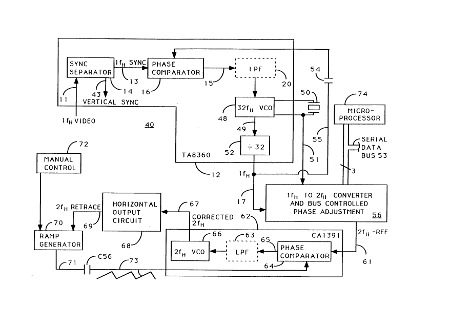
A horizontal deflection system for providing 2fH progressive
scanning of a 1fH video signal is shown in block diagram form in
FIGURE 1, and generally designated by reference numeral 40. A 1-
chip 12 may be utilized for constructing the a phase locked loop,
which generates a first timing signal as an output, at a nominal 1fH
rate. Industry type TA8360, for example, is 1-chip incorporating a
sync separator 14, a phase comparator 16 and a voltage controlled
oscillator 48. A 1fH video signal on line 11 is an input to sync
separator 14. The sync separator 14 provides vertical synchronizing
pulses on line 43 and 1fH horizontal synchronizing pulses on line 13.
The 1fH synchronizing signals on line 13, shown in FIGURE 6(a), are
an input to phase comparator 16. The output of phase comparator 16
on line 15, shown in FIGURE 6(b), is an error control signal input to
low pass filter 20. The frequency characteristic of the low pass
filter in the TA8360, for example, is determined primarily by
external timing components. Accordingly, block 20 is shown by
dashed lines. The external elements may be a series R-C network,
having a 10 microfarad capacitor and a 3K resistor coupled between
the capacitor and ground. Voltage controlled oscillator 48 operates
at a 32fH rate, responsive to a ceramic or L-C resonant circuit 50. A
nominal 32fH timing signal on line 49, shown in FIGURE 6(c), is an
input to a divide by 32 circuit 52. The output of the divide by 32
circuit on line 17 is a 1fH drive signal, shown in FIGURE 6(d). The
1fH signal is an input on line 55 to the other input of phase
comparator 16, which can result in the error control voltage of
FIGURE 6(b) being adversely modified by a 1fH ripple as shown. In
~o the event the width of the 1fH pulses being fed back to the phase
comparator 16 are too wide, the pulse width can be reduced, for
example by series coupled capacitor 54. The output of the resonant
circuit 50 at 32fH is also available externally of the 1-chip, on iine
51.
A 1fH to 2fH converter and bus controlled phase adjustment
circuit 56 is coupled to the 1fH output timing signal of the first
- 8 - RCA 85,627
20387~)
phase locked loop by iine 17 and to the resonant circuit 50 by line
51. Circuit 56 generates a timing signal designated 2fH-REF as an
output on line 61. The phase of the 2fH-REF signal relative to the
1fH timing signal on line 17 can be adjusted responsive to control
5 signals transmitted over serial data bus 53, for example by a
microprocessor 74.
Circuit 56 is shown in more detail in FIGURE 2(a). The 32fH
output of resonant circuit 50 on line 51 is an input to amplifier 90.
The output of amplifier 90 on line 91 is a CLOCK input to divide by
10 16 counter 58. Dividing a 32fH signal by 16 results in a 2fH signal.
Other multiples of a basic horizontal scanning frequency can be
produced by utilizing appropriate combinations of clock frequencies
and division factors. The 1fH timing signal on line 17 is an input to
edge detector 92. Edge detector 92 will detect the leading edges,
5 for example, of the pulses in the 1fH timing signal. The output of
the edge detector 92 on line 93 is the LOAD input to counter 58. The
divide by 16 counter 58 can be a 4-bit counter, having a 4-bit
parallel data bus 95 at its D or starting number input.
In accordance with another aspect of the invention, the use of
20 such counting means is compatible with the jitter control system
disclosed in commonly owned and copending U.S. application
499,249. A counting/dividing means, similar but without
presetting, is used in one embodiment thereof to generate a 2fH
timing signal from a 32fH clock signal. The 2fH signal is
25 synchronized with the horizontal synchronizing component of a video
signal by a 1fH timing signal synchronized with the synchronizing
component.
Remote control may be effected, for example, by means of the
serial data bus 53 (Fig. 1), of the kind which is often provided in
30 those television apparatus having a digital control architecture. A
serial data bus may comprise three lines as shown, generally
denoted DATA, CLOCK and ENABLE. A number from which to start
counting may be stored in shift register 94, by information supplied
over the serial data bus 53 by microprocessor 74. The data bus 53
3s can provide a starting number for the divide-by-16 counter 58 to use
at each occurrence of a pulse in the 1fH signal on line 17. The output
- 9 - RCA 85,627
2038780
Q of counter 58 is a 4-bit signal on parallel data bus 97. The 4-bit
signal is an input to decoding circuit 96, which supplies an output
pulse on line 99, for example at each occurrence of count 16. Each
starting number provides a different and corresponding number of
incremental, or coarse, phase adjustment delays. The signal on line
99 is an input to pulse width circuit 60, the output of which on line
61 is the 2fH-REF signal. Pulse width circuit 60 assures that the
width of the pulses in the uncorrected 2fH-REF timing signal on line
61 will be wide enough to assure proper operation of the phase
comparator in the second phase locked loop.
Alternatively, the adjustable delay may be implemented by a
digital phase shifter, as shown in FIGURE 2(b). The 1fH to 2fH
converter 56' is the same as in block 56 in FIGURE 2(a), except that
the counter 58 is not presettable and the shift register 94 is
omitted. The 2fH-REF signal on line 61 is an input to a digital phase
shifter 101. The amount of phase delay provided by the phase
shifter is determined by control signals transmitted over the data
bus 53 by the microprocessor. Line 51 also supplies the 32fH clock
signal to the digital phase shifter. If the digital phase shifter does
not have an input storage buffer adapted for receiving serial data, a
register similar to shift register 94 may be used for that purpose,
as in block 56 in FIGURE 2(a). The output of the phase shifter 101 is
a phase adjusted signal 2fH-REF', which for example becomes the
input to the second phase locked loop shown in block 62 of FIGURE 1.
The 2fH-REF signal is symmetrical only to the extent that the
initial duty cycle of the 1fH signal is fifty percent. The effect of
the 1fH ripple on the error control voltage for the 32fH VC0 is
reflected in the waveform of FIGURE 6(b). The error control voltage
periodically falls during each 1fH period. Accordingly, the output
frequency fvco f the 32fH VC0 falls periodically, during each 1fH
period. As the frequency falls, each subsequent output pulse from
the 32fH VC0 has a lower frequency. As the frequency decreases,
the pulse width 1/fvco increases. The divider circuit 58 doubles the
frequency of the 1fH signal, which has a period of 32 output pulses
of the 32fH VC0, by dividing the period in half, that is, into two
sixteen pulse periods. However, due to the periodically increasing
-1 0- RCA 85,627
2038781
pulse widths, the aggregate width of the first sixteen pulses, tA, is
less than the aggregate width of the next sixteen pulses, tB. When
the duration of tA is not equal to the duration of tB, the 2fH-REF
timing signal is not symmetrical within the period of the 1fH signal,
5 notwithstanding the precision of the digital divider. This
asymmetry can cause retrace pulses of alternating amplitudes Y1
and Y2 as shown in FIGURE 6(f), which can result in the raster
splitting. The 2fH-REF signal generated by the digital circuit must
therefore also be treated as an uncorrected signal, which requires
10 further processing.
The 2fH-REF signal is further processed by a second phase
locked loop 62. The second phase locked loop comprises phase
comparator 64, low pass filter 63 and a voltage controlled
oscillator 66. The phase locked loop 62 is embodied as an industry
type CA1391. The error output signal of phase comparator 64 on line
65 is a control input to voltage controlled oscillator 66, which
operates at a 2fH rate. The operating frequency of the oscillator and
the frequency response of the low pass filter in a type CA1391
oscillator are primarily determined by external timing components,
20 as shown in FIGURE 3. Accordingly, LPF 63 is shown by dashed lines.
The 2fH-REF is one input to phase comparator 64. The error
- control signal of phase comparator 64 on line 65 is an input to low
pass filter 63. The output of low pass filter 63 is a control input to
voltage controlled oscillator 66, which operates at a 2fH rate, and is
25 denoted 2fH VC0. The frequency characteristic of the low pass
filter 63 is determined by an external series R-C network formed,
for example, by 1.5 microfarad capacitor C53 and 2K resistor R68 as
shown in FIGURE 3. The output of voltage controlled oscillator 66 on
line 67 provides CORRECTED 2fH synchronizing signals for a
30 horizontal output circuit 68. The output of the horizontal output
circuit 68 on line 69 provides a 2fH signal in the form of 2fH
RETRACE pulses. The 2fH RETRACE pulses are an input to ramp
generator 70, which is subject to a manual phase delay by manual
delay circuit 72. The output of ramp generator 70 on iine 71 is AC
35 coupled by capacitor C56 to the other input of phase comparator 64
by line 73.
-1 1- RCA 8~,627
2038780
A circuit schematic for a portion of the block diagram shown
in FIGURE 1 is shown in FIGURE 3. The phase locked loop 62, as a
type CA1391 circuit, includes an oscillator 66, phase detector 64,
predriver 84, phase detector output driver 86 and Vcc voltage
5 regulator 87. The oscillator 66 is an RC type with terminal 7 used
to control frequency. An external capacitor C51 is connected from
terminal 7 to ground and charges through external resistance R62
coupled between terminals 6 and 7. When the voltage at terminal 7
exceeds an internal potential bias, capacitor C51 is discharged
10 through an internal resistor. This conduction causes generation of a
drive pulse, which terminates when the capacitor is sufficiently
discharged. Negative-going synchronizing pulses at terminal 3 are
phase compared with the sawtooth waveform at terminal 4, which is
derived from horizontal flyback or retrace pulses. If there is no
5 phase difference between the synchronizing signal and the sawtooth
waveform, there is no net output current at terminal 5. When a
phase offset occurs, current flows either in or out of terminal 5 to
correct the frequency. The duty cycle, or mark space ratio, of the
predriver 84 may be adjusted by setting the potential at terminal 8.
20 In the circuit of FIGURE 3, this is determined by the voltage divider
formed by resistors R63 and R64. Potentiometer R37, coupled to
terminal 7 through resistor R72, may be used to manually adjust the
frequency of oscillator 66.
The ramp generating circuit 70 comprises transistor Q4,
25 resistor R55 and capacitor C50. The ramp signal generated across
capacitor C50 is AC coupled to terminal 4 through capacitor C56. A
transistor Q2 and potentiometer R20 form a manually operable delay
circuit 72, which varies the current charging the ramp capacitor
C50. Variation of the time needed to charge capacitor C50 provides
30 a variable delay of approximately from 0-2 microseconds in the
relative phase of the 2fH-REF pulses and the CORRECTED 2fH pulses.
The CORRECTED 2fH output of predriver 84 on line 67 is an
input to a push-pull driver circuit comprising transistors Q5 and Q6,
which provides a 2fH DRIVE output signal to the horizontal output
35 circuit.
-1 2- P~CA 85,627
20387~30
The waveforms of FIGURES 4(a), 4(b), 4(c) and 4(d) illustrate
the relative phase positions of the 1fH and 2fH timing signals and
synchronizing signals generated by operation of the circuit shown in
FIGURE 1, 2 and 3. FIGURE 4(a) illustrates the 1fH SYNC pulses
separated by sync separator 14 and provided to phase comparator 16
on line 13. FIGURE 4(b) shows the 1fH output of the divide by 32
circuit 52 on line 17. The first phase locked loop is responsible for
maintaining the relative phase of the leading edge, for example, of
the 1fH pulses at the midpoint, for example, of the 1fH SYNC pulses.
FIGURE 4(c) illustrates the 2fH-REF signal generated by pulse width
circuit 60 on line 61, which is one of the inputs to phase comparator
64 of the second phase locked loop 62. FIGURE 4(d) is the 2fH
RETRACE signal on line 69, which is an input to the ramp generator
70. The difference in phase between the 1fH SYNC pulses and the
2fH-REF pulses, and therefore the CORRECTED 2fH pulses, is
adjustable, for example in two microsecond steps as explained
above, by bus control presetting of divide by 16 counter 58. Fine
adjustment, for example from O to 2 microseconds, is provided by
manually operable delay circuit 72, which provides for setting the
phase difference between the 2fH RETRACE PULSES and the 2fH-REF
signal. The adjustment is indirect, as the manual control circuit
actually adjusts the delay between the 2fH RETRACE pulses and the
sawtooth signal which is the other input to phase comparator 64. It
will be appreciated that bus control with different time delay steps
can be implemented by using different clock frequencies and/or
different counters having different numbers of bits to provide
different resolution. The manual phase adjustment can be modified
to enable manual adjustment over a range corresponding to the
incremental time delay steps provided by bus control.
An example of adjusting the video/raster phase delay to
accommodate alternative video sources is shown in the block
diagram of FIGURE 7. The horizontal deflection circuit 80 depicted
in FIGURE 7 is similar to the circuit 40 shown in FIGURES 1-3,
except that alternative video sources and means for switching
between the alternative video sources is also illustrated. The
details of the 1-chip 12, the converter 56 and the second phase
-13- RCA 85,627
2038~80
locked loop 62 are omitted for clarity, but may be as shown in
FIGURES 1-3. Video source selector switches are features of some,
but not all 1-chips.
The microprocessor 74 is coupled to a remote control receiver
5 79 and to a video source selector 88, for example by the serial bus
53. The remote receiver 79 is coupled to a keypad, for example a
remote control keypad 89, by a radio or infrared transmission 85.
Video source A, illustrated in block 81 as a composite video signal,
is coupled to a separation and demodulation circuit 83. Video source
10 A may therefore represent a broadcast or cablecast composite video
signal, for example a 1fH interlaced video signal. The outputs of the
separation and demodulation circuit 83 are drive signals for the
video guns, designated A RED, A GREEN and A BLUE, and a
synchronizing signal, designated A SYNC. These outputs form one set
5 of inputs to the video source selector 88. The other set of inputs to
video source selector 88 are supplied by an alternate video source,
which is illustrated in block 82 as an RGB video source. An RGB
video source may be supplied, for example, by a computer. The
outputs of the alternative video source 82 are designated RGB RED,
20 RGB GREEN, RGB BLUE and RGB SYNC. It will be appreciated that a
different delay in videotraster phasing may be necessary to assure
proper centering of the picture. The video source selector 88 has
outputs designated RED OUT, GREEN OUT, BLUE OUT and SYNC OUT. It
is assumed, for purposes of illustration, that the timing signals of
25 the alternative video sources are sufficiently different that, in the
absence of a video/raster phase adjustment, the picture may not be
properly centered horizontally when selecting the alternate video
source.
Selection of an alternative video source, for example by means
30 of a remote control keypad 89, is detected by remote receiver 79,
and monitored by microprocessor 74. Microprocessor 74 sends
control data to the video source selector 88 to provide the video
drive signals and synchronizing signal form the alternative video
source instead of video source A. Microprocessor 74 also transmits
3s control data to the phase adjustment circuit in block 56, to
-1 4- RCA 85,627
Z038 ~80
compensate for the different timing of the alternative video source,
to assure that the picture will be horizontally centered.
In accordance with an aspect of the invention, an optimum
phase relationship can therefore be established between the
5 incoming video signal and the scan synchronizing signal utilized by
the horizontal deflection circuit to generate the raster. The
optimum phase relationship can be achieved by utilizing both the bus
controlled and manually controlled phase adjustment circuits for
coarse and fine phase adjustments, respectively. It will be
10 appreciated that coarse and fine are relative terms. The coarse
adjustment can be made sufficiently fine, for a particular purpose,
by decreasing the time delay of each incremental step. Whenever the
microprocessor is called upon to initiate a special video display
function or process, or to display an alternative video source,
5 requiring more or less phase delay between the video signal and the
scan synchronizing signal, the phase delay can be changed
accordingly by the microprocessor. This arrangement provides the
maximum flexibility for optimizing the video/raster phase delay for
all video processes and all video sources.