Note: Descriptions are shown in the official language in which they were submitted.
-1- 2039373
DIGITAL DATA COMMUNICATION SYS
BACKGROUND OF TIIE INVENTION
The present inYention relates to a digital data communication
system and, more particularly, to an adaptive channel impulse
response estimation system for estimating an impulse response
5 reliably at the receiving side of a channel which varies with time
and suffers from distortions due to intersymbol intereference and
an adaptive maximum likelihood sequence estimation (MLSE)
system for demodulating received data correctly by reduci~g the
influence of demodulation delay.
In digital communication over a channel which varies with
time and suffers from intersmbol interference as mentioned
above, the receiving side needs an adaptive equalizer adapting
itself to the characteristic of the channel to demodulate received
data correctly. If the impulse response of the channel is known,
15 the adaptive equalizer can be constructed to satisfy a
predetermined characteistic. It is therefore necessary to estimate
the impulse response of the time-varying channel from a received
signal, so that the equali2er may follow the channel. A
conventional implementation for estimating a channel impulse
2û response from a received signal consists in applying the output of
Z039373
a decision unit to a replica generating filter which generates a
replica of a receiYed signal and is implemented as a transversal
filter, comparing the replica with the actual received signal, and
controlling the tap coefficients of the filter in such a manner as to
5 reduce a difference therebetween, as disclosed in, for example,
Proa~is "Digital Communications", McGraw-Hill, lg83 (referred to
as PRIOR ART I hereinafter). In this kind of system, the tap
coefficients of the replica generating filter are outputted as an
estimated channel impulse response, and an adaptive equali2er is
10 controlled in matching relation to the estimated channel impulse
response. However, estimating a channel impulse response from
a decision result is disadvanageous in that a decision error would
cause the replica generating filter to diver~e and thereby render
the operation of the adaptive equalizer itself unstable, resulting in
15 error propagation.
To reduce decision errors, the adaptive equation system may
be implemented by MLSE using '~literbi algorithm, as taught in,
for example, Xayes "The ~iter~i Algorithm Applied to Digital Data
Transmission", IEEE, Communication Society, 19 7 5, No. 13
2 0 (hereinafter referred to as PRIOR ART II) . This scheme
successfully reduces decision errors and, therefore, stabilizes the
operation of the replica generating filter so long as t~e channel
varies slowly. However, when the channel variation is rapid, the
ability of the filter to follow the channel variation is degraded due
2 5 to demodulatiorl delay particular to the MLSE scheme with the
203~373
result that the decision error is aggravated.
Even linear equation or decision feedback equation cannot
eliminate the above-discussed problems since the estimated
channel impulse response achievable therewith is unstable.
SU~ Y OF THE IN~ENTION
It is therefore an object of the present invention to provide a
digital data communication system which allows the receiving side
to demodulate received data correctly even when the channel
10 varies with time and suffers from distortions due to intersymbol
interference.
It is another obiect o the present inYention to provide an
adaptive channel impulse response estimation system which allows
the receiving side to estimate a channel impulse response
15 reliability even when the channel varies with time and suffers
from distortions due to intersymbol interference.
It is another obiect of the present invention to provide an
adaptiYe MLSE system which allows the receiving side to
demodulate received data correctly and reliably even when the
20 channel varies with time rapidly and suffers from distortions
ascribable to intersymbol interference.
In accordance with the present invention, an MLSE system for
a digital data communication system which tra~smits data oYer a
transmission channel comprises a circuit for estimating an MLS on
2 ~ the basis of a receiYed signal and a predicted futu}e channel
~4~ 203~373
impulse response applied thereto, and outputting the result of
estimation, a circuit for generating a replica of the recei~7ed
signal on the basis of the result of estimation and internal states
thereof, producing a difference between the received signal and
5 the replica, changing the internal states in a direction for
reducing the difference, and outputting the result of change, and
a circuit for predicting a future channel impulse response on the
basis of the result of change applied thereto by using the result of
change as a past change in internal states, and outputting the
10 result of prediction.
Also, in accordance with the present invention, an adapti~e
MLSE apparatus using Viterbi algorithm and applicable to a digital
data communication system which transmits data over a
transmission channel comprises a matched filter to which a
15 recei~ed signal and a predicted future channel impulse response
are applied, a branchmetric compute circuit for calculating, in
response to the predicted future channel impulse response and an
output of the matched filter, a branchmetric of the recei~ed
sig~al and outputting the branchmetric, an add, compare and
2 0 select (ACS) circuit for estimating an MLS in response to . an
output of the branchmetric compute circuit, and outputting the
result of estimation, a delay circuit for delaying the recei~ed
signal by a demodulation time in which the result of estimation is
outputted, a recei~ed signal regenerating filter for regenerating
25 and outputting the receiYed signal in response to an output of the
~5~ 20~9373
ACS circuit, a filter control circuit for updating, in response to
an output of the delay circuit, an output of the received signal
regenerating filter, and internal states of the received signal
regenerating filter, the internal states of the received signal
5 regenerating filter such that a difference between the output of
the delay circuit and that of the received signal regenerating filter
decreases, and a channel impulse response predict circuit for
predicting, in response to an output of the received signal
regenerating filter control circuit and by using the output as a
10 past change in the internal states of the received signal
regenerating filter, a future path impulse response and outputting
the result of prediction as the predicted future channel impulse
response.
Further, in accordance with the present invention, an
15 adaptive channel impulse response estimation system for a digital
data communication system which transmits data over a
transmission channel comprises a first internal state output
circuit for generating, in response to a result of decision, a
received signal and an estimated channel impulse response, a
20 replica of the received signal and outputting first internal states,
a control pulse output circuit for detecting a decision error in
response to the first internal states and, when detected a decision
error, outputting a control pulse, a second internal state output
circuit for replacing, in response to the received signal and first
2 5 internal states, the first internal states with second internal
2039~73
--6--
states to control error propagation when the control pulse output
circuit has outputted the control pulse and outputting the seco~d
internal states, or outputting the first internal states as the
second internal states without replacement when the control pulse
5 output circuit does not output the control signal, and an
estimated value output circuit for updating the second internal
states to output the estimated channel impulse response.
BRIEF DESCRIPTION OF THE DRAWINGS
The above and other ob~ects, features and advantages of the
present invention will become more apparent from the following
detailed description taken with the accompanying drawings in
which:
Fig. 1 is a bloc~ diagram schematically showing an adapti~e
channel impulse response estimation system representatiYe of a
first embodiment of the present inYention;
Fig. 2 is a blocX diagram schematically showing a specific
construction of a replica generating filter included in the
embodiment;
2 0 Fig. 3 is a bloc~ diagram schematically showing an adaptiYe
channel impulse response estimation system representati~e of a
second embodiment of the present invention which is applied to an
MLSE system;
Fig. 4 is a block diagram schematically showing a specific
2 5 construction of a propagation error suppress circuit included in
_7_ 2039373
the second embodiment;
Fig. 5 is a schematic block diagram of an adaptive MLSE
system which is a third embodiment of the ~resent invention;
Fig. 6 is a schematic bloc~ diagram an adaptive MLSE system
5 representative of a fourth embodiment of the ~resent invention;
Fig. 7 is a block diagram schematically showing a specific
construction of a regenerating filter and a filter control circuit
included in the fourth embodiment; and
Fig. 8 is a block diagram showing a specific construction of
10 an impulse response predict circuit included in the construction of
Fig. 7.
/
2039373
DESCRIPTION OF THE PREFERRED EMBODIMENTS
Preferred embodiments of the digital data communication
system in accordance with the present invention will be described
with reference to the accompanying drawings.
First Embodiment
Referring to Fig. 1 of the drawings, a first embodiment
pertaining to the adaptiYe channel impulse response estimation
system will be described. As shown, the system has input
terminals 12 and 14, a replica generating filter 16 for generating
a replica of a received signal, an internal state convert circuit
18, a decision error detect circuit 2 0, an internal state update
circuit 22, and an output terminal 24. A signal representative
of the result of decision is applied Yia the input terminal 12 to
the replica generating filter 16. The received signal is applied
via the input terminal 14 to the replica generating filter 16 and
internal state convert circuit 18. As shown in Fig. 2, the filter
16 may be implemented as a 3-tap transYersal filter having an
input terminal 32 which is supplied with the signal of the result
of decision and an input terminal 34 which is supplied with the
received signal, shift registers 36, 38 and 40, tap coefficient
memories 42, 44 and 46, multipliers 48, 50 and 52, an adder
54, a subtractor 56, output terminals 58, 60, 62 and 64, and
input/output terminal 6 6, 6 8 and 7 0 . The tap coefficients of
the transYersal filter 16, i. e., the outputs appearing on the
input/output terminals 66, 68 and 70 are the estimated values
2039373
of channel impulse response. The tap coefficients, signals
stored in the registers 36, 38 and 40, i. e., outputs appearing
on the output terminals 60, 6Z and 64, and an error signal,
i. e., output appearing on the output terminal 58 define the
5 internal states of the filter 16.
In response to the input signal, the replica generating filter
16 outputs the current internal state thereof to the internal state
convert circuit and decision error detect circuit 2 0. The
decision error detect circuit 2 0 determines whether Or not a
10 decision error has occurred on the basis of the internal states.
On determining that a decision error has occurred, the detecting
circuit 20 feeds a start control pulse to the internal state convert
circuit 18. In response to the control pulse, the convert circuit
18 converts the internal states on the basis of the received signal
15 from the input terminal 14 and the internal states of the filter 16
in such a manner as to eliminate error propagation. The result
of conversion is applied to the internal state update circuit 2 " .
When the start control pulse is not applied from the detect circuit
20 to the convert circuit 18, the convert circuit 18 outputs the
2 0 internal states of the filter 16 without converting them. On
receiving the internal states, the update circuit 22 feeds updated
values of tap coefficients to the filter 16 while feeding the
estimated channel impulse response values, i. e., updated tap
coefficients to the output terminal 24.
-lO- 2039373
Second Embodiment
An alternative embodiment of the present invention is shown
in Fig. 3 and implemented by applying the adaptive channel
impulse response estimation system to the MLSE system. As
5 shown, the system has an input terminal 8 2, an MLSE circuit
84, a replica generating filter 86, an error propagation suppress
circuit 8 8, a comparator 9 0, a tap coefficient updatae circuit
92, and an output terminal 94. The replica ~enerating filter 86,
error propagation suppress circuit 8 8, comparator 9 0 and tap
10 coefficient update circuit 9 2 constitute the gist of this
embodiment. The filter 86 may also be implemented as a 3-tap
transversal filter, as shown in Fig. 2.
A receiYed signal arrived at the input terminal 82 is applied
to the MLSE circuit 8 4, replica generating filter 8 6, and error
15 propagation suppress circuit 8 8 . Generally, when the MLSE
circuit 84 involves demodulation delay, it is necessar~ to delay
the received sig~al by the demodulation delay before feeding it to
the filter 8 6 and suppress circuit 8 8 . In the following
description, let the demodulation delay in the MLSE circuit 84 be
2~ assumed to be zero. The MLSE circuit 84 executes MLSE with the
received signal and applies the result of estimation to the output
terminal g4 and filter 86. In response, the filter 86 produces a
signal representative of a difference between the received sig~al
come in through the input terminal 8 2 and a received signal
5 replica which the filter 8 6 generates. In this embodiment, the
-11- 203937:~
internal states (decision pattern) of the shift registers 3 6, 3 8
and 40 appearing on the output terminals 60, 62 and 64, Fig.
2, tap coefficients appearing on the input/output terminals 66,
68 and 70, Fig. 2, and the error signal appearing on the output
5 terminal 5 8, Fig. 2 are representative of the internal states of
the filter 86. The filter 86 deli~ers such an internal states to the
error propagation suppress circuit 8 8 and comparator 9 0 . The
comparator ~ 0 detects, among the input internal states, the
le~el of the error si~nal and compares it with a predetermined
1~ threshold level which exceeds, for example, a decision range If
the level of the error signal is higher than the threshold level,
the comparator 9 0 feeds a start control pulse to the error
propagation suppress circuit 8~ determinin~ that a decision error
has occurred. In response to the control pulse, the suppress
15 circuit 88 converts the internal states from the filter 36 in such a
manner as to suppress error propagation and then outputs the
result of con~ersion.
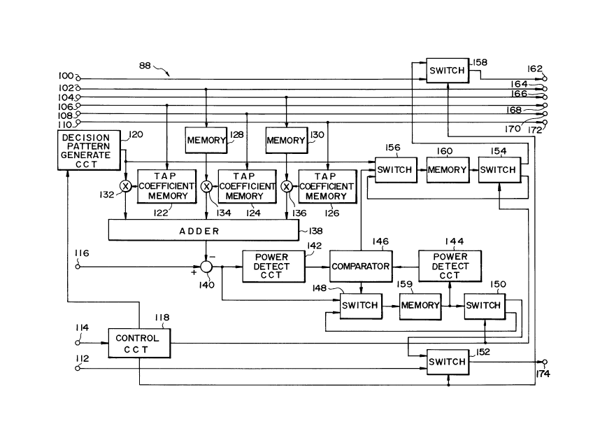
Fig. 4 shows a specific construction of the error ~ropagation
suppress circuit 88. The construction of Fig. 4 is applicable to
20 a case wherein the filter 86 has three taps as sho~vn in Fig. 2,
i. e., the number 7~ of shift registers is "3" while the number ~z of
signals in each shift register is "1". Generally, the construction
is extendible e~en when ~2 and m each has any other value. In
Fi~. ~, there are shown input terminals 100, 102, 104, 106,
lC8, 110, 112, 11 and 116, a control circuit 118, a decision
-12- 2039373
pattern generate circuit 120, tap coefficient memories 122, 124
and 126, memories 128 and 130 for storing signals of shift
registers, multipliers 132, 134 and 136, an adder 1~8, a
subtractor 140, power detect circuits 142 and 144, a
comparator 146, switches 148, 5û, 152, 154, 156 and 158,
memories 159 and 160, and output terminals 162, 164, 166,
168, 170, 1 /'2 and 1~'4.
The internal states from the filter 86 are applied to the input
terminals 100, 102, 104, 106, 108, 110 and 112. Specifically,
signals on the output terminals 60, 62 and 64, Fig. 2, are
respectively applied to the input terminals 10 ~, 102 and 104,
signals on the output terminals 66, 58 and 70, Fig. 2, are
respectiYely applied to the in~ut terminals 106, 108 and 110,
and the signal on the output terminal 58, Fig. 2, is applied to
the input terminal 112. Applied to the input terminals 114 and
116 are the control pulse from the comparator 90 and the
receiYed signal, respectively. On receiving the control pulse Yia
the input terminal 114, the control circuit 118 deliYers a start
control signal to the decision result pattern generate circuit 120.
The control circuit 118 feeds control signals to the switches 150
and 154 and thereby causes them to deliver input signals to,
res~ectively, the switches 148 and 156 as initial states. When
the decision pattern generate circuit 120 completes processing,
the control circuit 118 causes the switches 150 and 154 to deliYer
input signals to the switches 15 2 and 159, respectivelY.
-13- 20~9~73
Further, the control circuit 118 applies control signals to the
switches 152 and 159 to cause them to output the signals from
the switches 150 and 154, respectiYely. The switches 152 and
159 outputs respectively the signals from the input terminals 112
and 100 when not supplied with the control signals from the
control circuit 118.
In response to the control signal from the control circuit
118, the decision pattern generate circuit 120 generates all of
mT possible decislon patterns. In the embodiment, m is assumed
to be "1 ". The decision patterns are fed from the decision
pattern ~enerate section 120 to the multiplier 132. The internal
states of the filter 86 are stored in the memories 128 and 130.
The multipliers 132, 134 and 136 and adder 138 weight the
si~nals stored in the memories 128 and 130 and the signal from
the decision pattern generate circuit 120 by the signals stored in
the tap coefficients memories 122, 124 and 126 and then add the
weighted signals. The subtractor t 40 produces a signal
representati~e of a difference between the output of the adder
138 and the received signal come in through the input terminal
114. This output of the subtractor 140 is fed to the power
detect circuit 142 and switch 148. Initially, the switch 148 is so
set as to select the output of the subtractor 140 a~d apply it to
the memory 158. The memory 158 usually delivers the content
thereof to the switch 150 and power detect circuit 144.
The power detect circuit 1 ~14 detects the power of the input
-14- 2039373
signal and feeds it to the comparator 146. In response, the
comparator 146 selects smaller one of the outputs of the power
detecting circuits 142 and 144. The comparator 146 controls
the switch 148 such that if the output of the power detect circuit
144 is smaller than that of the power detect circuit 142, the
output of the switch 150 is fed to the memory 158 or, if
otherwise, the output of the subtrac~or 140 is fed to the memory
158. As a result, the memory 58 stores an error signal
mi~imi~ing the power at all times. At the same time, the
comparator 1~6 controls the switch 156 such that if the output
o~ the power detect circuit 142 is smaller than that of the power
detect circuit 1 ~4, the output of the decision pattern generate
circuit 120 is fed to the memory 160 or, if otherwise, the output
of the switch 154 is fed to the memory 60. Initially, the switch
156 is so set as to select the output of the decision patter
generate circuit 120. Then, the memory 160 always stores a
decision pattern which provides the minimum error signal power.
By the above procedure, when a control pulse is fed from the
comparator 146 to the control circuit 118, internal states
converted in such a manner as to suppress error propagation are
caused to appear on the output terminals 160, 162, 164, 166,
168, 170, 172 and 17~. When the control si~nal is not fed to
the control circuit 118, the input internal states are outputted
without being converted at all.
The internal states undergone conversion as stated above are
-15- 2039373
transferred to the tap coefficient update circuit 92. Assume that
the filter 86 and the error propagation suopress circuit 88 have
the specific constructions shown in Figs. 2 and 4, respectively.
Then, the tap coefficients of the filter 86 applied to the output
terminals 162, 164 and 166, Fig. ~, are the estimated values of
the path impulse response at a time K-l. The update circuit 92
determines tap coefficients at a time ~ by using the converted
internal states and algorithm such as LMS algorithm taught in
the ~reviously stated PRIOR ART I. Such tap coefficients are
ap~lied to the ~LSE circuit 84 and filter 86. The MLSE circuit 84
and filter 8 6 each continues adaptive oeprations while updating
the internal states thereof in response to the output of the update
C~ ~i
-16- 20~9373
Third Embodiment
Referring to Fig. 5, a third embodime~t of the present
invention pertaining to the adaptive MLSE system will be
described. As shown, the system has an input terminal 182, an
MLSE circuit 184, a received signal regenerating filter 18 6, a
channel impulse response predict circuit 188, and an output
terminal 190. A received si~nal is applied to the MLSE circuit
184 and received signal regenerating filter 186 via the input
terminal 182. The MLSE circui~ 184 executes MLSE with the
received si3nal and feeds the result of estimation to the outptut
1~ 0 and filter 18 6 . The filter 18 6 generates a replica of the
received signal on the basis of the result of estimation and the
internal states thereof. Further, the filter 18 6 compares the
received signal come in through the input terminal 18 2 and the
replica and updates the internal states thereof in such a manner
as to reduce their difference or error. The updated states of the
filter 186 are fed to the channel impulse response predict circuit
18 8 . In response, the predict circuit 18 8 predicts a future
channel impulse response and delivers the result of prediction to
the ~ILSE circ~lit 184. In response, the MLSE circuit 18~ changes
the internal states thereof in matchin~ relation to the future
chan~el impulse response.
Fourth Embodiment
Fig. 6 shows a fourth embodiment of the present invention
2 5 which is concerned with the adaptive MLSE system. In Fig. 6,
-17- 2039373
there are shown an input terminal 202, a matched filter 204, a
branchmetric compute circuit 206, an add, compare and select
(ACS) circuit 208, a delay circuit 210, a received signal
regenerating filter 212, a channel impulse response predict
S circuit 214, an output terminal 216, and a filter control circuit
218. The matched filter 2~2, banchmetric compute circuit 206
and ACS circuit 208 constitute in combination an MLSE circuit
using Viterbi algorithm. The matched filter 204 and
branchmetric compute circuit 206 each has dependency on channel
10 impulse response (see PRIO~ ART II). The received signal from
the input terminal 202 is applied to the ~LSE circuit constituted
by the matched filter 204, branchmetric compute circuit 206, and
ACS circuit 208, and to the delay circuit 210. The ACS circuit
208 delivers the ML,SE result to the regenerating filter 212. The
15 replica of the received signal and the internal states of the
regenerating filter 212 are applied to the filter control circuit
218. Also applied to the filter control circuit 218 is the received
signal haYing been delayed by an ~ILSE modulation time by the
delay circuit 210. Assuming that the channel impulse response
20 has a length of ~3 n~ then the filter 212 and filter control circuit
218 may be implemented as a transversal filter and a processor,
as shown in Fig. 7.
In Fig. 7, there are shown input terminals 222 and 224, shift
registers 226 and 228, multipliers 230, 232 and 234, an adder
236, a subtractor 238, a processor 240, circuits 242, 24d~ and
-18- 2039373
246 for generating channel impulse response values ho (k), hl (k)
and h2 (k), respectivelY, and output terminals 248, 250 and 252.
The estimated channel impulse response values 242, 244 and 246
and the contents of the shift registers 226 and 228 are the
5 internal states of the regeneratin~ filter 212. At a time k, the
result of decision a (k) from the ACS circuit 208 is applied to the
input terminal 222. The multipliers 230, 232 and 234 multiply
the results of decision a (k-2) to a (k) by the channel impulse
response values ha (k) to h2 (k) estimated at the time k, while the
10 adder 236 adds the resulted products. As a result, a replica of
the ~th received signal r ~k) appears on the output of the adder
236. On the other hand, a received signal r (k3 delayed by the
delay circuit 210 arrives at the input terminal 224. The
sllbtractor 238 produces a difference or error (h (k) ) between
15 the received signal r ~k) and the output of the adder 236 and
delivers it to a processor 240. By using an adaptation
algorithm, the processor 240 updates the channel impulse
response vaues h~ (k) to h2 ~k) such that the square mean, for
example, of the error ~ (h (k) ) becomes minimum. When use is
20 made of LMS algorithm as the adaptation algorithm, the
processor 240 updates ho (k~ to h~ (k) by the following
calculations:
-19- 203937~
.,~ ,~ ~
h~ ~k 1 1) = ho (k) + ~ ~ (h (k) ) a ('~
hl (k + 1) = ht (~) + /~ ~ (h (k) ) a (k - 1) *
h2 (k + 1) = h2 (k) + ~ ~ (h (k) ) a (k - 2) *
where i~ is the step size and ~ is the complex coniugate.
The processor 240 delivers resulted h~ (k +1), h, (k + 1) and
h2 (k + 1) to the circuits 242, 244 and 246, respectiYely, and to
the output terminals 248, 250 and 252 as an estimated impulse
response.
1 û It will be seen from the above that the recei~ed signal
regenerating filter 212 can estimate only the path impulse
response delayed by the modulation delay of the MLSE circuit
18ds. To correct the delay, the output of the filter control circuit
218 is applied to the channel impulse response predict circuit 214.
As shown in Fig. 8 specifically, the channel impulse response
predict circuit 214 may be constituted by a 3-tap transversal
filter and a processor. The arrangement shown in Fig. 8 has an
input terminal 262, shift registers 264, 266, 268, 270, 272 and
274, multipliers 276, 278 and 280, an adder 282, a subtractor
28, tap coefficient circuits 286, 288 and 290, a processor 292,
and an output terminal 294. The output signal hi (k) (i = 0, 1,
2) of the filter control circuit 218 is applied to the input terminal
262. The shift registers 264, 266 and 268 store past estimated
channel impulse response values hi (k - 1), hi (k - 2) and ~i (k -
3), respectively. The multipliers 276, 278 and 280 multiPlY
-20- 20~937~
~ ,~
respectiYely such impulse response values hi (k - 1), hi (k - 2)
and hi ~k - 3) by the tap coefficients of the tap coefficient circuits
286, 288 and 290, while the adder 282 adds the resulted
products. The output of the adder 282 is fed to the output
terminal 294 and shift register 270 as a predicted path impulse
response value hi (k + 3) 3T ahead. As a result, the shift
registers 270, 272 and 274 shift the contents thereof, i. e., the
~ ,/~
past predicted channel impulse response values hi (k + 2), hi (k +
1) and ~i (k). The subtractor 284 produces a difference or error
(hi (k) ) between the output hi of the shift register 274 and the
predicted past impulse response value hi (k) fed from the input
terminal 262 and feeds it to the processor 292.
In response, the processor 292 updates tap coefficients PO (k)
Pl (k) and P2 (k3 by using an adaptation algorithm such that the
square mean, for example, of the error ~ (hi (k) ) becomes
smallest. Assuming that use is made of MLS algorithm as the
adaptation algorithm, the processor 292 updates the above-
mentioned tap coefficients, as follows:
PO (k + l) = PO (k) + ~ ~hi (k) ) hi (k - l) *
Pl (k + 1) = Pl (k) + I~ ~ (hi (k) ~ ~i (k - 2)
P2 (k + l) = P~ (k) + ~ (h, (k) ) hi (k - ~
where ~ is the step size and * is the complex coniugate.
8y updating the tap coefficients P3 (k), P (k) and P2 (k) as
-21- 2039373
stated above, it is possible to predict how the channel impulse
response will change and, therefore, the current channel impulse
response on the basis of the past estimated impulse response
values.
As described above, the illustrative embodiment predicts the
current channel impulse response on the basis of the past
estimated channel impulse response and causes the matched filter
204 and branchmetric compute circuit 205 to change adaptively
by using the predicted value. This is successful in reducing the
influence of demodulation delay particular to the MLSE system
and, therefore, in realizing highly reliable demodulation.
In summary, it will be seen that the present invention
provides a digital data communication system which estimates a
channel impulse response reliably even when the transmission
channel is time-varying and suffers from intersymbol
interference. In addition, even when the variation rate on the
channel is high, the influence of demodulation delay occurring in
an MLSE estimator is reduced to implement highly reliable data
transmission.
2 0 Various modifications will become possible for those skilled
in the art after receiving the teachings of the present disclosure
without departing from the scope thereof.