Note: Descriptions are shown in the official language in which they were submitted.
CA 02039424 1994-02-26
_1_ ;~IJ39~.2~
INTEGRATED CIRCUIT FOR ANALOG SYSTEM
BACKGROUND OF THE INVENTION
The present invention relates to semiconductor integrated
circuits which find utility in analogue systems.
Known analogue circuits for instance, graphic equalisers,
audio music synthesisers, special purpose filters, spectrum
analysers, and so on, employ design and manufacturing techniques
which involve the use of discrete components on printed circuit
boards. Such circuits are generally quite bulky, labour intensive
in assembly processing, give rise to reliability problems and as a
consequence are relatively costly.
Analogue circuits of the above mentioned type have been
fabricated in semiconductor integrated form, however, there are
difficulties in using current manufacturing processes in producing
integrated circuits with accurate resistor values and large value
capacitors. Nevertheless, integrated circuits such as operational
amplifiers, oscillators and phase lock loops do exist, but these
circuits have the disadvantage of having to be specially
manufactured for the particular application exclusively, which is
extremely costly.
CA 02039424 1994-02-26
~!0394~4
-2-
An aim of this invention is to overcome the aforementioned
disadvantages and problems by the provision of a relatively
inexpensive standard semiconductor integrated circuit which is
suitable for a wide range of functional applications without the
requirement for any major change in the manufacturing processes of
such integrated circuits.
SUMMARY OF THE INVENTION
According to this invention there is provided a semiconductor
integrated circuit comprising an arrangement of a plurality of
configurable analogue cells each cell being capable of
interconnection with other cells of the arrangement by means of an
interconnection network, wherein each analogue cell is capable of
being selectively and individually accessed with cell configuration
data to internally configure the cell and effect interconnection of
the accessed analogue cell with other analogue cells of the
arrangement to implement a particular analogue functional
application from a plurality of possible analogue functional
applications.
Preferably the semiconductor integrated circuit further
comprises first data paths incorporating switch control paths and
the interconnection network includes associated switch circuits,
wherein cell configuration data stored in storage means in digital
form is directed to an individually accessed selected cell in
CA 02039424 1994-02-26
_3_ 2039424
digital form over a switch control path to effect operation of the
associated switch circuits and interconnection of the selected
analogue cell with other analogue cells of the arrangement.
Preferably the switch circuits each include a storage means to
store configuration data and a transistor switch serving as an
interconnecting device.
Conveniently the interconnection network preferably comprises
a global interconnect system and a local interconnect system
wherein the global interconnect system is employed to interconnect
any cell to any other cell which is located at a distance within
the arrangement and the local interconnect system is employed to
interconnect the output of each cell to the :inputs of neighbouring
cells.
An analogue cell preferably comprises, an amplifier,
programmable analogue components, switching means and signal paths,
and wherein to implement any predetermined analogue circuit, the
analogue components are programmed for required intrinsic values
and the switching means are utilised to interconnect the programmed
components and signal paths in a particular predetermined
configuration.
Preferably and conveniently, the intrinsic component values
are stored in digital form in the storage means. It is preferable
for the arrangement to include selection signal paths adapted for
selecting individual analogue cells and the cell selection signals
to emanate from signal generating means under the control of a
CA 02039424 1994-02-26
_ ~03~~2~
central control means and the cell selection signals to be
successively directed to the selection signal paths associated with
individual analogue cells.
The arrangement also preferably includes second data paths for
providing analogue data to each analogue cell the analogue data
having been converted from digital cell configuration data by
ditigal-to-analogue conversion means, wherein the analogue data is
directed over the second data paths to the selected cell.
Advantageously the analogue data preferably comprises a
plurality of separate analogue signals each of which represents a
particular value of a component which is to be programmed in the
analogue cell.
Preferably the arrangement of the plurality of configurable
analogue cells takes the form of an array where the cells are
arranged in rows and columns.
Conveniently and preferably the signal generating means
comprises a first programming shift register and a second
programming shift register wherein the first programming shift
register provides horizontal coordinate reference signals within
the array, whereas the second programming shift register provides
vertical coordinate reference signals within the array, the
horizontal and vertical coordinate reference signals enabling
selection of any analogue cell within the array.
CA 02039424 1994-02-26
-5- iC:~~'~~t~:~
The global interconnect system preferably includes horizontal
global bus lines running horizontally between the rows of analogue
cells and vertical global bus lines running vertically between the
columns of analogue cells.
Preferably at all edges of the array there are provided switch
blocks which enable the vertical and horizontal global bus lines at
the edges of the array to be directly interconnected.
The semiconductor integrated circuit is preferably adapted to
produce a programmable resistor component which comprises a pair of
matched characteristic field effect transistors having gate, source
and drain electrodes, wherein the first transistor of the pair
serves as a reference transistor and the second transistor of the
pair serves to provide the actual resistor value.
The semiconductor circuit preferably further comprises, a
differential amplifier, an adjustable constant current source, and
first and second reference potentials, and wherein the constant
current source serves as a load for the reference transistor said
reference transistor being connected to provide a negative feedback
path to the differential amplifier whereby the operation of the
differential amplifier is arranged to adjust the gate electrode
voltage of said reference transistor until a specific voltage drop
relative to the first and second reference potentials appears
across said reference transistor to thereby establish a
predetermined resistance between the source and drain electrodes of
said reference transistor and whereby the gate electrode voltage of
CA 02039424 1994-02-26
~~3~~~~
-6-
said reference transistor is arranged to directly control the
conductance of the second transistor of said matched characteristic
field effect transistors to set the required resistor value.
Conveniently and preferably the semiconductor integrated
circuit is adapted to produce a linear resistor by the provision of
a complementary pair of matched characteristic field effect
transistors of opposite polarity types whereby the second
transistors of each matched characteristic field effect transistors
are connected in parallel and whereby in operation of said second
transistors a linear transfer characteristic function is achieved.
Each programmable resistor preferably comprises a resistor
network including a plurality of pairs of opposite polarity field
effect transistors being arranged to be capable of producing
different ranges of resistor values, wherein a particular range is
selected by cell configuration data extending over a data bus
incorporated in said first data paths to a memory means whose
output is adapted to switch the selected range of resistors into
operation.
The adjustable constant current source is adjusted by means of
the analogue signals.
The integrated circuit preferably includes programmable
capacitor components which include at least one capacitor
multiplier circuit.
CA 02039424 1994-02-26
,.~. 203~~~4
_7_
Advantageously and preferably each opposite polarity field
effect transistor has an associated capacitive analogue storage
circuit capable of storing and retaining an analogue potential on
the gate electrode of said reference transistor when said specific
voltage drop is attained.
Preferably manufacturing component tolerances for all analogue
components are automatically compensated for by a single external
resistor and a single internal capacitor.
BRIEF DESCRIPTION OF THE DRAWINGS
The invention will be more readily understood from the
following description of several exemplary embodiments which should
be read in conjunction with the accompanying drawings in which;
Fig 1 a schematic diagram of a semiconductor integrated
circuit in the form of a linear array according to this
invention;
Fig 2 shows a schematic diagram of the arrangement of the basic
cell and enhanced cells in the linear array;
Fig 3 shows a circuit of a basic cell;
Fig 4 shows a circuit of an enhanced cell;
Fig 5 shows a section of the array in more detail in particular
the global interconnect details;
Fig 6 shows the interconnect details around a basic core cell;
CA 02039424 1994-02-26
.~ 2039~~~
_8_
Fig 7 shows the interconnect details around an enhanced core
cell;
Fig 8 shows the details of interconnect switches;
Fig 9 shows a programmable switch circuit with a pass
transistor controlled by a core cell random access memory;
Fig 10 shows a core cell operational amplifier circuit;
Fig 11 shows a schematic diagram of a programmable resistor
network;
Fig 12 shows a schematic diagram of a programmable resistor
circuit;
Fig 13 shows a schematic diagram of a programmable resistor
block;
Fig 14 shows an 'N' channel programmable resistor element
switching arrangement;
Fig 15 shows a 'P' channel programmable resistor element
switching arrangement;
Fig 16 shows a schematic diagram of a programmable resistor;
Fig 17 shows a detailed circuit of an 'N' channel
programmable resistor circuit;
Fig 18 shows a detailed circuit of a 'P' channel programmable
resistor circuit;
Fig 19 shows a diagram of the characteristics of a storage
node discharge function;
Fig 20 shows a schematic diagram of an analogue programming
circuit;
CA 02039424 1994-02-26
M
_9_
Figs 21 and 22, which should be arranged as shown in Fig 23,
shows a more detailed schematic diagram of typically a
basic cell and its programming arrangemnts; Fig. 23
appears with Fig. 21;
Fig 24 shows a schematic diagram of a capacitor multiplier
circuit;
Fig 25 shows a schematic diagram of a capacitor compensating
circuit;
Fig 26 shows the detailed circuit of an analogue buffer as
used in the circuit of Fig 24;
Fig 27 shows the detailed circuitry of a 'P' channel control
circuit/differential amplifier;
Fig 28 shows the detailed circuitry of an 'N' channel control
circuit/differential amplifier;
15 Fig 29 shows a schematic diagram of a peripheral programmable
gain input/output circuit;
Fig 30 shows a schematic diagram of a conventional form pole
low pass filter; and,
Fig 31 shows the circuit of Fig 30 implemented within the
array.
DESCRIPTION OF THE PREFERRED EMBODIMENT
This invention provides in an exemplary embodiment a user
programmable linear array, consisting of operational amplifiers
employing semiconductor MOS field effect transistors, capacitors,
CA 02039424 1994-02-26
-lo- '~,'~3:424
resistors, voltage dependent resistors and switches fabricated in
semiconductor integrated form. The array consists of forty nine
core cells (28 basic and 21 enhanced) comprising operational
amplifiers with configurable interconnect that allows the user to
realise complex analogue circuit functions. Programmable resistors
and capacitors are provided to enable the designer to implement
many analogue circuit functions.
Referring to the drawings it should be understood that all
designations RN in figures of the drawings represent the two nodes
of a programmable resistor. Referring now to Fig 1, it will be
seen that the cells CL are arranged as alternating columns in a
seven by seven array and these cells may be interconnected by means
of an interconnection network. The interconnection network
comprises bus lines running vertically and horizontally between the
rows and columns of cells. Running vertically between the columns
of cells are four global bus lines VB (see Fig 5) and running
horizontally between the rows are two global bus lines HB (see Fig
5. Cells are capable of connnecting directly to either of these
bus resources by means of switch elements IS1, IS2, IS3 and ISO.
Additionally, at the edge of the array, switch blocks (designated
ES in Fig 5) allow horizontal and vertical buses to be directly
interconnected.
It is arranged that over one hundred, five nanofarad
capacitors may be implemented using a capacitive multiplier
technique and over two hundred resistors may be programmed for a
CA 02039424 1994-02-26
~:U3U~~4
-11-
range of individual values between 10K ohms and 640K ohms.
Multiplier functions may be implemented using combinations of
voltage dependent resistors and operational amplifiers.
Manufacturing component tolerances are automatically
compensated for to ensure reliable operation. All the internal
programmable resistors and capacitors are compensated by a single
external resistor and a capacitor.
The device is suitable for a wide range of analogue functional
applications including the replacement of most existing low
frequency analogue integrated circuits (IC's), and provides a high
level of integration through the use of novel circuit techniques.
Conventionally analogue integrated circuits requiring high
value capacitors and resistors are of limited complexity due to the
very large area of silicon that is required for the fabrication of
these passive components. A single one nanofarad capacitor, for
instance, would normally consume the whole area of the die.
Programmable resistors therefore are normally implemented
using a switched capacitor technique. This approach however has
limited application for a programmable device, as each resistor
would require a separate clock source in order to generate the
appropriate individual resistance. Furthermore switched capacitor
techniques have a reduced signal bandwidth.
Some typical analogue functional applications for this device
are listed below:
CA 02039424 1994-02-26
- i~'~.'_;9~~~
GRAPHIC EQUALISERS
AUDIO MUSIC SYNTHESISERS
AUDIO MIXER DESKS
SPECIAL PURPOSE FILTERS
SPECTRUM ANALYSERS
SIGNAL GENERATORS
BREAD BOARDING/PROTOTYPING
HANDS FREE CIRCUITS FOR TELEPHONES
MOST LOW FREQUENCY LINEAR IC REPLACEMENT
EDUCATION
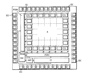
Referring to Fig 1, this illustrates the so-called floor plan
of the device. The device consists of an array A of programmable
analogue core cells CL each of which contains dynamic analogue
circuitry that requires refreshing to maintain its circuit
configuration and component values. Configuration data is held in
an on-chip 4,800 bit static random access memory RAM. This
configuration data source is continuously read to provide the
refresh function.
Configuration data which is stored in the random access memory
RAM, can be reconfigured from an external source in order to
implement new circuits within the array as required.
The random access memory RAM can be battery backed to provide
retention of circuit configuration data after power down if
required. The small back-up battery could be incorporated into the
integrated circuit packaging.
CA 02039424 1994-02-26
- X039424
Circuit configuration data is accessed to configure internal
interconnect sequential selection of the core cells CL by means of
programming shift registers PSRH and PSRV under control of a
control circuit CC. This configuration data is supplied to the
interconnect resources and programmable resources in digital form
over first data paths DD. Component values, stored in digital form
in the random access memory RAM, are supplied to programmable
resources over second data paths AD in analogue form via a
digital-to-analogue converter DAC. Each programmable resource has
a separate addressable sample and hold circuit (eg swtiches M1 and
M2, together with the analogue storage circuit N/STR and P/STR) and
configuration data is written to each sample and hold circuit
sequentially.
Although in the present exemplary embodiment the programming
shift registers PSRH and PSRV, digital-to-analogue converter DAC,
random access memory RAM and control circuit CC are shown on the
semiconductor integrated circuit with the array of cells it is
quite feasible for these components to be included on a separate
I.C. if required.
The sample and hold circuit (N/STR, P/STR) controls a
programmable voltage dependent resistor and each resistor is
individually compensated to allow for manufacturing tolerances and
temperature variations. Each programmable resistor is implemented
as a pair of complementary MOS transistors. Each transistor of the
pair has associated with it a second matched transistor that forms
part of a control voltage feedback loop.
CA 02039424 1994-02-26
-14- ~039~24
Capacitors are fabricated in values of 5E-12 farad. The value
of these capacitors is then multiplied in each case by two
impedance converters to a final value of 5E-9 farad. Each stage
(x33) consists of a buffer and two programmable resistors.
Within the array there are twenty eight basic cells BC1 and
BC28 and twenty one enhanced cells EC1 to EC21 (see Fig 2). Each
basic cell BC (Fig 3) consists of one general purpose operational
amplifier OA, four programmable resistors p/res and two
programmable capacitors p/cap. Each enhanced cell EC (Fig 4)
consists of a high speed operational amplifier OA, four
programmable resistors p/res, two programmable capacitors p/cap,
and one voltage dependent resistor VDR which can serve as an
analogue switch. Both the basic cells BC and the enhanced cells EC
have an inverting input IIP and a non-inverting NIIP and each
incorporates bias voltages BS together with voltage reference
sources VREF. The output OP is taken from each cell by way of the
operational amplifier OA. Each enhanced cell operational amplifier
OA may also be used as a comparator, linear integrator, or as a
multiplier when used in conjunction with the voltage dependent
resistor or analogue switch. This is particularly useful for
companding, gain control and modulation. Fig 10 shows a circuit of
a core cell operational amplifier which is generally of known
standard type incorporating MOS field effect transistors such as
MOSN and MOSP and has a non-inverting input NIIP, an inverting
input IIP and an output OP. VSS and VDD represent the voltage
supply and BS represents a bias voltage.
CA 02039424 1994-02-26
_15_ i~o~~~ :~
Using the voltage dependent resistors VDR in the enhanced
cells EC, external voltages ECV can be used by way of the voltage
dependent resistor node VDRN (see Fig 7) to control internal
circuit responses within the enhanced cell EC. For example, using
the array to implement a twenty channel graphic equaliser, external
potentiometers would not carry audio signals to and from the array,
only the control voltages.
INTERCONNECT
While each cell can be configured for the required circuit
function by programming internal resistors and capacitors and
connecting resources together over signal paths using pass
transistors PT, within the array there is a global interconect
system comprising metal interconnect lines which are used for
interconnecting cells over long distances within the array i.e. not
a neighbouring cell. Local connections can be effected through a
local interconnect system, where the output of each cell is
interconnectable to each input of its neighbours within the array.
Fig 5, Fig 6 and 7 is an illustration of the global interconnect
connectivity and the local interconnect arrangements for a basic BC
and an enhanced cell EC respectively. Fig 8 shows details of the
interconnect switch circuits IS.
Each interconnect resource is physically connected to each
cell using a pair of P and N channel pass transistors controlled by
a switch storage means in the Form of a static random access memory
SRAM. Fig 9 is an illustration of a pass transistor TR and its
CA 02039424 1994-02-26
-16-
associated random access memory SRAM forming a programmable switch
circuit. Data busses or switch control paths, forming part of the
previously mentioned first data paths, for controlling this switch
circuit, are designated D and D (see Fig 5). Each switch may be
selected by means of the line SEL. The connections IN represent
the interconnect nodes.
Cells within the device are embedded in a network of
interconnect resources and switching blocks. Each cell BC (see Fig
5) has associated with its two signal inputs IP1 and IP2 three
switch blocks IS1, IS2 and IS3, two IS1 and IS2 capable of
connecting locally to other cells (adjacent cells AC) and one IS3
capable of connecting to a global bus resource HB and VB. The
output OP of each cell directly connects to adjacent cell switch
blocks and in addition connects to a switch block ISO capable of
routing output signals onto a global bus resource HB and VB.
PROGRAMMABLE RESISTORS
A programmable resistor consists of voltage dependent
programmable resistor elements, each element consisting of a pair
of complementary MOS transistors.
Fig 11 and Fig 12 show the general arrangement for programming
each resistor element. It should be noted that in Fig 12, the
portions of circuitry from Fig 17 and Fig 18 which are shown, have
corresponding designations for the various components for the
referenced figures.
CA 02039424 1994-02-26
-17- ~0~9~'~4
Referring to Fig 11, N/CC and P/CC are both differential
amplifiers, while PR1, PR2, PR3 ... each comprise a programmable
resistor network R/BLK, Fig 12, Fig 13. Each programmable resistor
network has associated with it two analogue storage nodes N/STR and
P/STR (Fig 12). Each core cell (BC, EC) contains two differential
amplifiers which sequentially set the correct control drive voltage
for the voltage dependent programmable resistors. The analogue
storage nodes N/STR and P/STR store the control drive voltage for
the programmable resistor enabling the differential amplifiers N/CC
and P/CC to set other programmable resources. The circuit details
of the differential amplifiers are shown in Fig 27 and Fig 28.
Fig 14 and Fig 15 illustrate the basic 'P' and 'N' type
programmable resistor elements respectively. Each resistor element
is capable of providing thirty two resistor values within a 2:1
range, for example lOkohms to 20kohms in 32 steps e.g. lOk 10.31k
10.62k etc...
Each programmable resistor is implemented (see Fig 13) as six
pairs of 'P' and 'N' resistor elements N/RE1, P/RE1 to N/RE6, P/RE6
ranging in value between lOkohms to 640kohms. Each element is
connected in parallel with the previous element and is twice its
value, for example lOk to 20k, 20k to 40k etc....
Referring now to Fig 20 which illustrates the basic
requirements for selecting a particular core cell CL in an array
A. Firstly, the appropriate row is selected, and consequently a
particular constant current CCS, by select signals SS from the
CA 02039424 1994-02-26
-18-
~0~9424
shift register PSRH, whereupon a specific current level, relevant
to a particular desired resistor within a particular range of
values, is programmed .into the selected constant current source CCS
by way of the second data paths AD by means of the digital-to-
analogue converter DAC which has been programmed from the random
access memory RAM (Fig. 1). This serves as one coordinate
reference signal within the array. Secondly, the shift register
PRSV provides an appropriate column select signal comprising enable
signal EN and a select signal SEL to serve as the other coordinate
reference signal within the array. The particular enable signal EN
and select signal SEL together (SEL/EN) are arranged to select one
of the resistors (PR1 to PR4) to be programmed by the current from
the constant current source CCS. This is achieved during the
programme process whereby one pair of resistors from the six pairs
of resistors in the resistor network of the selected resistor is
selected by cell configuration data from the data bus DBB forming
part of the first data paths, and which is stored in the random
access memory RAMB (see Fig 14 and Fig 21 and Fig 22). Resistor
elements not selected are switched-out of circuit.
Referring now to Fig 21 and Fig 22 which should be arranged as
shown in Fig 23, the general arrangement of a basic cell BC is
shown with four programmable resistors PR1 to PR4 (P/res, Fig 3)
each taking the form of a network R/BLK as shown in Fig 13.
CA 02039424 1994-02-26
-19- ~039~~4
Each resistor comprises the six pairs of resistor elements
N/RE1, P/RE1 to N/RE6, P/RE6 previously mentioned and each has an
associated analogue store N/STR, P/STR as previously indicated.
Any pair of resistors and consequently a particular resistor value
range can be selected by data on data bus DBB which is stored in
the random access memory devices RAMB. Switches SWA and SWB (Fig
14 and Fig 15) are caused to operate to switch-in the appropriate
resistor pair. The effect of this switching is shown
diagrammatically in Fig 17 and Fig 1$ where DRIVE (10, 19; Fig 16)
SET (10, 19; Fig 17, Fig 18) input can be controlled by switching
switches SWA and SWB.
Referring again to Fig 21 and Fig 22, the horizontal (CCS,
REF7) coordinate reference and the vertical {EN, SEL) coordinate
reference are each shown together with differential amplifiers N/CC
and P/CC previously referred to which serve the whole cell, and
provide the necessary DRIVE and SENSE signals (ND/S, PD/S) for
setting the resistor element to the desired value in the selected
range.
Following this procedure where the shift registers PSRH and
PSRV are progressively advanced the various components in all the
cells can be programmed and set successively. For instance row one
is firstly selected then row two and so on for each successive row.
followed by the successive selection of each of the columns. each
component being programmed and set in selected cells on a
successive basis.last and is twice its value, for example, lOk to
20k, 20k to 40k etc...
CA 02039424 1994-02-26
2° ~0~942~
During programming one pair out of six is selected by the data
stored in the random access memory RAMB. Resistor elements that
are not selected are turned off.
A further example of the programmable resistor circuit is
illustrated in Fig 16. N/CC and P/CC are the differential
amplifiers, while N/RE and P/RE are both programmable resistor
elements within a network. By referring to Fig 16 and Fig 17, it
will be seen that the output of differential amplifer N/CC is
arranged to drive (SET, 10) the gate of an 'N' type transistor M4
through the switch formed by transistors M1 and M2. The source
connection of M4 is held at a reference potential of 1.5 volts (REF
5) and the drain of M4 is connected to transistor M5 which is in
turn connected to a constant current source at terminal (REF 7).
The junction of M4 and M5 is connected to the non-inverting input
(17, SENSE - Fig 28) of the differential amplifier N/CC through
transistor M33 (Fig 17), the inverting input (26, REF 3 - Fig 28)
to the differential amplifier is connected to a reference potential
of 2.5 volts.
The programmable resistor is implemented with transistor M3.
The gate drive for M3 is derived from the gate potential of M4,
which is part of a negative feedback path around differential
amplifier N/CC (Fig 17, Fig 28).
To programme the resistor to the required value, the constant
current source CCS (Fig 20) is adjusted to the appropriate current
setting (O.lmA for lOk ohms O.OlmA for 100k ohms etc.) until the
CA 02039424 1994-02-26
-21-
negative feedback path has stabilised. The stable condition for
the differential amplifier is achieved when both of its inputs are
at the same potential (2.5 volts). At this point the voltage drop
across transistor M4 is equal to 1 volt (2.5 - 1.5, Ref 5).
Transistor M4 will then have a drain current equal to the constant
current source. The potential at the gate of transistor M4 is now
at a level for the required conductance of transistor M4. As the
gate potential of transistor M4 is also connected to transistor M3,
transistor M3 will also be programmed or set to the required
resistance.
Referring to Fig 13, Fig 17 and Fig 18, it will be appreciated
that connected in parallel with transistor M3, and 'N' type
transistor, is a 'P' type transistor M12. Transistor M12 with its
associated circuitry perform a similar function to transistor M3
and its associated circuitry except that transistor M12 will have
an inverse characteristic with respect to transistor M3. To
implement a programmable resistor both transistors are necessary to
ensure a linear transfer function.
ANALOG STORAGE MODE
Once the required drive for transistor M4 is established
transistors M1 and M2 are switched off, the gate potential of M4 is
maintained on capacitors C1 (200 fF) and (C2 400 f)F until it is
refreshed lE-3 seconds later. Two transistors are required to
switch the gate drive to M4 in order to prevent corruption of the
potential stored on C1 and C2 due to capacitive coupling of the
CA 02039424 1994-02-26
_22_ i~~~'~~r~'4~
driving signals on the gates of the switching transistors M1 and
M2.
The potential applied to the gate of transistor M4 is also
applied to a capacitor storage circuit formed around transistors M6
to M9 and capacitors C1 to C2.
N/STR, P/STR illustrates the storage circuits (see Fig 1'7 and
Fig 18). Transistors M8 and M9 form an inverting amplifier. The
simple amplifier is only capable of operating near half the supply,
transistors M6 and M7 provide a voltage level conversion function
to enable the storage circuit to operate at voltages approaching
VDD. The 'P' type programmable resistor element requires a storage
circuit that can operate near to voltage VSS.
Fig 19 illustrates the discharge characteristic of the storage
circuit verses a simple capacitor circuit of the same capacitance,
the improvement in the retention period that an acceptable voltage
can be maintained can be clearly seen.
The storage circuit is required to maintain this analog
potential while the programming circuit is setting other resistors
on the array. The active storage circuit generates the inverse of
the normal exponential discharge characteristic of a capacitor and
resistor. The storage circuit also resists modulation of the gate
voltage caused by capacitive coupling between the gate and the
source or drain regions of transistor M3 or transistor M12.
CA 02039424 1994-02-26
- i~~~~~~~,.~
The capacitor used For storing the gate drive for transistors
M3 and M4 has to be able to hold the charge without significant
degradation until the next refresh period (lE-3 sec). Any
variation in the potential across the capacitor will result in a
change in the resistance of transistor M4, but more importantly
transistor M3. This could have a catastrophic affect on the users
circuit. If the circuit implemented is a filter the
characteristics could change, i.e. a change in gain or phase. If
the circuit has a high gain stage it could result in oscillation.
The effect of a changed resistance in transistor M4 is not the
same as a fixed resistor tolerance as the resistance will change
dynamically at the refresh rate. This will introduce a frequency
of lKhz to the circuit node to which it is connected.
PROGRAMMING
Referring again to Fig 20 which illustrates the global
programming circuit. A digital to analog converter DAC generates a
voltage proportional to the required resistance or capacitance for
each component in the core cell. The output of the
digital-to-analogue converter DAC is converted at CCS to a current
which is applied to the global load (REF '7) to provide the selected
cell with the appropriate programming current. The digital-to-
analog converter DAC is driven by the on-chip random access memory
RAM (see Fig 1), which contains configuration data and component
values in digital form. It should be noted that all the
programmable components in the array are sequentially refreshed to
maintain the correct individual component values.
CA 02039424 1994-02-26
-24-
20394~~
PROGRAMMABLE CAPACITORS
Referring to the drawings and particularly to Fig 24 which
illustrates a programmable capacitor circuit, it should be
appreciated that capacitors are implemented using a capacitive
multiplier technique. Programmable capacitors comprise essentially
three elements, a capacitor C1 and one or two capacitor multipliers
M1 and M2. These are shown connected between nodes CN1 and CN2.
As it is not possible to fabricate one hundred 5E-9 Farad
capacitors, a small capacitor C1 (5E-12 Farad) is fabricated and
the equivalent of the required capacitor value is then generated by
a process of impedance conversion.
The 5E-12 Farad capacitor C1 is connected to the output of a
first buffer circuit B1. Programmable resistors RP1 and RP2
(resistors whose values may be changed as required) are connected
in series between the input and output of the first buffer circuit
B1, an output being taken from the junction between the first and
second programmable resistors. By this arrangement of components,
the ratio of the set values of the two programmable resistors RP2
and RP1 determines the amount by which the capacitor (Cl) value is
2~ multiplied.
The set value of resistor RP2 is higher than the set value of
resistor RP1, therefore, the effect at the junction of resistors
RP1 and RP2 is multiplication, and an overall effective capacitance
value equal to (RP2/RP1} x C1. The effective capacitance at the
junction of resistors RP1 and RP2 is further multiplied by the
CA 02039424 1994-02-26
-25- ~039~'~4
second stage multiplier M2, including programmable resistors RP3
and RP4 and a buffer B2. Thus, the final effective capacitance at
the junction of resistors RP3 and RP4 approximates to (RP2/RP1) x
(RP4/RP3) x C1. This second stage multiplication is necessary if
higher value capacitors are required in order to avoid the effects
of parasitic capacitance present in the higher value programmable
resistors required to produce a higher value capacitor.
Programmable resistors RP2 and RP4 are utilised for
programming the final capacitance while resistor RP1 is driven by a
reference signal CCV (see Fig 24 and Fig 25) to compensate for the
manufacturing/processing variations of capacitor C1.
The main drawback of this type of circuit is that high Q
capacitors cannot be produced. For most applications for capacitors
produced in this manner, however, this is not a major problem since
the capacitor multiplier has a series resistance that approximates
to the value of resistor RP3.
The capacitor compensating circuit shown in Fig 25, including
an external section EXT and a semiconductor integrating circuit
section SIC, is arranged to provide a capacitor multiplier voltage
~ reference control signal CCV which controls the programmable
resistor RP1. In this way, the variations in oxide thickness of
the 5E-12 farad capacitor C1 are automatically compensated for.
A supply voltage is applied to terminal SP, and in operation
it is arranged for a timing circuit to compare the time constants
of two separate but substantially identical capacitor/resistor
CA 02039424 1994-02-26
_26_ G~~~~r
circuits. One time constant circuit employs an accurate external
capacitor ERC1 of 5E-9 farads in series with a known accurate
value, external resistor ERR1 and the other time constant circuit
employs an internal capacitor IC (of the type shown in Fig 24) of
5E-9 farad (generated by multiplication of an internal capacitor of
5E-12 farads) in series with an external resistor ERR2.
It is arranged that the two capacitors IC and ERC1 are charged
and discharged repeatedly by switching the switches SW1 and SW2
under control of clock signals DCLK which is the clock signal CLK
delayed by the delay DL. The connectors REF4 on the switches SW1
and SW2 are conveniently connected to zero volts.
At the time of the delayed clock signals DCLK, the comparator
CP repeatedly compares the voltages across each of the capacitors
IC and ERC1 to determine which of the capacitors is charging up the
fastest and the resultant output from the comparator is
latched/stored by the 'D' type flip-flop DFF.
At the actual time of the clock signals CLK, the output Q from
the flip-flop DFF (the previous signal comparison output
corresponding to the time of the immediately preceding clock signal
CLK) is output to an integrator circuit INT comprising a further
external capacitor ERC2 and a further external resistor ERRS, and
this integrates successive output signals from Q. The output from
the integrator circuit IC is fed through a second buffer circuit
BUF to provide a reference signal CCV (an analogue signal) which
CA 02039424 1994-02-26
~'~39~~4
provides a direct control for varying the value of resistor RP1 in
the multiplier M1, and thereby change the ratio RP2/RP1 and hence
the effective value of the capacitor IC.
It should be understood that the analogue signal CCV requires
conversion to an equivalent digital form to be effective on the
circuit to change the value of the resistor RP1. This may be
achieved by a suitable analogue-to-digital converter ADC inserted
between the output of the second buffer circuit BUF and the input
to the circuit PRC for controlling the programmable resistor RP1.
Thus, in operation, an iterative process takes place whereby
the integrator circuit continuously changes the analogue signal CCV
which in turn changes the value of resistor RP1 and in turn the
effective value of the internal capacitor IC. This process
continues until the correct value capacitance is attained.
Explaining this further, if the internal capacitor IC charges
up quicker than the external capacitor ERC1, then the reference
voltage CCV is reduced. This has the effect of increasing the
value of the internal capacitor IC by varying the ratio of the
resistors RP1 and RP2 in the multiplier M1.
Alternatively if the external capacitor ERC1 charges up
quicker than the internal capacitor IC, then the reference voltage
CCV is increased. This has the effect of decreasing the value of
the internal capacitor IC by varying the ratio of the resistors RP1
and RP2 in the multiplier M1.
CA 02039424 1994-02-26
_28_ ~039~'~24
Referring now to Fig 26 which shows a detailed circuit diagram
of a high impedance input, low impedance output unity gain buffer
stage as employed in the multipliers M1 and M2 for first buffer
circuits B1 and B2, the input is designated IPN and the output is
designated OPN. These nodes are designated identically in both Fig
24 and Fig 25.
The buffer circuit comprises three P-type MOS transistors.
TR1, TR2 and TR3 and three N-type MOS transistors TR4, TR5, TR6 and
TR7. VSS and VDD represent the supply voltage for the circuit
while REF1 represents a suitable reference bias voltage.
Fig 29 shows the details of the peripheral programmable gain
input/output circuit IOC (Fig 1). Each cell employs operational
amplifiers OAI, a random access memory, RAM1 a programmable
resistor P/RES and a transistor switch TR1 serving as a pass
transistor. ECN represents the bond pad connection while IPA
represents the input to the array whereas OPA represents the output
from the array. REFV represents a reference voltage.
LOWPASS FILTER CIRCUIT EXAMPLE
A second order low pass filter is illustrated in Fig 30. The
same circuit implementation on the array is illustrated in Fig 31.
In Fig 31, those components and portions of circuit not used, i.e.
switched out, are shown in dotted outline.