Note: Descriptions are shown in the official language in which they were submitted.
PROTECTIVE RELAY OF A MEDIUM VOLTAGE ELECTRICAL MAINS SYSTEM
. ,. _ _ '
BACKGROUND OF_THE INVENTION
The invention relates to a protective relay of a medium voltage
electrical mains system, located in a case comprising at least
one conducting part, and comprising inputs to which analog input
signals representative of electrical parameters of said mains
system are applied, an electronic processing unit of the input
signals and a reducer transformer, assoclated with each input,
comprising a primary winding connected to said input and a
secondary winding connected to the electronic processing unit.
The electronic circuitry, and more particularly -the digital
electronic circuitry is very sensitive to variations of electro-
magnetic fields produced by a medium voltage environment. The
introduction of electronic trip devices, notahly microprocessor-
based trip devices, for protection of medium voltage electrical
mains systems, gives rise to problems due to the influence of
electromagnetic disturhances on the electronic circuitry of the
trip device.
SWMMARY OF THE INVENTION
_
The object of the invention is to limit these disturbances with
simple, inexpensive means occupying little space.
According to the invention this objective is achieved by the
fact that the primary winding of a reducer -transformer, formed
by a conductor connecting two terminals of the associated input,
is shielded by a non-magnetic material, said shielding heing
connected at its two ends to a grounded conducting part of the
case.
This shielding, formed preferably by a braided strip made of
non-magnetic material, constitutes a very inexpensive Faraday
cage of small size, limiting the electromagnetic disturbances,
by capacitive coupling, and the disturbances due to the low
frequency magnetic ~ield liable to affect the electronic
processing unit.
According to a preferred embodiment said conducting part, which
is for example metallic, is formed by an external wall of the
case on which said inputs are arranged.
The primary windings of all the reducer transformers of the
relay, whether they be current or voltage transformers, can be
shielded. It is however possible to limit the shielding to the
primary windings of the current transformers while still
obtaining satisfactory results.
BRI~F DESCRIPTION_OF THE DRAWINGS
:
Other advantages and features will bec:ome more clearly apparent
from the following description of an lllustrative embodiment of --
the invention, given as a non-restrictive example only and
represented in the accompanying drawings, in which :
Figure 1 is a schematic representation of a relay according to
the invention;
Figures 2 and 3 respectively illustrate a current signal input
and a voltage signal input.
DESCRIPTION OF THE PREFERRED EMBODIMENT
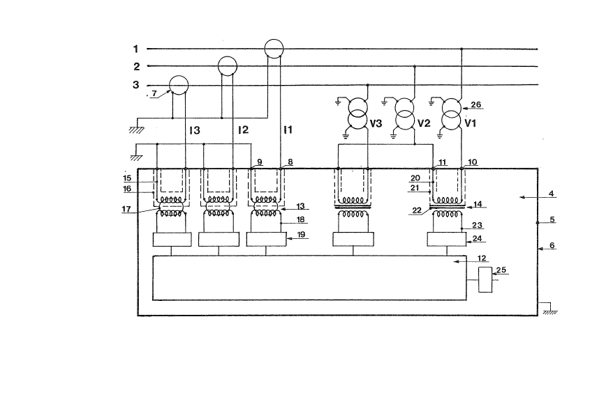
In figure 1, a relay designed to protect a medium voltage three-
phase electrical mains system, comprising three phase conductors
1, 2 and 3, comprises an electronic trip device ~.
3 ~ } ~
The trip device 4 is located in a case 5 one external conductlng
wall 6 of which ls grounded. The wall 6 is a metal wall but can
be formed by a wall made of plastic material charged with a
conducting material or covered with a metallic paint.
Analog input signals, respectively representing the currents Il,
I2, I3 flowing in the conductors and voltages Vl, V2, V3 of the
mains system conductors, are applied to inputs of the trip
device. An inpllt signal of the current Il, I2, or I3 is obtained
conventionally by means of a current transformer 7 whose primary
winding is formed by the conductor involved and whose secondary
winding is grounded by one end and connected to a first terminal
8 of the associated input by the other end. The second current
input terminals 9 are all grounded. Likewise, a voltage input
signal Vl, V2, V3 is obtained by means of a voltage transformer
26 whose winding is connected at one end to the conductor
involved and is gxounded at the other end. The secondary of the
transformer 26 is connected at one end to the terminals 10 for
Vl and V3 and to the terminals 11 for V2, the other end of the
secondary of the transformer 26 being grounded.
The input terminals 8, 9, 10, 11 are preferably located on the
external metal wall 6 of the case.
The inp~t currents and voltages are too high to be processed
directly by the electronic processing unit 12 of the trip
device. To give a non-restrictive example, the current signals
generally have an intensity in the order o~ a few amps,
typically 1 to 5A, whereas the voltage signals can be in the
order of a hundred volts. A reducer transformer is therefore
connected between each input and the electronic processing unit.
Current reducer transformers 13 are associated with the current
inputs 8, 9, whereas voltage reducer transformers 14 are
associated with the voltage inputs 10, 11.
.. : ~ ,
: ', ,
.
The primary winding 15 of a current reducer transformer 13,
connected to the terminals 8 and 9 of the associated input, is
shielded over its whole length by a shielding 16 made of non-
magnetic material, preferably formed by a braided strip, as a
non-restrictive example, a tinned copper strip. The two ends of
the shielding are connected to the grounded metal wall 6 by any
suitable means, for example by means of a self-tapping screw or
a nut and bolt system. Figure 2 illustrates in greater detail
the shielded conductor 15, 16 passing through the toroidal core
17 of the current transformer. The secondary winding 18 of th
transformer 13 is connected to a shaping circuit 19 whose output
is connected to an input of the electronic processing unit 12.
In the embodiment represented in figure 2, the primary 15 of the
current transformer 13 forms a single turn passing through the
toroid 17. Naturally if the input current is lower, the primary
15 can comprise several turns.
Likewise, the primary winding 20 of a voltage reducer
transformer 14, connected to the terminals 10 and 11, is
shielded by a shielding 21 made of non-magnetic material.
According to a preferred embodiment represented in figure 3,
only the part of the primary winding 20 going from the input
terminals 10 or 11 to the beginning of the winding on the
transformer core is shielded. The turns are not shielded and the
shielding 21 is connected, by any suitable means, to both the
metal wall 6 and to a grounded insulating electrical shield 22
separating the primary 20 and secondary 23 windings. The
relative dimensions of the shielded part of the conductor 20 and
of the non-shielded part must be such that the shielding
nevertheless forms a Faraday cage. To serve as an example, this
type of shielding is sufficient in practice, for a voltage
transformer 14 in which the transverse dimension covered by
turns is in the order of one centimeter, whereas the length of
the conductor going from the input terminals 10 or 11 to the
part forming the turns is in the order of ten centimeters.
The secondary winding 23 of the transformer 14 is connected to
the electronic processing unit 12 by means of a shaping circuit
24.
The shielding according to the invention is more particularly
suitable in the case of a trip device 4 whose electronic
processing unit comprises a microprocessor, the analog input
signals being multiplexed then transformed into digital signals
before being processed by the microprocessor.
The electronic processing unit 12 notably performs protection
functions and can transmit tripping and closing orders to a trip
relay represented in schematic form by 25 in figure 1.
:
'
: ::......... . .