Note: Descriptions are shown in the official language in which they were submitted.
8 ~ 51:~ ~7q ~70~ rlcE l roY Tr~ns 1~. 01, 22~ 91 1~ 2 003
20397~5
~ode: 232-6573
DATA PRo OE SSING SYSTEM AND ~ETHOD FOR
~ONTROLLIN~; THE I~l~TER AS WELL AS A CPU BOARD
Th~ invention relata~ to a data proaessing sys~em and a
method ~or controlling th- latter with the da~a processing sy~tem
having a central processing unit (CPU), a main memory and a
~ys~em bus which can b~ connected to the main memory and other
functional unit~. The ihvention also rela~e~ to a CPU board for
~ d~ta processing sy~em in which the ~PU i~ mount~d on its own
board.
Normally, th~ CPU, main memory and ~he input/output unit~
~I/O unit~) or thQir con~roller~ are each on a board, al50
r-ferr~d to as a card. All ~unqtional unit~ connected to the
~y~t~m bu~ are thus controlled c~ntrally by the c~ntral process-
lng unit ~ CPU), e . g . ~y a micropro¢es or . A~ a r~sult, communi-
cation ~etween the func~ional unit~ and the CPU always take~
pl8c~ via the sy~t~m ~u~.
For example, if an I/O unit wi-heg to trans~er data with the
main mQmory, i.e., input data to th~ main m-mory or output data
from the main memory, ~h~ I/O unit Qnds a slgnal to th~ syctem
bus ~ on the ~asi~ of thi~ signal, the CPU i~ "ha}tcd" Yor a brlef
period o~ ti~ while th~ I/O unit i~ p~rmitted to directly access
the main memory, a proce a al60 refe~red to as DMA (dir~ct memory
acca~s ) .
since a great many direct acce~e~ are made to th~ main
m~mory, particul~rly during p-ak load op-ration, jam~ ~d long
w~iting p~riod- occur: thi~ iB due to th0 ~act that the ~y~tem
J~N 22 ' 91 12: ~19 512 479 6703 P~GE . ,303
8 51? 473 67EI~ ~lcEIr~oY Tr~nsl~. ~ 22, 91 1_:43 0~34
2~3~715
bua timing i~ standardized and therefore cannot be accelerated to
any ~peed, especially since all plug-in card on the sy~tem bus
mu3t adhere to certain invariable t~min~s.
An entire range o~ technique~ are known for the si~ultaneous
proce~ing of a~ many tas~s as possible in data proceQ~ing
systems. For example, so-called cache memories are used as
small, fa~t buffer~ and are pla~ed on the same board as the ~PU.
~he CP~ then outp~ts the da~a from the main memory via the system
bus and write~ the~- data to the fast cach~ ~-mory located on the
cPu board. If ~he CPU attempt~ to r-access ~hi~ dAta, it no
longer has to trans~er the data from the main memory via the
relatively slow ~y~tem bu~, but can directly acceos t~e fast
cache memo~y,
Due to advanced lntegration technology, it ha~ bacome
po~ible to place ~he CPU and main ~emory on a ~inqle board.
Since ~omm~nic~tlon betwean the I/O unit~ ~nd the main ~emory
continues to tak- place vi~ ~e syste~ bu~, the latt~r i~ bloaked
to the ~ain ~emory by requent DMA acGe3sos, i.e~ acce~e~ by I/O
units with direct acc~s, ~o that long wai~ing pexiod~ ~gain
04cur.
In contrast, the purpo~e of the ~nvention is to increase the
per~or~ance of the d~ta proce~ing syatem so that ~ many tasXs
a~ po~sibl~ can be proce~sed simultaneously and waiting periods
on the 6y8tem bu~ reduced.
This objectiv- i~ r-ached by th~ fact ~hat th- ~ain memory
can be dir-ctly conn-cted to the CPU; a first ~witching
meohahism, whic~ control~ the connectlon between the ~PU and main
memory, and a second switching mechanism, which control~ the
~onnection between the system bu~ ~nd the main memory, are
J~N 2Z ' 91 I Z: 50 51 Z 479 67133 P~GE . 004
8 - 512 473 67133 M~Elro~ Tran~l~. 01'22~91 12:44 005
203~71~
provided; the first and second switching mech~nismæ are intercon-
neCtQd BO that only one of the two ~witching ~echa~is~s can
release ~he ~onnection between the cPu or th~ syste~ bu~ and the
main memory.
~his make~ it posstble to acces~ the ~ain ~e~ory from either
the CPU or the sy~tem bu~, and the main memory need be blocked to
the opposite side only for th- period in which the memory i6
actually being accessed, but not ~or the ontîr~ a~ce~ cycle.
The ~act that a fir~t ~uffer, wh~¢h $~ controllRd by the
first ~witching mechani6m, i~ provided between the CPU and main
memory and a second buffer is located between the ~ystQm bu6 ahd
main memory Rn~ures that data 18 ~orrectly transferred betwe~n
the ~PU and main memory as woll as b-twe-n th~ ~y~tsm bu8 and
main memory.
The ~ain memory, ~h- ~irst and second sw$tching m-~hanisms
and the ~ir~t an~ ~econd buff~r~ should ~- mounted on the ~ame
~oard a~ th- cPu.
In an additional vQrsion of the inventio~, one o~ more I/0
unit~ without dtre¢t memory access are provid-d: they can be
d~ec~ly connected to the CPU via a ~PU bus, and the CPU can be
connect~d ~ither to the m~in memory or to one of the I/0 units
without direct memory acce~. Thi6 makes ~t p~ssible for the c~u
to directly acce~s I/0 unit- evon lf the syste~ bus is bloc~ing
the path ~etween the ~ain ~e~ory and a DMA unit. As a result, it
i~ possiblo to further in~rease th~ performanco o~ the d~ta
proc~ssin~ sy~tem.
The ~PU board according to th- invention, which i~ described
in Claim~ 7 through 1~, can be ~old ~eparately from th~ data
JRN 22 ' 91 12: 51 512 479 6703 P~GE . 00'.
8 512 4~q ~71~3 r1~ 1 roY Trans l ~ Z, ~l 12: 44 006
203971~
proco~ing ~y~tem a~ lonq a~ compatibility with the appropriate
data processing syBtQm i~ guaranteed.
The method acco~di~g to the invention is ~escri~ed ln Claim~
12 through 16.
A ver~ion of the invention i~ d~scribed in greater detail on
the basis of the drawing~.
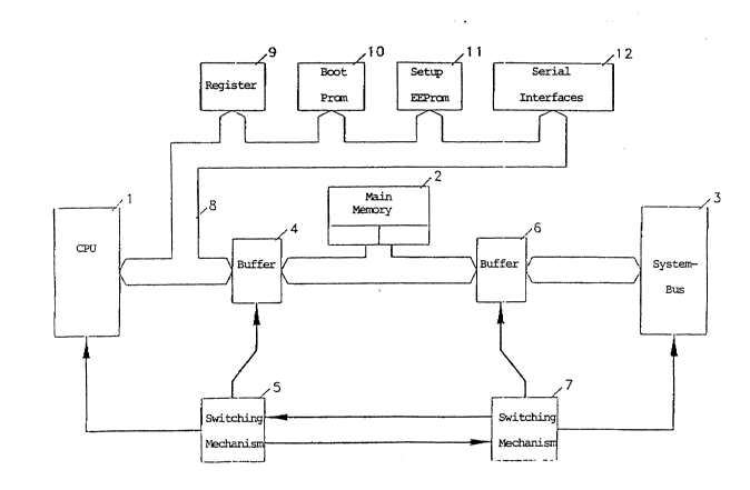
Fi~ure 1 show~ a ~ahematic block diagram of a data pro~ess-
ing ~y~tem according to the invention;
Figure 2 ~hows a flowchart ~or illu~trating the operation of
a f ir~t switching mechanism;
Flqure 3 showo a ~lowchart for lllustrating th~ operation of
a ~econd ~witching me~hanlsm.
A~ shown in Figure 1, the data proce~sing system according
to the invention has a central proce~ng unit (CPU) (1), a m~in
memory ~2) and a system bua ~ 3 ) .
Th~ CPU (1) ~ conn~cted to the main memory (2) vla a first
buffer (4). The connection is then controlled via a ~ir~t
~witchinq mechanis~ (5).
Th~ main memory ~2) ~8 also connect~d ~o the system bus ~3)
vla a bu~f-r (~), and th~ connec~ion is controlled by a ~econd
switching moc:hani~m (7).
The data proce~sing system according to the invention also
h~s a ~PU bu~ (8) which conn~cts the cPu (1) to a number of I/O
unit8 w~thout dir~ct ~ccess, i.e. I/O unit~ wlthout DMA. The
v~r~ion illu~trated con~i~t~ of a register set (~) ~ a boot PROM
(lo~ ~nd a setup EEPROM (11~ a~ w~ll AS additional s~rial inter-
f~ces (12~.
I~O units ~9) through (12~ a~e typical I/O units which ar~
conn-cted to the ~y~tem bus (3) in known d~t~ proce~ing ~y~tems.
JQN 22 ' 91 12: 51 512 479 6703 P~IlJE . 006
8 512 47~ 670~ l~lcElroY Transla. 131'22,91 l~:45 1a07
203971~
ThU~, registor set (9) normally has an interrup~ controller, a
cloc~-pul~e generator and a real-tim- clock. A~ usual, boot PROM
(10) and ~et EEPROM (11) contain the functions for starting the
syst~m, configuration data, hardwar--related functions, diagno~-
tic programs, 6elf-test programc, etc.
Th~ serial interfacea (12) include, for example, eight
interrupt-capable serial lines connect~d to the system con~ole,
terminal~, printers, mod~ms and ~ ar device~. In addition, a
~lo~ting-point unit (not illu~trated) can be connected in the
usual m~nner to th- CPU bu~.
~ 11 component~ ~llustrated in Figur~ 1 should be placed on
th- CPU ~oard~
operation of the d~ta proc-s~ing ey~tem according to the
inv~ntion is described below.
Since the CPU (1) or I/~ unit~ with direct ac~ess (DMA
units), which are conn~ctod to the syctem bus in the usual manner
and ~re not illu3trat~d in Figur- 1 for reason~ of alarity, can
ACC-~ th~ main memory (2) ~imultaneou~ly via ~h~ ~y~tem bus ~3),
teahnical implemen~ation r-quires the u~e of two switching
~ech~n~m~ which control the timinq in the appropriate system
part.
The $irst switching ~echanis~ (5) control~ all CPU-related
proees~es auch as acces~e~ from the CPU (1) to the main ~mory
(2) dnd ~o the I/O units without DMA, which are marXed by refer-
enc~ number~ (9~ throug~ (12) in Figur~ 1.
The second switching ~echanis~ (7) controls proces~ing o~
DMA reque~t~ f~om th~ sy~te~ bus ~3), the actual accesse6 by DMA
unit~ a~ well a~ aaaesses from the CPU (1) to ~he sy~t-m bus (3).
J~N 2Z l9l 12:52 512 479 670~ P~GE. 007
8 - 512 47~ 6703 McElr~Y Transla. 01~22~91 12:45 008
203971~
The first switchinq mechani~m (5) and the second ~witching
mechanl~ (7) ~ork in so-called handshaking mode, which guaran-
tee;~ ~utual blocking wh~n acc~ss request~ occur at the same time.
Operation of tho fir~t ~witching mechanism (5) is descrlbed
in gr-ater detail below on the ba~is of ~igure 2.
Firstly, the fir~t ~witching ~echani~m (5) i5 in a wait
st~tu~ ~100). In ~tep (101~, the ~ystem askQ whether the CPU ~1)
is to acce~s the main memory ~2). I~ it i~ not to do this, the
~ystem ~sks in step (102) wh~er a request ~egarding or an
interrupt from one of the I/O units without DMA marked by refer-
ence numb~rs (9) through (lZ) in Flgure 1 is present. If it is
pre~4nt, the re~ue6t or interrupt i8 proc~ss~d in step (103).
If the sy~tem det~rmines in step (101) that the main memory
(2) i~ to be acc~-ed, ~wltahing ~echanism ~5) assigns the maîn
memory (2) in ~tep ~104) and send~ a r-levant a~ign signal to
switching mechani~m t7)~ If the sy6tem deter~ines in step (105)
that the main memory (2) is busy, i.e., an acce~ from a DMA unit
vi~ the ~y~tem bus (3) ~o th- main memory (~ preseh~ it
wait~ until the main memory ~2) i~ ~re~. In st-p (106), th~
~mory operation i~ then carried out, and buffer ~4) 18 con-
trolled by switching mechanism ~5). At the end of the memory
operatio~, the main memory (2) i9 again rele~sed in step (107)
and an approprlate relea~e signal ~ent from switching m~chanism
(5) to switching ~echani~m ~7).
Operation of the ~econd ~witching mechanism (7) is described
in greater detail b-low on the ba~ f Figure 3.
~ irst~y, the 6econd ~witching mechani~m t7~ n a wait
~tatu~ (200~. In step (201), th~ s~t~m asks whether a request
~rom a DMA unit via the ~y~te~ bu~ (3) is pr~sent. If one is
Jf~N 22 ' 91 IZ: 53 512 479 6703 PflGE .00a
8 ~12 ~17~ 1cElroY Transl~. 01~'Z/91 12:46 009
203~
pre~ent, ~witchinq mechani3m (7) send~ the DMA relea~e to the
~ystem bus (3) in st~p (202). A bidirec~ional connectlon is then
establi~hed ~rom swltch1ng m-chaniam (7~ ~ia the system bus (3)
to the ~MA unit connect-d to the #ySt~m bus ~3) and the first
part of t~e bu~ protocol i~ processed in ~tep (20~). Switching
mech~ni~m ~7) then ~signs the main memory (2) and send.~ an
appropri~a assign ~ignal to switching mechanism ~S). If t~e
sy~tem determines in ~tep (205) that the main ~emory ~2) is busy,
i.e., an acce~s fr~m the CPU ~1) to the ~ain memory (2) is pras-
ent, it waits until th~ main memo~y (2) is free. In ~tep (2063,
~h~ memory operation i~ then carried ou~, and buffer (6) is con-
trolled by ~witching ~echani~m (7).
At the end of tho m~mory op-ratlon, the main ~mory (z) i8
rel~a~d in ~tep ~207) and an approprlat- rsleas- signal is sen~
f~o~ switching mech~nism (~) to switching me~hanism (5). In step
(208), the second part o~ the bus protocol iJ thQn process-d
throug4 communication between switching meohanism ~7) and the DMA
unit.
The dQvice which can acce~s the main memory (2 ) i8 thus
determlned by the two fas~ switching mechan$sm~ (S) and ~7) whlch
co~unic~te with ~ach other and operate in handshaking mode.
Flgures 2 and 3 d$r~ctly $11u~trate that the main m-~ory 12)
i~ assigned only during t~- p~r~od of tim- ab~olutely necess~ry.
Thi~ p~riod is indi~ated by the broken lines and marked by the
ref~rence number (110) ~n Flgure 2 and by reference numb~r (210)
in Figure 3.
During the re~ainin~ period, i.~. the r~maining processing
time for a DMA acce~s ox a CPU acce~ to the main memory or even
during CPU acce~s to ~h~ I/O units ~ithout DMA ac~ess marked by
J~:IN 22 ' 91 12: 53 512 ~179 ~703 P~GE . 009
51- ~ Ac- lroY Tr~ns l~ 31l~
2~3~7~ ~
reference nu~bers (9) through (12), the main memory can be
released and aQsigned for a new reque~t.
The version according to the lnvention prevents the main
memory from being assiqned during the entire standardized pro-
cessing time o~ a DMA access, which run~ from steps (201) to
~208) in Figure 3; instead it can b~ assigned only durinq the
ab601ute1y necessary period resulting from steps (204) to (207)
in Fi~ure 3. The time desi~nates as idle ti~e (steps 201 to 2~3
and st-p 20~ in Figure 3) between memory assignment (steps 204 to
207 in Figure 3) and standard proceseing time (step~ 201 to 208
ln Figure 3) can be u~ed for other purpo~es, e.g. for access by
ths CPU to the ~ain m-mory in order to n~st the actual memory
acc~s~es close t~gethcr in time.
As a ~urther way to increa3e system p~r~ormance, the cPu can
process reque8ts from I~0 unit~ wlthout DMA access during th~
time in which the nain memory i5 assigned by the system bus,
thereby permitting true paral}el processlng.