Note: Descriptions are shown in the official language in which they were submitted.
2039775
PARABOLA GENERATORS WITH AUXILIARY RESET FUNCTION
This invention relates to the field of parabola generating
circuits for use in correcting distortion of raster displays in
televisions, and in particular, to parabolic waveform generators
5 which exhibit enhanced immunity to vertical rate disturbances as
may be caused by operation of certain kinds of vertical deflection
circuits and enhanced immunity to distortion during channel change.
A theoretically correct scanned raster display in a television
apparatus is exactly rectilinear, with all the horizontal lines of the
o raster straight and parallel. In unidirectional raster scanning, of
course, the scan lines have a very slight downward inclination.
Several different kinds of distortion can result from either the
circuits producing the vertical or horizontal beam deflection
signals, or from the geometry of a projection television system.
15 Pincushion distortion is characterized by an inward bowing of the
raster. Pincushion distortion can be a problem in both direct view
and projection sets. Trapezoidal distortion is mainly a problem of
projection sets because all of the multiple projection tubes cannot
be aligned on the same projection axis. Convergence distortion is
20 characterized by a misregistration of corresponding points of the
respective rasters produced by the projection tubes of a projection
set.
One form of pincushion distortion is often referred to as
North-South pincushion distortion. The horizontal raster lines at
25 the top and bottom of the display are bowed inwardly toward the
center of the display by an amount which is greatest for lines at the
extreme top and bottom, and less approaching the vertical center.
Another form of pincushion distortion is referred to as East-West or
side pincushion distortion, and is characterized by the endpoints of
30 the horizontal raster lines varying in lateral position such that the
width of the horizontal raster lines is less at the vertical center of
the raster than at the top and bottom.
In a projection television apparatus, a color display can be
produced by projecting three separate rasters from monochrome
35 cathode ray tubes (CRTs) for the primary colors from different
locations, and overlaying the three rasters when projecting them
~,
2039775
. - 2 -
onto a viewing screen. Pincushion, trapezoid and convergence
distortion must be corrected individually for the raster of each
projection tube. Pincushion correction is often not corrected by
modifying the main deflection signals driving the main horizontal
5 and vertical deflection yokes, as in many direct view sets, due to
undesirable spot degradation. Projection tubes can be provided with
auxiliary horizontal and vertical deflection yokes for correcting
geometrical distortions, such as pincushion and trapezoid, as well
as convergence. The correction signals for each kind of distortion
10 can be combined into composite correction signals for driving the
auxiliary yokes. Accordingly, disturbances in any one of the
correction signals can disturb correction of the other distortions as
well .
A North-South pincushion correction signal can be obtained by
15 integrating ramps at the horizontal rate to generate parabolas and
modulating the resulting parabolas at the vertical rate. This
correction signal is a maximum amplitude parabola for lines at the
top of the raster, no correction at the center of the raster, and a
maximum amplitude parabola of an opposite polarity at the bottom.
20 A side pincushion correction signal can be obtained by integrating
ramps at the vertical rate to generate parabolas and modulating the
parabolas at the horizontal rate. This correction signal is a parabola
of maximum amplitude at the vertical center of the raster, and
opposite polarities for the lateral sides of each scan line.
25 Horizontal and vertical retrace, or flyback, pulses can be use for
timing the horizontal and vertical rate signals, respectively, if the
pulse widths and frequencies (and consequently the respective
periods) of the retrace pulses are substantially constant. Variations
in the pulse widths and/or frequencies of the retrace pulses can
30 disturb the generation of accurate correction parabolas, particularly
those used in North-South pincushion correction.
The circuits for generating the horizontal and vertical rate
parabolas for- correcting raster distortion can be coupled to the
same horizontal and vertical deflection circuits that produce the
35 deflection signals applied to the primary deflection yokes of the
respective CRTs of a projection television, for example through the
2039775
. - 3 -
high voltage transformer, in order to synchronize the correction
circuits with the main deflection systems. The transformer can be a
source of horizontal and vertical retrace pulses. However, operation
of the vertical deflection circuit can cause certain problems in the
5 retrace signals due to loading of the deflection circuits.
Under ideal circumstances, the width of the horizontal retrace
pulses and the frequency (and consequently the period) of the
horizontal retrace pulses is constant. However, certain
disturbances, characterized as phase distortion or timing distortion,
10 or both, resulting from operation of the vertical deflection circuit
can alter the constancy of the width and frequency of the horizontal
retrace pulses. Timing disturbances at a vertical rate can be
coupled through the secondary windings of the integrated high
voltage transformer. The timing disturbances can modulate the
15 horizontal retrace pulses, by altering pulse width or frequency, or
both. The horizontal retrace pulses are used to reset the ramp
generating portion of the parabola generator at the horizontal rate.
The modulation is at the vertical rate and multiples thereof. In
many vertical deflection systems the phase or timing distortions
20 are small enough to be tolerable. Special compensation circuits are
not usually required.
Some vertical deflection systems, for example switched mode
vertical deflection systems, can produce significant phase
distortion in all the secondary windings of the integrated high
25 ~voltage transformer due to the switched mode of operation. The
phase distortion can be most pronounced during the last part of
vertical retrace, when the current through the switched elements,
for example an SCR for effecting switched vertical retrace, is at its
peak. The loading from this current modulates the horizontal
30 retrace pulses, causing variation of pulse width or variation of
frequency, or both, even from line to line. Changes in either pulse
width or frequency (and consequently period) are processed in a way
which causes variation of horizontal rate signals produced in signal
generators relying on horizontal retrace pulses for timing, for
35 example those in parabola generators. The ramp signal in a parabola
generator, for example, will not have a constant frequency, and the
- 2~39775
- 4 -
ramps will have different maximum amplitudes. Horizontal rate
ramp signals can be integrated to produce a horizontal rate parabola
for North-South pincushion correction, or used as a modulation
signal for side pincushion correction. Variations in the start time
5 of the ramps, the duration of the ramps and the maximum amplitude
of the ramps will have a detrimental effect on the parabolas or
modulate d signal envelopes. As a result of the variations in the
horizontal retrace pulses, the horizontal rate parabola signal and/or
modulation signal can vary in amplitude at the vertical rate.
Typically, the ramp signal developed in a parabola generator,
for example, is AC coupled to an integrator. The capacitor which
effects the AC coupling must have a long enough time constant to
avoid distortion of the ramp signal prior to integration. The long
time constant will permit the vertical rate disturbance, for example
15 at 60 Hz and multiples thereof, to couple through the capacitor as
well. The peak-to-peak voltage will vary and the average voltage
will vary. Changes in the average voltage will be processed by the
integrator as a DC voltage offset, positive or negative depending on
the variation. Several vertical periods are necessary for the error
20 resulting from the change in average voltage to disappear, due to the
long time constant of the integrator. If a single variation is of
sufficient magnitude, the parabolas will have different amplitudes
for several vertical periods, until the average voltage returns to
zero. Lack of precision in convergence correction may be noticeable
25 briefly, but the problem is tolerable if not easily perceptible,
intermittent and self correcting. However, if the variations persist,
as can happen in a system having a switched mode vertical
deflection circuit, the errors of each successive horizontal line will
accumulate in the integrator. As a result, the parabola will become
30 progressively distorted, perhaps even reaching the point of causing
further distortion of the raster instead of correcting the raster. In
some cases, the amplitude envelope of the repetitive parabolas can
exhibit a nonlinear vertical rate distortion due to the accumulated
errors, as shown for example in FIGURE 7. The distortion can be
35 particularly acute during vertical retrace. The problem can be
overcome according to an aspect of the invention by also resetting
- - 5 -
~39~7~ -
the integrator at the horizontal rate, for example by the same
horizontal retrace pulses used to reset the horizontal rate ramp
generator. This assures that no errors can accumulate in the
integrator, from one horizontal line to the next.
Another problem having a similar detrimental result on
correction waveforms can occur during a channel change, when the
vertical deflection circuit must lock to the synchronizing signals of
a new video signal. Locking onto a new video signal can not be
accomplished instantaneously, but requires a certain time interval.
The loss of vertical synchronizing pulses during channel change will
consequently result in the loss of vertical reset pulses and vertical
retrace pulses. In order to prevent the raster from collapsing, most
vertical deflection circuits provide for a free running mode at a
slightly slower frequency than the vertical rate. This may be
accomplished by an analog oscillator or a digital vertical countdown
circuit. A vertical countdown circuit, for example in an NTSC
interlaced scanning television operating at a vertical rate of 60 Hz,
may be adapted to produce reset pulses at an expected vertical
frequency based on a 2fH to fv ratio of 592:1, that is at a vertical
frequency of 53 Hz. When changing channels, the vertical deflection
ramp charges longer than normal until a valid sync signal from the
new video signal is detected, because the vertical period is
effectively increased by the lower free running or countdown
frequency. The effect of the extended charging of the vertical ramp
iS that the average value of the ramp signal AC coupled to the
integrator will increase considerably, so that the shape and size of
the parabolas generated after restoration of vertical sync will
reflect a substantial DC offset voltage. The offset voltage can
require several vertical fields to return to a zero average value.
During this time, the pincushion correction circuits can deviate
substantially from their steady state levels. The resulting error, in
a projection television, having superimposed rasters and composite
correction waveforms driving the auxiliary deflection coils, is
referred to as convergence bounce following a channel change. The
problem can be overcome according to another aspect of the
invention by also resetting the integrator at the vertical rate, for
203977~
- 6 -
example by the same vertical retrace pulses used to rest the
vertical rate ramp generator. This assures that the integrator will
begin each vertical trace with no DC offset voltage.
It is an aspect of the invention to provide parabola generating
5 circuits which are not prone to transient and vertical rate errors.
It is a further aspect of the invention to isolate convergence
and pincushion distortion correction circuits from the effects of
loading of the high voltage transformer during vertical retrace, for
example of the kind resulting from switched mode operation of the
10 vertical deflection circuit.
It is another aspect of the invention to permit pincushion
correction circuits to recover from a loss of vertical sync in a
minimum time, without apparent effects on the accuracy of
convergence correction due to channel changes and comparable
15 transient effects.
In accordance with these and other aspects of the invention, a
parabola generator for geometric correction of a television raster,
comprises: a resettable circuit for generating a repetitive ramp
signal and a resettable integrator for generating a repetitive
20 parabola signal from said repetitive ramp signal. A first resetting
circuit for initializes the ramp circuit at a frequency related to a
scanning frequency. An auxiliary resetting circuit for initializes the
integrator prior to integrating each repetitive ramp. The auxiliary
resetting circuit minimizes timing errors from variations of the
25 ramp signal due to transient conditions. In one embodiment, the
scanning period is a horizontal scanning period and the ramp and
parabola circuits are reset at the end of each horizontal scanning
interval. In this case, the first and auxiliary resetting circuits are
responsive to horizontal retrace pulses, for example the leading
30 edges of the horizontal retrace pulses. A further circuit modulates
the periodically reset parabolic signal at a vertical scanning rate
for driving an electron scanning beam deflection circuit, for example
one having an auxiliary deflection coil. In another embodiment, the
scanning period is a vertical scanning period and the ramp and
35 parabola circuits are reset at the end of each vertical scanning
interval. In this case, the first and auxiliary resetting circuits are
~ _ 2039775
responsive to vertical retrace pulses, for example the
leading edges of the vertical retrace pulses. A further
circuit modulates the periodically reset parabolic signal
at a horizontal scanning rate for driving an electron
scanning beam deflection circuit, for example one having
an auxiliary deflection coil.
More particularly, the parabola circuit may
comprise an integrator for integrating a repetitive ramp
signal, the integrator generating a waveform which is set
to a zero value amplitude by operation of the auxiliary
resetting circuit. The integrator may comprise an
operational amplifier and an integrating capacitor. The
auxiliary resetting circuit may comprise a transistor
switch for discharging the capacitor. The integrator may
be coupled to a high voltage transformer operable to
power deflection of a beam of the raster, the resetting
circuit correcting errors in the raster coupled through
the transformer.
Resetting the waveform responsive to a timing
signal rather than allowing the minimum level of the
waveform to be defined only by operation of the
integrator, that is by the uncontrolled dissipation of
the charge on the capacitor, improves the accuracy of
pincushion correction.
FIGURE 1 is a diagram illustrating a rectilinear
raster.
FIGURE 2 is a diagram illustrating North-South
pincushion distortion of a raster.
FIGURE 3 is a diagram illustrating East-West
pincushion distortion.
A
2039775
- 7A -
FIGURE 4 is a block diagram of a circuit for
generating a parabolic correction signal according to an
aspect of the invention.
FIGURE 5 is a circuit schematic of a parabola
generator for developing a correction signal for
North-South pincushion correction, according to an aspect
of the invention.
FIGURE 6 is a circuit schematic of a parabola
generator for developing a correction signal for
East-West pincushion correction, according to another
aspect of the invention.
FIGURE 7 illustrates a parabola waveform with
non-linear vertical rate distortion, due to accumulated
errors.
The raster 40 shown in FIGURE 1 is an accurate
and correct video display formed from a plurality
of straight horizontal scan lines 42, which are
of equal length and are parallel. The endpoints
- 8 -
2039775
44 of the scan lines all reside along vertical lines at the lateral
sides of the raster display, perpendicular to the individual scan
lines 42. Distortion of the raster can be produced due to distortions
produced in the deflection circuits, in the curvature of the viewing
5 surface or in the geometry of a projection system. Two examples of
distortion in direct view and projection sets are the North-South (or
top-bottom) pincushion distortion shown in FIGURE 2, and the East-
West (side) pincushion distortion shown in FIGURE 3. Trapezoid and
convergence distortion are not illustrated, but can also be expected
o in a projection set.
In the North-South pincushion distortion of raster 46, the
individual scan lines 42 of the raster display bow inwardly by an
amount which is greatest at the top and bottom of the raster, and is
less approaching the vertical center. The vertical deflection of the
15 scanning electron beam can be adjusted by means of a parabolic
shaped correction signal at the frequency of horizontal scanning to
correct this distortion. The parabolic correction signal is modulated
by a ramp at the vertical rate such that the correction parabola has
a maximum positive (upward) amplitude at the top line of the raster,
20 a zero amplitude at the vertical center scan line (which is not
distorted ), and a maximum negative (downward) amplitude at the
bottom scan line.
In the East-West pincushion distortion of raster 48, the scan
lines 42 at the top and bottom of the raster are longer than those at
25 the vertical center, producing an inward bowing of the lines 44 at
the sides of the raster, corresponding to the endpoints of the
respective scan lines. This distortion can also be corrected by a
parabolic correction signal, applied to modify horizontal deflection
of the scanning beam. In this case, however, the parabola is at the
30 vertical rate and the modulation is by a ramp at the horizontal rate.
In a projection television apparatus, the distortion of the
rasters of the three primary color CRTs may be different due to
differences in scanning deflection and differences in projection
angles between the projection axes and the axial center (the center
35 of curvature) of the projection surface or screen. When
2039775
_, g
corresponding points of the three rasters as projected over one
another do not precisely coincide, a convergence error occurs.
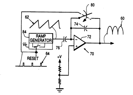
FIGURE 4 illustrates in block form a circuit for producing a
parabolic correction signal according to an aspect of the invention.
5 The sawtooth shaped output signal 62 of a periodically reset ramp
generator 84 is AC coupled to an active integrator 70 via a series
capacitor 76. The integrator 70 comprises an operational amplifier
72 and a feedback capacitor 74, and produces the parabolic output 60
as shown.
The ramp generator 84 can comprise a constant current supply
for charging a capacitor, producing an ascending ramp voltage, and
first resetting means 86, such as a transistor switch, for quickly
discharging the capacitor to cause the voltage to drop off at the
conclusion of the vertical or horizontal interval. Integration of the
15 AC coupled ramp signal produces a repetitive parabola signal, useful
for correction of pincushion distortion. However, the parabola
signal produced by the integrator 70 is subject to variation due to
periodic and/or transient variations which occur in the ramp signal
62. These periodic or transient variations can result, for example,
20 from vertical rate disturbances coupled from the vertical deflection
system and from loss of vertical sync during channel change. In
either case, the timing disturbances are coupled through capacitor
76, which has a long time constant to prevent distortion of the ramp
signal. The timing errors change the average voltage level at the
25 input to the integrator 70. The difference in average voltage level is
processed by the integrator as a DC offset, which distorts the
steady state shape of the parabolas. In view of the long time
constant of the integrator, the average voltage error will require
several vertical periods to dissipate. If the timing disturbance is
30 periodic and repetitive, the average voltage level error in the
integrator will not have an opportunity to dissipate. Instead, the
error will accumulate, increasing the distortion of the parabola.
According to an aspect of the invention, the capacitor 74 forming
the feedback path of the operational amplifier 72 of integrator 70 is
35 coupled to an auxiliary resetting means 80, such as a transistor
switch, operative to discharge the capacitor 74 during the
-
20397~5
-1 O-
occurrence of reset pulse 64. This periodic initialization prevents
any accumulation of error, and assures that each parabola generated
will start with a zero average voltage level, that is, with no
unintended DC offset. Such a circuit in accordance with aspects of
5 the invention is substantially insensitive to variations in the ramp
signal 62.
Different forms of periodic and/or transient variations can
affect the generation of the ramp signal and therefore the parabola.
Certain disturbances, for example, characterized as phase distortion
o or timing distortion, or both, resulting from operation of the
vertical deflection circuit can alter the constancy of the width and
frequency of the horizontal retrace pulses. Timing disturbances at a
vertical rate and multiples thereof can be coupled through the
secondary windings of the integrated high voltage transformer. The
15 timing disturbances can modulate the horizontal retrace pulses, by
altering pulse width or frequency, or both. The horizontal retrace
pulses are used to reset the ramp generating portion of the parabola
generator at the horizontal rate. Some vertical deflection systems,
for example switched mode vertical deflection systems, can produce
20 significant phase distortion in all the secondary windings of the
integrated high voltage transformer due to the switched mode of
operation. The phase distortion can be most pronounced during the
last part of vertical retrace, when the current through the switched
elements, for example an SCR for effecting switched vertical
25 retrace, is at its peak. The loading from this current modulates the
horizontal retrace pulses, causing variation of pulse width or
variation of frequency, or both, even from line to line. As a result,
the ramp signal in a parabola generator, for example, will not have a
constant frequency, and the ramps will have different maximum
30 amplitudes. Horizontal rate ramp signals can be integrated to
produce a horizontal rate parabola for North-South pincushion
correction, or used as a modulation signal for side pincushion
correction. Variations in the start time of the ramps, the duration
of the ramps and the maximum amplitude of the ramps will have a
35 detrimental effect on the parabolas or modulated signal envelopes.
As a result of the variations in the horizontal retrace pulses, the
203~77S
horizontal rate parabola signal and/or modulation signal can vary in
amplitude at the vertical rate.
Another problem having a similar detrimental result on
correction waveforms can occur during a channel change, when the
5 vertical deflection circuit must lock to the synchronizing signals of
a new video signal. Locking onto a new video signal can not be
accomplished instantaneously, but requires a certain time interval.
The loss of vertical synchronizing pulses during channel change will
consequently result in the loss of vertical reset pulses and vertical
10 retrace pulses. In order to prevent the raster from collapsing, most
vertical deflection circuits provide for a free running mode at a
slightly slower frequency than the vertical rate. When changing
channels, the vertical deflection ramp charges longer than normal
until a valid sync signal from the new video signal is detected,
15 because the vertical period is effectively increased by the lower
free running frequency. The effect of the extended charging of the
vertical ramp is that the average value of the ramp signal AC
coupled to the integrator will increase considerably, so that the
shape and size of the parabolas generated after restoration of
20 vertical sync will reflect a substantial DC offset voltage. The
offset voltage can require several vertical fields to return to a zero
average value. During this time, the pincushion correction circuits
can deviate substantially from their steady state levels. The
resulting error, in a projection television having superimposed
25 rasters and composite correction waveforms driving the auxiliary
deflection coils, is referred to as convergence bounce following a
channel change. The problem can be overcome according to another
aspect of the invention by also resetting the integrator at the
vertical rate, for example by the same vertical retrace pulses used
30 to reset the vertical rate ramp generator. This assures that the
integrator will be initialized after each vertical trace so as to begin
each successive vertical trace with no DC offset voltage.
In each of the foregoing examples, the integrator of a parabola
generator, as well as the ramp circuit, are reset by the reset pulse.
35 The auxiliary reset function of the parabola signal dependably
initializes, that is zeroes, the integrator before the beginning of
203977~
~_ -1 2-
each repetitive parabola. This eliminates undesirable periodic
variation of the parabola signal from timing disturbances
originating in vertical deflection systems and prevents distortion of
the parabolas following restoration of vertical sync, for example
5 after channel change. In prior art systems, each repetitive parabola
begins from whatever residual DC offset is processed by the
integrator, as a result of a distorted ramp signal. Such circuits are
subject to considerable distortion, particularly during channel
change when vertical sync is temporarily lost and particularly when
10 used in conjunction with noisy vertical deflection systems, such as
those operating in a switched mode. According to an aspect of the
invention, each repetitive parabola is always initialized from a
predefined level, for example a zero DC offset, due to an auxiliary
reset function responsive to a timing signal.
FIGURE 5 illustrates a circuit schematic for implementing a
correction circuit for North-South pincushion distortion, according
to an aspect of the invention. The circuit comprises a ramp
generator having a current source in the form of PNP transistor Q1,
whose collector is coupled to integrating capacitor C2. Current
source transistor Q1 charges capacitor C2 to form the ramp or
sawtooth signal at the horizontal scanning rate. The emitter of Q2
is coupled to the positive supply through resistor R3. The level at
the base of Q1 is fixed by a voltage divider comprising resistors R1
and R2. A capacitor C1 decouples the voltage divider junction (and
the base of Q2) relative to the positive supply. Subject to feedback
to the emitter of Q1 via R16 and C8 as discussed hereinafter, the
current supplied by current source Q1 is substantially constant,
whereby integrating capacitor C2 charges constantly to obtain a
ramp.
Integrating capacitor C2 is discharged by switching transistor
Q2 during the horizontal retrace. Resistors R4 and R5 couple the
base of transistor Q2 to a reset signal from the horizontal
deflection circuit 106, for example to the secondary winding of the
IHVT that produces retrace pulses. Diode D1 clamps the base of Q2
with respect to ground. During a retrace pulse, capacitor C2 is
discharged and upon completion of the retrace pulse C2 begins to
2039~77S
-1 3-
charge again, the signal at C2 therefore defining a sawtooth at the
horizontal rate.
The sawtooth is coupled to a follower amplifier stage formed
by PNP transistor Q3, whose emitter is coupled to the positive
supply through resistor R6, and reproduces the sawtooth. The
sawtooth is AC coupled through series capacitor C3 and resistor R7
to an active integrator. The integrator comprises operational
amplifier U1, to which the ramp signal is coupled at the inverting
input. Feedback capacitor C4 is coupled between the output of the
operational amplifier and the inverting input. Resistors R9 and R10
are coupled to the positive and negative 12V power supplies,
respectively. By integrating the AC coupled horizontal rate ramp
signal, a parabola 60 at the horizontal rate is obtained at the output
of operational amplifier U1. A vertical deflection circuit 90
provides an output to a vertical sawtooth circuit 92, which in turn
generates a vertical sawtooth signal as an input for a North-South
pincushion correction circuit 94. The vertical deflection circuit can
be a switched mode vertical deflection circuit. Switched mode
vertical deflection circuits are known in the art and need not be
described herein in detail. Mention can be made that switched mode
vertical deflection circuits comprise active switching elements, for
example SCRs. The switching elements can conduct large scanning
currents, particularly near and during vertical retrace. The
switching elements can be a source of considerable noise, at
vertical scanning rates and multiples thereof, which can easily
couple to other circuits, for example through the high voltage or
flyback transformer. The North-South pincushion correction circuit
modulates the parabola by the vertical sawtooth signal, at the
vertical rate, in a known manner. The modulated signal is coupled to
a summing circuit 100. Other inputs to summing circuit 100 are
generated by trapezoid correction circuit 96 and convergence
correction circuit 98. A composite correction signal is coupled to
output amplifier U2, for driving the auxiliary vertical deflection
yoke Y1.
The repetitive parabola signal developed at the output of
operational amplifier U1 can be somewhat advanced in phase
203977S
-1 4-
relative to generation of the raster, due to signal processing
elsewhere in the television circuitry. Under these circumstances, it
might be necessary to insert a phase delay, for example after the
output of the operational amplifier, to compensate for the phase
5 difference. Instead, resistor R8 adds a DC bias to the ramp signal,
which raises the ramp signal level relative to a zero voltage level
baseline. This has the effect of shifting the center of the parabola,
as though the parabola had been delayed in time. The DC bias does
alter the shape of the parabola to a small extent, but not enough to
10 disturb the convergence correction.
According to the invention, switching means are provided to
discharge the feedback capacitor C4. Discharging C4 turns the
integrator configuration of the operational amplifier into that of a
follower amplifier, setting the output to the level at the
15 noninverting input, which is grounded. Accordingly, the parabola is
initialized to zero amplitude as of a point in time defined by the
retrace pulse rather than reaching its minimum as a function of the
integration of the ramp and the time constant constrained discharge
of the capacitor. This removes any error which may accumulate due
20 to the fact that the ramp generation is coupled at least indirectly to
the switched vertical deflection circuit through the integrated high
voltage transformer (IHVT), and may be modulated thereby at the
vertical rate.
The switching means for discharging capacitor C4 includes
25 switching transistor Q5, coupled in parallel with capacitor C4 and in
series with resistor R18 at its emitter. The base of transistor Q5 is
coupled to the retrace pulses from horizontal deflection circuit 106
through a differentiator formed by capacitor C9 and resistor R17.
Differentiating the pulses produces a high going pulse at the leading
30 edge and a low going pulse at the trailing edge of the retrace pulse.
The low-going pulse is cancelled by diode D2, clamping the base of
transistor Q5 relative to ground. The differentiator produces a very
narrow pulse, whereby capacitor C4 is quickly discharged coincident
with the leading edge of the retrace pulse. Resistor R32 is series
35 coupled in the retrace signal path to capacitor C9, and provides
protection against arcing of the kinescope (not shown).
-15- 2039775
According to the embodiment of FIGURE 5, the parabola
obtained at the output of operation amplifier U1 is fed back to the
current supply transistor Q1 to modulate the otherwise constant
current supply and give the ramp at integrating capacitor C2 the
modified shape shown in FIGURE 5. The parabola is AC coupled via
capacitor C6 and series resistor R11 to an inverting amplifier stage
including transistor Q4. The base of transistor Q4 is biased by
resistors R12 and R13. Resistors R14 and R15 set the gain for
transistor Q4. The inverted signal is AC coupled via series resistor
R16 and capacitor C8 to the collector of current supply transistor Q1.
The added current to Q1 during the times in the cycle when the
parabolic output signal at the output of U1 is at is minimum causes
the charging rate of capacitor C2 to be greater at the beginning and
end of the ramp. The result is a modified parabola shape wherein the
slope of the parabola is greater at the lateral sides, which reduces
residual gullwing distortion in the raster. This aspect of the circuit is
explained in more detail in commonly owned, copending application
serial no. 2039780-2, laid open 28 October 1991, entitled Pincushion
Correction Circuit With Gullwing Compensation, by E. Rodriguez-
Cavazos, et al.
The circuit schematic shown in FIGURE 6 is arranged for
correction of East-West pincushion distortion rather than North-
South. Accordingly, a sawtooth is produced at the vertical rate and
is integrated to form a parabola which is modulated at the horizontal
rate, correcting lateral distortion as shown in FIGURE 3. Circuits for
correction of both forms of distortion are preferably included in the
television apparatus. In FIGURE 6, PNP current supply transistor
Q6 supplies a constant current to charge integrating capacitor C10.
As in the foregoing embodiment, a voltage divider including R19
and R20 sets the level at the base of Q6, which is decoupled
relative to the positive supply by capacitor C9. Transistor Q6
maintains a constant current though R21, coupled to the positive
supply, thereby producing a ramp at integrating capacitor C10.
Capacitor C10 is discharged at the vertical rate by a switching
means coupled to vertical retrace triggering means in vertical
deflection circuit 90. In the represented embodiment, the switching
means includes transistor Q7, coupled to the integrating
''`X
!
203977~
-1 6-
capacitor C10 through resistor R35. The base of transistor Q7 is
coupled to the vertical deflection circuit 90 via series and parallel
resistors R22 and R23, respectively, which set the appropriate level.
The ramp at the vertical rate obtained at integrating capacitor
5 C10 is coupled to a follower amplifier comprising PNP transistor
Q8, whose emitter is coupled to the positive supply through resistor
R24 and whose collector is grounded.. Inasmuch as the ramp at C10
in this embodiment is linear, rather than modified as in FIGURE 5,
the vertical sawtooth signal at the emitter of transistor Q8 can be
10 used in other circuits. For this purpose, the emitter of Q8 is coupled
to an NPN transistor Q11 via series capacitor C15. The base of
transistor Q11 is biased by resistors R33 and R34.
The emitter of Q8 of the follower amplifier stage is AC
coupled through series capacitor C11 and resistor R25 to the
15 inverting input of operational amplifier U3. A feedback path
including capacitor C12 couples the operational amplifier inverting
input and output, to form an active integrator. Leakage resistor R26
is coupled in parallel to C12, as is switching transistor Q10.
Transistor Q10 discharges capacitor C12 at the beginning of a
20 vertical retrace pulse. Inasmuch as the noninverting input to
operational amplifier U3 is set at a fixed positive voltage by a
voltage divider including resistors R27 and R28, the output of U3 is
set to this voltage when transistor Q10 discharges capacitor C12.
The vertical retrace pulses are differentiated by capacitor C13 and
25 resistor R31, forming a narrow pulse at the beginning of the vertical
retrace pulse. The differentiated output is clamped relative to
ground by diode D3. As C10 is periodically charged and reset at the
vertical rate, the ramp or sawtooth thereby produced is integrated
to form a parabola at this rate at the output of operational amplifier
30 U3.
The parabola at the output of U3 is AC coupled by series
capacitor C14 to a further amplifier stage including transistor Q9.
The base of transistor Q9 is biased by resistors R29 and R30. The
vertical rate parabola is an output at the emitter of transistor Q9.
35 The emitter is coupled to horizontal pincushion correction circuit
106, where the vertical rate parabola is modulated by a horizontal
203977S
-1 7-
rate sawtooth. The horizontal pincushion correction circuit 110
receives a horizontal sawtooth signal from horizontal sawtooth
circuit 108. Horizontal sawtooth circuit 108 is responsive to
horizontal deflection circuit 106. The output of horizontal
5 pincushion correction circuit 1 10 is a summing circuit 102. Other
inputs to the summing circuit 102 are generated by the trapezoid
correction circuit 96 and the convergence correction circuit 98. The
output of summing circuit 102 is coupled to amplifier U4 for driving
the auxiliary horizontal deflection yoke X1.
In each of the foregoing embodiments, the feedback capacitor
of an active integrator in a parabola generator is positively
discharged by switch means at a point in time defined by a timing
pulse, for example at the leading edge of a retrace pulse. In the
embodiment of FIGURE 5, the auxiliary reset function prevents
15 distortion of the horizontal correction parabola by vertical rate
phase and timing disturbances, for example those caused by
switched mode operation of a vertical deflection system. In the
embodiment of FIGURE 6, the auxiliary reset function prevents
distortion of the vertical correction parabola by vertical rate phase
20 and timing disturbances, for example those caused by switched mode
operation of a vertical deflection system, particularly at the time of
vertical retrace. However, there is a further advantage.in the
embodiment of FIGURE 6. Normally, vertical retrace triggering is
derived from the received video signal. During a channel change,
25 when vertical sync is lost, a free running circuit in the vertical
deflection circuit will provide internal vertical synchronizing
pulses to prevent the raster from collapsing, although at a lower
frequency than the vertical rate. Inasmuch as the vertical ramp is
reset by the vertical retrace signal, the vertical ramp charges
30 longer during the transient period following a channel change
because the internal vertical period is longer, until a valid
synchronizing signal is detected for the new channel. The auxiliary
reset function prevents the longer charging of the vertical ramp
during channel change from effecting the steady state values of the
35 vertical rate parabolas generated after vertical sync is
reestablished, so as to prevent convergence bounce.
203~77~
-1 8-
Generally, the time constants throughout the correction
circuits produce unacceptable performance if the horizontal and
vertical rate parabolas deviate from their respective steady state
levels. The auxiliary reset function in the integrator, responsive to
5 a timing signal according to aspects of the invention, enables the
steady state levels to be more closely maintained.