Note: Descriptions are shown in the official language in which they were submitted.
2040026
1 TITLE OF THE INVENTION
INPUT MATCHING CIRCUIT
BACKGROUND OF THE INVENTION
(Field o~ the Invention)
The present invention related to an input matching
circuit connected to an input circuit o~ a low noise
ampli~ier which is used in a converter ~or direct
broadcast satellite (DBS) systems.
(Related Background Art)
A noise ~igure (NF) of an ampli~ier which uses a
field e~ect transistor (FET) varies with a signal
source impedance viewed from the FET toward a signal
source, and it is minimum at certain signal source
impedance (Zopt) Thus, an input matching circuit is
provided in the signal source o~ FET so that the signal
source impedance viewed ~rom the FET assumes an optimum
signal source impedance Zopt
However, the optimum signal source impedance Zopt
varies with variation in the manu~acture of the FET. A
prior art input matching circuit of the low noise
amplifier has been designed such that the signal source
impedance viewed ~rom the FET is a mean value o~ the
variations o~ the optimum signal source impedance Zopt
However, a constant noise contour on a Smith chart
for FET 1 is not symmetric to the optimum signal source
impedance Zopt but it is of~set. As a result, even i~
an external impedance (~on ) is converted to the
~r
20~0026
meanvalue Or the optimum signal source impedance Zopt~ a
meanvalue oi variations oi the NF oi the ampliiier is
not necessarily minimum due to the oiiset oi the
constant noise contour.
SUMMARY OF THE INVENTION
It is an object oi the invention to resolve the
above problem. In accordance with the present
invention, the input matching circuit adapted to be
connected to an input circuit of an ampliiier is
characterized by that a line connecting a point on a
Smith chart indicating a mean value of variations oi an
optimum signal source impedance due to manuiacture
variations of the amplifier and a center point oi the
Smith chart is drawn, two points on the line which are
spaced from the mean value point by predetermined
multiples oi a standard deviation oi variations oi said
optimum signal source impedance are determined, a
crosspoint oi those constant noise contours in two
groups oi constant noise contours respectively having
the two points as the optimum signal source impedances
and imparting the same noise iigure on the line is
determined, and the signal source impedance as viewed
from said low noise ampliiier is designed to have the
impedance indicated by said crosspoint. The matching
point thus determined is located such that an interval
between the constant noise contour is larger than that
2040026
1 where the meanvalue Or the variations oi the optimum
signal source impedance of the ampliiier to be connected
is used as the matching point. Accordingly, even if the
optimum signal source impedance varies, the change Or
the noise index is gentle and the mean value of the
manufacturing variations o~ the NF of the low noise
amplifier is smaller.
The present invention will become more fully
understood from the detailed description given
hereinbelow and the accompanying drawings which are
given by way of illustration only, and thus are not to
be considered as limiting the present invention.
Further scope of applicability of the present
invention will become apparent from the detailed
description given hereinafter. However, it should be
understood that the detailed description and specific
examples, while indicating preferred embodiments of the
invention, are given by way of illustration only, since
various changes and modifications within the spirit and
scope of the invention will become apparent to those
skilled in the art from this detailed description.
BRIEF DESCRIPTION OF THE DRAWINGS
Fig.l shows a Smith chart for illustrating setting
of a matching point in a low noise amplifier in one
embodiment of the present invention,
Fig.2 shows a smith chart for illustrating a locus
2040026
1 oi constant noise rigureæ,
Fig.3 shows a Smith chart ~or explaining magnitude
o~ interval o~ constant noise contours,
Fig.4 shows a Smith chart ~or explaining a
di~erence between variations o~ noise indices due to
di~erence in positions o~ matching points ~or impedance
conversion, -
Fig.5 shows a con~iguration o~ a ampli~ier o~ theembodiment,
Fig.6 shows a Smith chart ior explaining a shi~t
status o~ matching point in the ampli~ier shown in Fig.
6, and
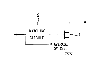
Fig. 7 shows a prior art amplifier.
DETAILED DESCRIPTION OF THE PREFERRED EMBODIMENTS
In general, the NF (herein a~ter F) o~ the FET is
represented by
F= Fmin + (4Rnlrs ~ roptl )
/ {(l-lrsl2)ll + rOptl2}
where Fmin is a minimum value o~ NF,
Rn is equivalent noise resistance
Fs is a signal source power reflection coe~ficient
ropt is optimum signal source power reflection
coe~icient which minimizes NF
ropt and Zopt have a relationship o~
Zopt ~ 50
ropt
Zopt + 50
ropt and Zopt indicate the same point on a Smith chart.
20~0026
There are inrinite number o~ combinations oi signal
source power re~lection coei~icient rs in which F
(excluding Fmin) assumes a constant value, and a locus
thereo~ is a circle on a smith chart shown in Fig.2.
This circle is called a constant noise contour, and a
center (CFi and a radius RFi oi the constant noise
contour ~or a noise index Fi are given by
CFi = ropt / ( 1 + Ni )
RFi = { 1 / ( 1 + Ni ) } {Ni2 + Ni ( 1 - ¦ ropt ¦ ) }
Where Ni={(Fi-Fmin)/4Rn} 11 ropt
As seen ~rom the above equation, the center CFi o~
the constant noise contour is on the vector rOpt
and the respective circles are not concentric. As a
result, the interval of the constant noise contour is
smallest toward the vector rOpt starting ~rom rOpt, and
largest toward the vector -rOpt . The mean value o~
variations of rOpt is represented by MtrOpt]as shown in
Fig.3. The variation when rOpt changes toward the
vector M[ropt] relative to M[ropt] and the variation
when rOpt changes toward the vector -M[ropt] are equal
in the distance, but the change in the NF is largest
when rOpt changes toward the vector M[ropt] because the
interval of the constant noise contours increases to the
largest along the vector M[ropt]~ On the other hand,
when rOpt changes toward the vector -M[ropt]~ the
interval of the constant noise contours changes to the
smallest along the vector so that the change in the NF
2040026
is small, which is a desirsble condition.
Accordingly, ii the input matching circuit is
matched not to M[ropt] but to a point slightly shiited
irom M[ropt] toward the vector -M[ropt]~ the mean value
oi the manuiacture variations oi the NF oi the low noise
ampliiier can be reduced. For example, it is assumed
that the input matching circuit is matched to a point rQ
shown in Fig.4. M+[ropt] represents a point assumed
when rOpt is shiited irom M[ropt] by a predetermined
amount toward the vector M[ropt]~ and M ~rOpt]
represents a point assumed when rOpt is shiited irom
M[ropt] by the same amount toward the vector -M[ropt]~
Three constant noise contours are drawn ior each oi the
points M+[ropt] and M [rOpt]. The circles correspond to
Fmin+ldB~ Fmin+2dB and Fmin+3dB-
Ii the input matching circuit oi the ampliiier isdesigned to match to M[ropt]~ the NF oi the ampliiier is
deteriorated by ldB when rOpt is shiited to M+[ropt]~
and deteriorated by 3dB when rOpt is shi~ted to
M [rOpt]. The amounts oi shiit oi rOpt in the
respective directions are equal and represented by
IM+[rOPt]-M[rOPt] I = IM [rOPt] M[rPt] I
However, although the amounts oi shi~t are equal,
the degree oi deterioration oi the NF diiiers depending
on the direction oi shiit oi rOpt.
On the other hand, ii the input matching circuit oi
the ampliiier is designed to match to the point rQ shown
- 204002S
in Fig.3, the NF o~ the ampliiier is Fmin + 1.5dB when
ropt ~ the FET is shi~ted to either M+[ropt] or
M~[rOpt],and the meanvalue o~ the manu~acture variations
o~ the NF o~ the ampli~ier is reduced. A statistical
property of the manu~acture variations o~ rOpt greatly
depends on a device structure, a device size and a
manu~acturing process and an optimum value oi rQ cannot
be generally de~ined.
However, as ~or the constant noise contour when
rOpt = M+[Popt] and the constant noise contours when
ropt = M-[ropt]~ there is one NF value at which the
constant noise contours which impart the same NF value
cross a line connecting Mtropt] and a center o~ a Smith
chart. In the above example, that value is Fmin +
1.5dB. Thus it is optimum to set rQ around the
crosspoint in order to minimize the mean value o~ the
variations of the NF. However, to determine the ranges
of M+[ropt~ and M [rOpt] relative to the variations o~
rOpt, statistical data o~ the manu~acture variations o~
rOpt is necessary. In general, it may be set to +a- +3a
(when a is a standard deviation of manufacture
variations o~ rOpt).
The above discussion is explained by speci~ic
examples.
It is assumed that the mean value M[ropt] oi the
manu~acture variations o~ rOpt is (0.7, 100'),
that is,
20~002~
1 IMtropt]l=0-7
angle Mtropt]=loo
and the standard deviation ~ ¦ropt¦ is 0.05.
¦Mtropt]l represents the mean value o~ variations o~ the
absolute value o~ rOpt, and angle Mtropt] represents the
mean value o~ variations o~ phase angle o~ rOpt. In
accordance with the above discussion, M+tropt] and M
trOpt] are set as iollows.
M+tropt]=(o.8~ 100 )
M-[rPt]=(0.6, 100')
The distances ~rom M+[ropt] and M-[ropt] to M[ropt]
are +20. Then, the constant noise contours are drawn
~or ropt=M+[rOpt] and ropt=M~[rPt]
I~ the circle RF+ ~or Fmin + a(dB) o~ the constant noise
contours for ropt=M+[ropt]~ and the circle RF- ~or Fmin
+ a(dB) o~ the constant noise contours ~or rOpt = M
[rOpt] cross on the line connecting M[ropt] and the
center oi the Smith chart shown in Fig.1, the crosspoint
may be used as rQ in designing the input matching
circuit oi the ampli~ier. Namely, the input matching
- circuit is designed to convert the impedance from ~OQ to
rQ.
Such an input matching circuit is shown in Fig.5,
- which may be implemented by an open stub A and a
- microstrip line B. This is explained with re~erence to
an imittance chart shown in Fig.6. Both the open stub
A and the microstrip line B are ~ormed by microstrip
20~0026
1 lines having a characteristic impedance o~ 50n. The 50n
point at the center Or the Smith chart is converted to a
point P by the open stub A. Since a suceptance o~ the
point P is j-1.7, an electrical length Q11 ~ the open
stub A may be set to
Q11=tan-11.7=59 5.
An electrical length Q12 of the microstrip line B may
be set to convert the point P to rQ. A wavelength for
the point P is 0.069 when it is read ~rom a wavelength
circle on an extended line o~ a line OP, where 0 is the
center of the chart. Similarly, a wavelength ~or rQ is
0.111. Accordingly, the electrical length Q12 ~ the
microstrip line B is given by
Q12=360 x (0.111+0.069)=64.8'
Accordingly, the open stub A in the input matching
circuit may be designed to have the characteristic
impedance o~ 50n and the electrical length Q11 f 59 5'~
and the microstrip line B may be designed to have the
characteristic impedance o~ 50Q and the electrical
length Q12 of 64-8 -
In the past, when the input matching circuit is
designed, it is designed such that the input matching
circuit matches to the mean value o~ the manufacture
variations o~ rOpt. Namely, the input matching circuit
is matched to Mtropt] on the smith chart o~ Fig.4.
However, since the constant noise contours are not
concentric as described above, such design does not
2040026
-
1 necessarily minimize the mean value oi the variations o~
the NF oi the amplirier caused by the variations o~
rOpt, because the intervals oi the constant noise
contours are not uni~orm. In the low noise ampli~ier
which uses the input matching circuit of the present
invention, the matching point is shi~ted toward larger
interval oi the constant noise contours so that the mean
value of variations o~ the NF o~ the ampli~ier caused by
the variations o~ rOpt is minimized.
From the invention thus described, it will be
obvious that the invention may be varied in many ways.
Such variations are not to be regarded as a departure
from the spirit and scope o~ the invention, and all such
modi~ications as would be obvious to one skilled in the
art are intended to be included within the scope o~ the
following claims.