Note: Descriptions are shown in the official language in which they were submitted.
204026 ~
DISABLING ARRANGEMENT FOR A CII~CUIT
OPERATING AT A DEFLECTION RATE
The present invention is related to a video display
apparatus. In particular, the present invention is directed to a
circuit for actively disabling, for example, a pulse-width-
modulator and a pincushion distortion correction circuit in a
television receiver in order to prevent ringing signals from
producing damage to circuit components.
It is known to provide a television receiver which is
capable of operating in a standby mode and in a power-on, run or
normal mode. In the normal mode, the television receiver
operates to process video and audio signals and to display those
signals. In a standby mode the deflection stages are disabled.
However, a microprocessor of a remote control circuit is powered
and set for operation but the receiver does not process or display
video or audio signals.
A switch mode power supply primary circuit may
regulate output supply voltages by sensing corresponding voltages
produced at either the primary side of an isolation chopper
2 0 transformer that is referenced to a "hot" ground or at a secondary
side of the chopper transformer that is referenced to a "cold"
ground, depending upon the mode of operation selected by the
user. The primary circuit is a regulator circuit portion that is at
the primary side.
2 5 The selection of either the standby mode or the
normal mode is indicated to the switch mode power supply
primary circuit by the presence of an output signal of a pulse
width modulator which is at the secondary side and which is
coupled to an input of the switch mode power supply primary
circuit. The output of the pulse width modulator in the normal
mode are pulses at the horizontal line rate with a duty cycle that
is variable depending on the condition. When pulses are received
at the primary circuit, this indicates to the primary circuit that a
normal mode of operation is required. The primary circuit
3 5 produces an output signal, which is in part dependent upon the
pulses received from the pulse width modulator. The output
signal controls a chopper transistor of a chopper circuit that is
coupled to the chopper transformer. Voltages produced at
secondary windings of the transformer are rectified to produce
*
2 2040261.
-
supply voltages that are referenced to the cold ground. The
magnitude of a given supply voltage is dependent upon the pulse
width of the pulses received at the input of the primary circuit.
The primary circuit also includes an over current detector for
detecting an over current condition in the chopper transistor.
In the standby mode, the pulse width modulated
signal is disabled. The primary circuit detects the absence of the
modulated signal and then regulates off the primary side of the
transformer that is referenced to "hot" ground, in the standby
1 0 mode .
The output supply voltages are utilized to supply
power to various low voltage loads in the receiver. A supply
voltage B+ of the output supply voltage provides power to a
horizontal output circuitry. The output supply voltages are
produced in both the standby and normal modes
A typical horizontal deflection output stage of a
television receiver, for example, includes a flyback transformer.
A primary winding of the flyback transformer is coupled to a
deflection switch responsive to a horizontal rate control signal that
is obtained from a horizontal oscillator and driver stage. The
switch operates at the horizontal frequency in normal mode. A
deflection winding forms with a capacitor or resonant circuit that
is also coupled to the deflection switch.
During normal mode of operation, the deflection switch
2 5 produces switching operation and develops a voltage at the
horizontal frequency across the primary winding. A retrace
voltage at the horizontal frequency is also developed in a
secondary winding of the flyback transformer by a transformer
action.
3 0 The horizontal rate voltage at the secondary winding,
hereinafter referred to as the switching signal, may be used for
providing switching operation at the horizontal rate. The
switching operation is provided in various circuits, for example, in
the pulse-width-modulator of the power supply and in an East-
3 5 West pincushion distortion correction circuit.
Standby mode of operation is accomplished by
disabling the horizontal oscillator when an on/off signal at an OFF
state is provided by the remote control circuit. The horizontal
3 204026 1;
_
oscillator generates, in normal mode, a horizontal rate control
signal that produces switching in the deflection switch.
Immediately after the horizontal oscillator is disabled, deflection
energy is still stored in capacitors and inductances of the
5 deflection circuit output stage such as at the deflection winding.
Therefore, during an interval that may last a few milliseconds
following the instant when the horizontal oscillator is disabled,
ringing at a frequency of, for example, 3 KHZ having a gradually
diminishing amplitude can be produced in the aforementioned
10 switching signal that is developed at the secondary winding of the
flyback transformer. This switching signal is fed to the pulse
width modulator (PWM) which supplies a regulator control input
signal to the switch mode regulator primary circuit, as explained
before. It is also fed to the switch mode pincushion distortion
15 correction circuit. If the ringing in the switching signal were
permitted to affect the pulse width modulator, the modulator
would have produced wide pulses at a low frequency as a result
of the ringing, that are substantially wider and at a lower
frequency than in normal mode. The pulse width modulator
2 0 provides such pulse signals to the switch mode power supply
primary circuit which in turn controls the chopper transistor by
way of the output signal, as explained before. An abnormally
large current might have been produced in the chopper transistor
because of the abnormally wide pulses. This, disadvantageously
2 5 could trip an over current shut down protection circuit, thereby
disabling the power supply and removing the power from the
remote control receiver.
As described above, the presence or absence of pulses
at an input of the primary circuit is the determining factor to that
3 0 primary circuit as to selecting the operational mode. Therefore,
disadvantageously, the ringing could cause the primary circuit not
to change states to operate at the standby mode and could over
time, due to large currents in the chopper transistor, damage that
transistor and/or adversely affect the microprocessor because of a
3 5 supply voltage drop.
Furthermore, since the switching signal developed at
the secondary of the flyback transformer is also used for
controlling the pulse width modulator of a switch mode
2Q~0261
4 RCA 86,029
_
pincushion circuit, wide pulses caused by the ringing could have
produced wide current pulses in a transistor associated with the
pincushion circuit. Such current pulses might have damaged that
pincushion circuit output transistor unless more expensive
S transistor were used having power tolerance prescribed at a high
enough level.
In accordance with an aspect of the present invention,
an active turnoff circuit disables the output ringing related pulses
produced by a pulse width modulator after a transition to the
standby mode. In addition, an active turnoff circuit is provided so
as to cut off or prevent the ringing in the switching signal from
causing a damage to the pulse width modulator output transistor
associated with e.g., the pincushion circuit.
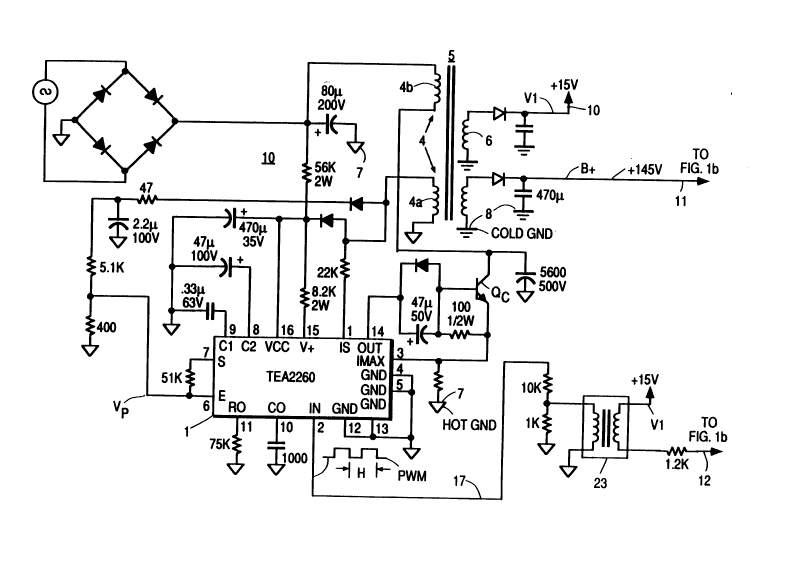
FIGURE la illustrates the power supply portion of a
television receiver circuit to be utilized together with circuitry
according to the present invention.
FIGURE lb illustrates a second portion of a receiver
circuit including an embodiment of the present invention which
circuit is coupled to the circuit of FIGURE la.
FIG. la illustrates a first portion of a television
receiver circuit. A power supply primary circuit 10, operating as
a switch mode regulator control stage, includes a type TEA 2260
integrated circuit 1 which has a plurality of terminals or
connections. Connection 2 iS coupled via resistors to one side of an
isolation transformer 23 that is referenced to "hot" ground 7. The
other side of the transformer has its windings coupled to a 15 volt
supply voltage Vl that is referenced to a "cold" ground 8 and also,
via a resistor to a second portion of the receiver circuit which is
illustrated in FIG. 1 b and which includes a pulse width modulator
3 0 circuit 31.
The primary circuit 10 operates to regulate or control
the supply voltage from either the primary or secondary side of a
main chopper transformer 5. The primary side is referenced to
hot ground 7 while the secondary is referenced to cold ground 8.
3 5 Such a circuit has a standby mode of operation and a power-on,
normal or run mode of operation. In the normal mode of
operation the primary circuit 10 regulates from a voltage that is
sensed at the secondary side. Output signals from a connection 14
RcA 862d~ o 2 !~1
control chopper transistor QC- When the receiver is in the standby
mode of operation, the primary circuit 10 regulates from a voltage
developed in a winding of the hot side 4 of the transformer 5 by
producing signals at connection 14, an output pin of the switch
mode regulator control circuit. One such available control circuit
is the TEA 2260 integrated circuit available from SGS Thomson.
This control circuit regulates a voltage supply that is referenced
either to the hot ground or to the cold ground depending upon the
input at pin 2. That is, the presence or absence of pulses from the
pulse width modulator 3 1 , which is a component of the second
portion of the receiver circuit illustrated in Figure 1 b, determines
whether the primary circuit operates in either the standby mode
of operation or the normal mode of operation. When no pulses are
received, then the primary circuit operates in the standby mode,
thereby regulating from the hot side of the main transformer 5.
However, when such pulses are present at the input pin 2, the
primary circuit will operate in the normal mode of operation
producing an output signal that controls the chopper transistor.
The output signal at terminal 14 has pulse ~,vidth that is related to
2 0 that of the pulses received at the input terminal 2 thereby
regulating from the cold side of the main transformer. Pin 3
detects the chopper transistor current and determines if that
current exceeds a m~ximum value. If it does, the primary circuit
goes into over current shutdown.
FIG. lb discloses a second portion of the television
receiver circuit which is coupled to the first portion of the circuit
illustrated in FIG. la. In particular, lines 10, 11 and 12 of FIG. la
are coupled to lines 20, 21 and 22 of FIG. lb respectively.
Furthermore, FIG. lb includes a remote control receiver 24 which
3 0 produces an ON signal or an OFF, standby signal depending upon
the mode of operation selected by the user. This control device
can include a microprocessor. When the ON signal is produced by
the controller indicating the normal mode of operation, the
horizontal oscillator and driver 25 begins to produce horizontal
3 5 line pulses to be coupled to a conventional deflection circuit 26.
Circuit 26 includes a horizontal deflection winding LY and a
switching transistor 26a. Circuit 26 produces horizontal line
pulses of a horizontal rate switching signal 66 upon line 27 by a
6 204026 1
flyback transformer 28 via a winding 30. The horizontal line rate
pulses of signal 66 are then provided to the pulse width
modulator 31 via an integrating network comprising a resistor
R10 and a capacitor C10. The pulse width modulator 31 outputs
5 pulse-width-modulated pulses to line 22 which are received as
inputs at line 12 of Figure la. These pulses are then transferred
via transformer 23 to line 17 coupled to pin 2 indicating to
primary circuit 10 that the normal mode of operation is required.
Pulse-width-modulator 31 operates to provide pulse
1 0 width modulated pulses to control the supply voltage regulation
by the switch mode regulator power supply shown in Fig. la.
If the 145V B+ supply that is referenced to the cold
ground begins to rise, the rise in voltage is coupled via a voltage
divider 50 to the base of transistor Q10, causing Q10 to conduct
1 5 less heavily. The collector of Q10 is coupled to the emitter of Qll,
to the base of which the integrated ramp signals from the
secondary 30 are supplied. The reduction in the conduction of
transistor Q10 reduces the emitter voltage of Ql l, causing
transistor Qll to turn ON or OFF at a lower base voltage, thereby
2 0 providing narrower positive going pulses at the Q 11 collector
across resistor 51. These, in turn, turn ON transistor Q12
accordingly, inverting the pulses at the output of the collector of
Q 12 which are supplied to coupling transformer 23. Integrated
circuit 1 uses the pulse width duty cycle of the pulses at
2 5 connection 2 to control the ON and OFF time of transistor QC to
bring the B+ supply voltage down by turning transistor QC ON for a
shorter time. The lower voltage +Vl supply will track the B+
supply and will also accordingly, be regulated.
If the B+ supply decreases, the reverse situation
3 0 occurs, with transistor Q10 conducting more, raising the emitter
levels of transistor Q 11, and changing the time period over which
transistor Ql l conducts. This pulse width modulated signal at the
collector of Qll is provided via Q12 and transformer 23 to circuit
1, causing chopper transistor QC to turn ON for a longer duration,
3 5 driving the supply voltage B+ upward. Voltage Vl, of course,
tracks the B+ level and also rises.
A vertical deflection circuit 222 is coupled to a
noninverting input of a comparator 110 of a pincushion distortion
7 204026 ~ -
correction circuit 999. Signal 66 is also coupled to comparator 110
via a series RC connection of Rl and Cl which are coupled to line
27. The voltage appearing at the noninverting input of the
comparator 11 0 is compared to a reference voltage VREF to
5 produce an output voltage Vllo, which is coupled to the base of
switching transistor QPC. The horizontal pulse signal on line 27,
signal 66, is coupled via AC coupling capacitor Cl and is integrated
in a ramp capacitor C2. This circuit configuration comprising of
comparator 11 0 and transistor QPC forms a switch mode East-West
10 pincushion correction circuit.
When a transition to standby mode occurs, horizontal
oscillator and driver 25 is disabled by an internal on/off switching
transistor Q4 that is coupled to remote control circuit 24. Energy
that is still stored in circuit 26 produces ringing in signal 66
15 during a few milliseconds that follow. The ringing signals are
developed upon line 27 to thereby provide pulses to the pulse
width modulator 31 as well as to the switch mode East-West
pincushion correction circuit 999
Assume, for explanation purposes, that the pulse
2 0 width modulator 31 were permitted to react to these ringing
signals. Therefore, modulator 31 could begin to provide spurious
pulse width modulated output signals at a frequency
corresponding to a low frequency of the ringing signals of signal
66. These spurious signals could be coupled to the chopper
25 transistor QC and QPC and might induce very high current pulses
in these transistors potentially damaging them. For example, the
peak current in such transistors might exceed lA.
Therefore, the present invention introduces active
turnoff switching capabilities which result in actively turning off
3 0 the pulse width modulator 31 so as to prevent the ringing signals
at a frequency such as 3 KHZ that is substantially lower than the
horizontal frequency, from generating pulses which would
otherwise ultimately be received by the primary circuit 1.
Furthermore the circuit also suppresses any effect of the ringing
3 5 signals on transistor QPC-
In the present invention, a transistor Q 1 is providedhaving its emitter grounded and its base coupled, via resistor R, to
the output of the remote control receiver circuit 24. As a result,
8 RCA 8~026
the ON/OFF state of transistor Q 1 is determined by the output of
the remote control receiver circuit 24. The collector of transistor
Ql is coupled to the base of transistor Q2 via resistor R2 and is
also coupled to the base of transistor Q3 via the resistor network
S of R3, R4 and R5. Resistor R3 provides the collector voltage for Ql.
When Ql is turned ON by the remote control receiver circuit 24
,which produces an ON signal to the base of Ql that is a voltage
sufficient to bias transistor Ql ON, transistor Ql is turned ON and
transistors Q2 and Q3 are cut OFF. Thus the path from collector to
1 0 emitter of each of these two transistors Q2 and Q3 is effectively
an open circuit having little or no impact on the circuits which are
connected to their respective collectors.
In particular, the collector of transistor Q3 is coupled
to the collector-emitter coupling of transistors Q10 and Ql l of the
1 5 pulse width modulator 31. The collector of transistor Q2 is
coupled to the noninverting input of the comparator 110 of the
pincushion correction circuit 999. In the normal mode of
operation therefore, transistors Q2 and Q3 have no effect on either
the pulse width modulator 31 or the comparator 110 of the switch
2 0 mode East-West pincushion correction circuit. Therefore, the
horizontal pulses appearing on line 27 are received by the ramp
generator constituted by the resistor-capacitor combination R10-
C10 to produce a ramp signal at the base of transistor Qll. This
ramp signal is used to produce a sequence of pulse width
2 5 modulated pulses, as previously described. The transistor
configuration of Q10, Qll and Q12 results in an output of a pulse
signal on line 22 to line 12 of Figure la. Furthermore, the
pincushion correction circuit operates as if Q2 did not exist in the
clrcultry.
3 0 However, when the remote control indicates that the
user has selected the standby mode of operation, transistors Q2
and Q3 become conductive. In particular, when the output of the
remote control goes to a low signal, indicative of the standby
mode, transistor Ql is cut off. When transistor Ql is cut off,
3 5 transistors Q3 and Q2 are turned ON. This actively turns off or
disables the PWM circuit 31 protecting transistor QC and causing
the switch mode regulation to regulate from the primary side and
2040261
9 RCA 86,029
also actively protects the switch mode East-West pincushion
transistor QPC-
With respect to the active disabling of the pulse widthmodulator, once Q3 iS turned ON, the collector-emitter coupling of
Q10 and Qll is pulled to ground thus preventing the ringing
signals received from line 27 which have been converted into
ramp pulses by ramp generator R10-C10, from being coupled to
terminal 2 of circuit 1 of primary circuit 10. This is done by
providing a current path from the collector of Q10 and the emitter
10 of Qll to ground through transistor Q3. When Q3 turns ON, the
emitter of transistor Q 11 approaches ground effectively turning it
OFF. Note that transistor Qll base is biased positively by resistor-
diode voltage divider comprising Rll, R12, R13 and Zener diode
D10, ensuring cut-off.
The effect of any ringing pulses on line 27 on the
voltage at the base of transistor QPC iS also eliminated by
establishing a path to ground for the positive terminal of the
comparator 110 through the collector and emitter of transistor Q2.
This prevents a ramp voltage that would have otherwise produced
2 0 by the ringing signals and the ramp generator resistor R1 and
capacitor C2 from developing at the positive input of the
comparator 110 which would be sufficient so as to generate wide
current pulses at the base of transistor QPC. Thus, the transistor of
this switch mode East-West pincushion correction circuit is
protected against extended exposure to high current and a
transistor having a lower power tolerance can be used as this
element.
The PWM is disabled from producing wide pulses
which would otherwise produce wide current pulses in the
chopper transistor QC- Therefore, the chopper transistor is also
protected against exposure to high current and a transistor having
a lower power tolerance can be used as this element.