Note: Descriptions are shown in the official language in which they were submitted.
20406~1
Title of the Invention
INFRAReD RAY SENSOR AND METHOD OF MANUFACTURING
THE SAME
Background of the Invention
The present invention relates to an infrared ray sensor
for measuring the temperature of an object whose
temperature is to be measured in a non-contact state and a
method of manufacturing such an infrared ray sensor,
Infrared ray sensors designed to form an infrared ray
deteting element (temperature sensing element) on a bridge
above a substrate are known. Such infrared ray sensors
exhibiting an improved sensitivity have been proposed in,
for example, Japanese Patent Laid-Open Nos. 178149/1982 and
277528/1987.
Infrared ray sensors designed to provide a plurality of
infrared ray detecting elements on bridge substrates have
also been proposed. In such infrared ray sensors, infrared
radiation is made incident on half of the plurality of
infrared ray detecting elements while it is not made
incident on the remaining half thereof, and the difference
in the two outputs is calculated. Consequently, adverse
effect of the disturbance can be eliminated, and
sensitivity can thus be improved.
Such conventional infrared ray sensors, having a
plurality of infrared ray detecting elements so that a
difference between the output of the infrared ray detecting
2~Q~3~
element to which infrared radiation is made incident and
that of the infrared ray detecting element to which no
infrared radiation is made incident can be produced, have
the following concrete configuration.
That is, two ceramic substrates each of which has an
infrared ray detecting element formed thereon are
accommodated in a hermetic package having a window through
which infrared radiation enters. One of the substrates is
connected to the distal ends of the terminal pins of the
hermetic package in a state in which the infrared ray
detecting element thereof faces the window so that infrared
radiation can enter the element. The other substrate is
connected to the distal ends of the terminal pins of the
hermetic package at a position separated from the window so
that no infrared radiation enters its infrared ray
detecting element. The difference in the output between the
two infrared ray detecting elements is calculated, by which
adverse effect of the disturbance can be eliminated.
In recent years, attempts have been made to manufacture
supersmall infrared ray sensors by utilizing the
semiconductor microfabrication technologies.
Photolithographic and etching technologies are used to form
very small bridge structures on each of which an infrared
ray detecting element is formed. In this sensor, the
bridges each of which has the infrared ray detecting element
formed thereon are formed on one surface of the sensor
2 0 ~
substrate, and infrared radiation is detected from the
difference in the output between the infrared ray detecting
element on which infrared radiation is made incident and
the infrared ray detecting element on which no infrared
radiation is made incident, as in the former infrared ray
sensor.
However, the above-described convent-ional infrared ray
sensors have the following drawbacks.
In the configuration of the type in which the
substrates are accommodated in the hermetic package,
connection of the individual substrates to the terminals of
the hermetic package makes manufacture of the sensor very
difficult in terms of workability and reproducibility of the
position of the elements.
Furthermore, one of the infrared ray detecting elements
must be disposed at the position where it does not face the
window of the hermetic package in a state where it is
separated from the package case through a predetermined
distance. Also, it is difficult to maintain the positional
relation between the two infrared ray detecting elements in
an adequate state. This causes a slight amount of infrared
radiation to be made incident on the infrared ray detecting
element to which no infrared radiation is to be made
incident. The amout of infrared radiation which is incident
on that infrared ray detecting element varies depending on
the sensors. These necessitate inspection and correction to
20 ~063~
be made on the assembled sensors, thus increasing amount of
labor required to manufacture an infrared ray sensor
exhibiting excellent characteristics.
In the conventional infrared ray sensor manufactured by
utilizing the semiconductor microfabrication technologies,
it is very difficult to make infrared radiation incident on
one of the infrared ray detecting elements and to make no
infrared radiation incident on the other because of its very
small size. Accordingly, it is practiced to form a film
made of a material which reflects infrared radiation, such
as gold (Au~ on one of the bridges.
However, provision of the reflecting film on the bridge
changes the heat conducting state of the individual bridges,
and this makes production of real difference in the output
impossible. It is therefore difficult to obtain a stable
output, because of the advance effect of the disturbance.
Also, in the latter conventional infrared ray sensor,
the bridges and the substrates are made of the same
material from the viewpoint of facilitation of manufacture
and provision of strength. In this case, since there is no
difference in the coefficient of thermal conductivity
between the silicon substrates and the infrared ray
detecting elements, the light receiving area of the sensor
must be increased in order to obtain an output at a
sufficient level. Alternatively, the portion of the sensor
from which heat escapes must be reduced. Conventionally,
20~n63l
it is therefore difficult to reduce the size of the sensor
device.
To achieve reduction in the size of the sensor device,
the bridges are formed of a material having a smaller
coefficient of thermal conductivity than the substrate
material. If the substrates are made of silicon, silicon
oxide or silicon nitride film may be used.
However, in the infrared ray sensor having the above-
described structure, stress may be generated in the film
during the manufacturing process due to a difference in the
coefficient of thermal expansion between the silicon
substrate and the silicon oxide or silicon nitride film.
This leads to breakage of the bridge. To prevent breakage,
a laminated configuration of the silicon oxide or silicon
nitride film which is capable of cancelling the stress may
be adopted. However, such a laminated configuration is
complicated, and is readily affected by variations in the
film thickness, resulting in decrease in the yield of the
manufacture of bridge structure. Also, manufacture of such
a film requires the very troublesome process.
For selective etching of the laminated film made of
silicon oxide and that of silicon nitride, which is
conducted to obtain the bridge structure, different
etchants and different etching conditions are used. This
makes etching process complicated and difficult.
2040631
Summary of the Invention
Accordingly, an object of the present invention is to
provide an infrared ray sensor which can eliminate
provision of a reflecting film on a bridge and which enables
infrared radiation to be made incident only on specified
infrared ray detecting element reliably so as to prevent
adverse effect of the disturbance.
Another object of the present invention is to provide
an infrared ray sensor which enables the output of an
infrared ray detecting element to be taken out easily and
which is small in size.
Another object of the present invention is to provide
an infrared ray sensor whose bridge structure is of the
single layer and is not readily broken.
Another object of the present invention is to provide
an infrared ray sensor which enables the manufacturing
process to be simplified and which enables the optimum film
forming conditions to be readily obtained so as to achieve
improvement in the yield of the bridge formation.
Other objects and advantages of the present invention
will become apparent from the following description taken
in connection with the accompanying drawings.
The present invention provides an infrared ray sensor
which comprises a sensor substrate formed of a material
which transmits infrared ray and having a first surface and
a second surface which is in opposed relation to the first
2040631
surface, an infrared ray reflecting film provided on the
first surface of the sensor substrate, an infrared ray
detecting element provided on the second surface of the
sensor substrate, and an infrared ray transmitting window
formed in the infrared ray reflecting film in relation to
the infrared ray detecting element for making infrared ray
which enters the infrared ray transmitting window incident
on the infrared ray detecting element through the sensor
substrate.
In the above configuration, two or more of the infrared
ray detecting elements may be provided on the second
surface of the sensor substrate, and the infrared ray
transmitting window may be formed at a position where it
allows the infrared ray to enter a specified infrared ray
detecting element alone in the plurality of infrared ray
detecting elements.
In the above configuration, a plurality of bridges may
be formed on the second surface of the sensor substrate.
The infrared ray detecting elements may respectively be
provided on the plurality of bridges one on each bridge.
According to the infrared ray sensor of the present
invention, it is possible to make the infrared ray incident
on the specified infrared ray detecting element alone and
not to make the infrared ray incident on the remaining
infrared ray detecting element at all. Therefore, it is not
necessary to provide the infrared ray reflecting film on
~0~631
the bridge which would be required in the conventional
sensor not to make the infrared ray incident, and the
individual infrared ray detecting elements can thus be held
under the same environment. Consequently, a stable output
which is not affected by the disturbance can be obtained by
calculating the difference between the output of the
infrared ray detecting element on which the infrared ray is
incident and the output of the infrared ray detecting
element on which no infrared ray is made incident.
In the infrared ray sensor according to the present
invention, electrode pads may be formed on the second
surface of the sensor substrate, and be electrically
connected to the infrared ray detecting elements. At that
time, a terminal substrate having conductive layers at
positions corresponding to the electrode pads on the sensor
substrate and electrode terminals respectively connected to
the conductive layers may be provided. The sensor substrate
is fixed to the terminal substrate in a state wherein the
electrode pads of the sensor substrate are joined to the
conductive layers of the terminal substrate.
In the infrared ray sensor according to the present
invention, the sensor substrate can be joined to the
terminal substrate on which the conductive layers are formed
at the positions corresponding to the electrode pads in a
face down bonding fashion. This facilitates taking out of
the outputs of the infrared ray detecting elements, and
20~0631
reduces the overall size of the infrared ray sensor.
Furthermore, the surface of the terminal substrate to
which the sensor substrate is joioned has a hole portion,
and the surrounding of the hole portion is sealed
completely when the sensor substrate is joined to the
terminal substrate. Therefore, when this joining work is
done in a vacuum, the infrared ray detecting elements can
be sealed in a vacuum. This enhances the heat insulation
between the infrared ray detecting elements and the air and
further improves the sensitivity and accuracy of the
infrared ray sensor.
In the infrared ray sensor according to the present
invention, the infrared ray reflecting fiIm may be a film
of a metal exhibiting efficient reflection, such as gold
(Au). The infrared ray transmitting material may be a
semiconductor material, such as silicon or germanium. The
use of silicon which is available at a cheap cost is desired.
Furthermore, in the infrared ray sensor according to
the present invention, each of the bridges may be a silicon
oxynitride (SiO x N y ) film capable of balancing stress.
The silicon oxynitride film may have a single-layer
configuration.
In this way, a stable bridge structure can be obtained.
The silicon oxynitride film possesses the
characteristics of a silicon oxide film and those of a
silicon nitride film, is hence capable of balancing stress,
20~0631
and provides a stable bridge structure.
The optimum silicon oxynitride film forming conditions
vary depending on the type of substrate used because of
difference in the coefficient of heat expansion caused by
the difference in the substrate material or in the crystal
face direction.
Therefore, in the infrared ray sensor according to the
present invention, the composition of the silicon oxynitride
film, the values x and y of stoichiometric composition, are
changed in accordance with the material of the sensor
substrate. In this way, a bridge structure having the
optimum film composition can be obtained in accordance with
the composition of the sensor substrate.
In the infrared ray sensor according to the present
invention, the thickness of the silicon oxynitride film may
be between 0.1 and 50~ m. A film having a thickness of
less than 0.1~ m is too thin and is thus not sufficiently
strong. A film which is 50~ m or more thick has a large
amount of heat capacity, and hence has a deteriorated
sensitivity.
An infrared ray sensor according to the present
invention may also comprise a sensor substrate formed of a
semiconductor material, a bridge formed of a silicon
oxynitride film, the bridge being provided on the sensor
substrate, and an infrared ray detecting element provided on
the bridge.
1 0
20~0631
The present invention further provides a method of
manufacturing an infrared ray sensor, which comprises the
steps of forming a silicon oxynitride film by causing a
reactive gas to flow on a semiconductor substrate,
patterning the silicon oxynitride film, and forming a hole
portion by selectively removing a portion of the
semiconductor substrate located below the patterned silicon
oxynitride film so as to form a bridge made of the silicon
oxynitride fiIm.
Formation of the silicon oxynitride film is conducted
by, for example, plasma C~D (chemical vapor deposition)
process. This process employs monosilane (SiH 4), nitrogen
(N2) and laughing gas (N20). In this process, the
stoichiometiric composition x, y of the silicon oxynitride
film can be controlled by changing the gas flow rate ratio
(N2/N2+N20) between N2 and N20, and the difference in the
coefficient of thermal expansion between the sensor
substrate and the silicon substrate can thus be reduced to
substantially zero. This enables prevention of breakage of
the sensor due to stress.
According to the manufacturing method of the present
invention, the composition of the silicon oxynitride film is
changed in accordance with a coefficient of thermal
expansion of the semiconductor substrate by changing a gas
flow rate ratio of the reactive gas.
Formation of the silicon oxynitride film may also be
20~0631
conducted by sputtering. In the sputtering process, a
silicon oxynitride film is grown as the silicon oxide as
the target. A mixture of argon (Ar) and nigrogen (N2) may
be used as the sputtering gas. The use of this mixture
enables the composition of the silicon oxynitride film to
be changed.
Brief Description of the Drawings
Fig. 1 is a plan view of an embodiment of an infrared
ray sensor according to the present invention;
Fig. 2 is a rear view of the infrared ray sensor of Fig.
l;
Fig. 3 is a cross-section taken along the line 3-3 of
Fig. 1;
Fig. 4 is a cross-section taken along the line 4-4 of
Fig. 1;
Fig. 5 is an exploded prespective view of the infrared
ray sensor;
Fig. 6 is a cross-sectional view of the infrared ray
sensor;
Figs. 7(A) to 7(F) are respectively cross-sectional
views showing the manufacturing process of the infrared ray
sensor; and
Fig. 8 shows the relationship between the gas flow rate
ratio and yield of bridge formation.
Description of the Preferred Embodiment
An embodiment of the present inYention will now be
1 2
2040631
described with reference to the accompanying drawings.
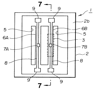
As shown in Figs. 1 to 4, a sensor device 1 has a
substantially square silicon substrate 2 whose one side is
about 3 mm long.
A front surface 2a, i.e., a first surface, of the
silicon substrate 2 is covered with an infrared ray
reflecting film 4 for reflecting infrared radiation except
for the portion thereof which forms an infrared ray
transmitting window portion 3. The infrared ray reflecting
film 4 is made of gold, platinum, silver, aluminum, titanium
or molibdenum, chromium and is 50 nm to 2000 nm thick.
Various methods, such as vapor deposition, sputtering, ion
plating, ion beam sputtering, CVD process (chemical vapor
deposition process) and plating, can be used for forming the
infrared ray reflecting film 4. The infrared ray
transmitting window portion 3 is covered with a film 4a
which prevents a incident infrared ray reflecting. The
film 4a is made qf ZnS, ZnSe and LiF, and 0.1~ 30 ~ m
thick. Various methods, such as vapor deposition,
sputtering, ion plating, ion beam sputtering, CVD, can be
used for forming the fiIm 4a.
A rear surface 2b, i.e., a second surface, of the
silicon substrate 2 has a hole portion 5 having
substantially upright side walls and a flat bottom wall at
a center thereof. Two parallel bridges 6A and 6B are
respectively laid across the hole portion 5. Each of the
1 3
20~0631
bridges 6A and 6B is a silicon oxynitride film having a
width of 100~ m. a length of 2mm and a thickness of 2 ~ m.
The silicon oxynitride film which forms the bridges 6A and
6B is also formed on the rear surface 2b of the silicon
substrate 2 except for the hole portion 5. That is, the
rear surface 2b of the silicon substrate 2 is level with the
surface of the bridges 6A and 6B.
- Infrared ray detecting elements 7A and 7B are
respectively provided on the bridges 6A and 6B at the
central protion thereof. Each of the infrared ray
detecting elements 7A and 7B is a fiIm made of amorphous
silicon (a-Si), polycrystal silicon or germanium (for
example; amorphous germanium(a-Ge)) and having a thickness
of 100 to 3000 nm. An amorphous germanium is preferably
used for the infrared ray deteting elements 7A and 7B in
order to be joined to electrode lines 8 and to get a large
coefficient of B. The B is shown by below formula;
R = Ro exp(B/ (l/T-l/To) )
where To is O K. T is an absolute temperature( K), Ro is
a resistance value at O K and R is a resistance value at T
K.
Various methods including sputtering, ion beam
sputtering and CVD process can be used to form the infrared
ray detecting elements 7A and 7B. The infrared ray
transmitting window portion 3 is formed in the infrared ray
reflecting film 4 at a position where it allows infrared
1 4
-- 204~631
radiation to enter only one infrared ray detecting element
7B. Therefore, the infrared radiation which passes through
the infrared ray transmitting window portion 3 is not made
incident on the other infrared ray detedting element 7A at
all.
Electrode lines 8 are respectively led from the
infrared ray detecting elements 7A and 7B along the bridges
6A and 6B. The electrode lines 8 are respectively connected
to electrode pads 9 formed at the peripheral portion of the
silicon substrate 2. The electrode lines 8 and the
electrode pads 9 are each formed of titanium, molibdenum,
aluminum, chromium, copper, nickel, tantalum, tungsten or
polysilicon to a thickness of 50 to 4000 nm using
sputtering, ion beam sputtering or CVD process.
The sensor device 1 having the above-described
configuration is fixed to a terminal substrate 11 having
four terminal pins 10, as shown in Figs. 5 and 6. An upper
surface 11a of the terminal substrate 11 has a hole portion
12 which is slightly larger in size than the hole portion 5
in the silicon substrate 2. Also, the upper surface 11a of
the terminal substrate 11 has conductive layers 13 formed
around the hole portion 12 at positions corresponding to
the electrode pads 9 of the silicon substrate 2. The
conductive layers 13 are electrically connected to the upper
end portions of the terminal pins 10, respectively. An
adhesive 14 made of, for example, an epoxy resin is coated
2040631
on the rear surface 2b of the silicon substrate 2 on the
peripheral portion thereof, by which the silicon substrate
2 is adhered and mechanically fixed to the upper surface 11a
of the terminal substrate 11 at a predetermined position.
At the same time, the electrode pads 9 of the silicon
substrate 2 are respectively laid on and electrically
connected to the conductive layers 13 of the terminal
substrate 11 by means of soldering or the like.
The silicon substrate 2 may also be joined to the
terminal substrate 11 using anode process or solder sealing.
If jointing work of the silicon substrate 2 to the terminal
substrate 11 is conducted in a vacuum, the infrared ray
detecting elements 7A and 7B can be held in a vacuum.
Jointing work of the silicon substrate 2 to the terminal
substrate 11, which is conducted in an inactive gas, such
as nitride, helium or argon, allows the infrared ray
detecting elements 7A and 7B to be held in the inactive gas.
In the infrared ray sensor arranged in the manner
described above, the infrared ray detecting elements 7A and
7B are provided on the rear surface 2b of the silicon
substrate 2, and the infrared ray reflecting film 4 with
the infrared ray transmitting window portion 3 formed in
opposed relation to the infrared ray detecting element 7B
is coated on the front surface 2a of the silicon substrate
2, as stated above. Infrared radiation which enters the
infrared ray transmitting window portion 3 passes through
1 6
2~406~1
the silicon substrate 2 and is then made incident on the
specified infrared ray detecting element 7B alone. It is
therefore possible to make infrared radiation enter only one
infrared ray detecting element 7B and to make no infrared
radiation to enter the other infrared ray detecting element
7A at all.
Consequently, it is not necessary to provide an
infrared ray reflecting film on the bridge in order to
block infrared radiation, unlike the conventional sensor
element, and the individual infrared ray detecting elements
can thus be held under the same environments. As a result,
a stable output which is not affected by the disturbance
can be obtained by calculating the difference between the
output of the infrared ray detecting element 7B on which
infrared radiation is made incident and that of the
infrared ray detecting element 7A on which no infrared
radiation is made incident.
Purthermore, in the above-described infrared ray
sensor, since the electrode pads 9 electrically connected
to the infrared ray detecting elements 7A and 7b are formed
on the rear surface 2b of the silicon substrate 2, the
sensor substrate 2 can be ioined to the terminal substrate
11 on which the conductive layers 13 are formed at the
positions corresponding to the electrode pads 9 in a face
down bonding fashion. This facilitates taking out of the
output of the infrared ray detecting elements 7A and 7B, and
1 7
2U~0~3~
reduces the overall size of the infrared ray sensor.
Purthermore, the upper surface of the terminal
substrate 11 to which the silicon substrate 2 is joined has
the hole portion 12, and the hole portion 12 is completely
sealed when the silicon substrate 2 is joined to the
terminal substrate 11. Also, this jointing work is
conducted in a vacuum so that the infrared ray detecting
elements 7A and 7B can be sealed in a vacuum. Consequently,
heat insulation between the infrared ray detecting elements
7A and 7B and the air can be enhanced, and the sensitivity
and accuracy of the infrared ray sensor can thus further be
mproved.
Furthermoe, in the above-described infrared ray sensor,
the bridges 6A and 6B are of the single layer type and are
formed of silicon oxynitride which assures balanced stress.
Consequently, the difference in the coefficient of thermal
expansion between the bridges and the silicon substrate can
be substantially reduced to zero. This provides a stable
bridge sutrcture and eliminates breakage of the bridges
which would otherwise occur during the manufacturing process.
Figs. 7(A) to 7(F) show the manufacturing process of
the infrared ray sensor according to the present invention.
First, the silicon substrate 2 having a face direction
(110) was prepared, as shown in Fig. 7(A). Next, a silicon
oxynitride film (SiO ~ N y ) 15 was formed on the two
surfaces of the silicon substrate 2 to a thickness of 2~ m
1 8
20~0631
by plasma CVD process, as shown in Fig. 7(B). That is, the
silicon substrate 2 was heated to 450 ~, and then vapor
growth of silicon oxynitride on the silicon substrate 2 was
performed under a pressure of 0.45 Torr using as the
reactive gas monosilane (SiH 4 ), nitride (N2) and laughing
gas (N20). The high frequency output was 400W. The flow
rates of nomosilane, nitride and laughing gas were
respectively 15 SCCM, 203 SCCM and 32 SCCM.
The thus-formed silicon oxynitride film 15 was analyzed
by Rutherform backscattering spectrometry. The composition
of the film was SiO,.20No. 677.
Subsequently, the silicon oxynitride films were
patterned to obtain the bridge patterns 6A and 6B shown in
Fig. 1. This patterning may be conducted until the silicon
substrate 2 is exposed by, for example, reactive ion
etching (RIE). Methan trifluoride (CHF3) and oxygen (02)
were used as the etching gas. The flow rate of the methan
trifluoride was 47.5 SCCM, and that of oxygen was 2.5 SCCM.
The pressure applied during the etching was 0.075 Torr and
the high-frequency output was 150W. Etching continued
three hours.
Therefore, the infrared ray detecting element 7B shown
in Fig. 7(C) was respectively formed on the bridges 6A and
6B at the central portion thereof. That is, an amorphous
germanium (a-Ge) was formed on the silicon oxynitride film
15 and the silicon substrate 2 by conducting sputtering
20~063~
using germanium as the target. Argon (Ar) and hydrogen (H2)
were used at the flow rate of 2 SCCM and 1 SCCM. The
pressure was 3-x 10 -3 Torr, and the high-frequency output
was 200W. Sputtering continued for ten minutes.
Next, annealing was conducted at 500 ~ for 20 minutes
to make amorphous silicon polycrystalline. Subsequently,
the polycrystralline silicon film was patterned by reactive
ion etching. Therefore, the electrode pads 9 shown in Fig.
7(D) were formed by forming an aluminum fiIm on the surface
of the silicon substrate 2 by vapor deposition and then by
patterning the film.
Next, the silicon substrate 2 located below the bridges
6A and 6B was selectively removed by etching to form the
hole portion 5 shown in Fig. 7(E). This etching was
anisotropic etching which used aqueous solution of
hydrogine. This anisotropic etching may also use aqueous
solution of potassium hydroxide.
Next, after the silicon oxynitride film 15 formed on
the front surface 2a of the silicon substrate 2 was removed
by etching, the infrared ray reflecting film 4 was formed on
the front surface 2a of the silicon substrate 2 by, for
example, deposition, as shown in Fig. 7(F). The infrared
ray reflecting film 4 may be made of platinum. Thereafter,
the infrared ray tranmitting window portion 3 was formed in
the infrared ray reflecting film 4 by the known
photolithographic technique at a position where it faces
2 O
20~631
the infrared ray detecting element 7B on the bridge 6B. The
coefficient B was about 4000K.
Fig. 8 shows the relationship between the gas flow
rateratio (N2/(N2+N20)) when the silicon oxynitride 15 is
formed and the yield of the bridge formation. As can be
seen from the graph, the highest yield was obtained when
the flow rate ratio was 0.865. At the time, the efficiency
was about 75%. At a flow rate ratio of 0.870 or above, the
silicon substrate 2 was curved after annealing which was
conducted at 500 C.
In case that amorphous silicon is used as infrared ray
detecting elements, the manufacturing process in Figs. 7(C)
~ 7(E) is as follows;
The infrared ray detecting element 7B shown in Fig.
7(C) was respectively formed on the bridges 6A and 6B at
the central portion thereof. That is, an amorphous silicon
(a-Si) was formed on the silicon oxynitride film 15 and the
silicon substrate 2 by conducting sputtering using silicon
as the target. Argon (Ar) and hydrogen (H2) were used at
the flow rate of 2 SCCM and 1 SCCM. The pressure was 3 x
10 -3 Torr, and the high-frequency output was 200W.
Sputtering continued for ten minutes.
Next, annealing was conducted at 1100C for 20 minutes
to make amorphous silicon polycrystalline. Subsequently,
the polycrystralline silicon film was patterned by reactive
ion etching. Therefore, the electrode pads 9 shown in Fig.
2 1
2040631
7(D) were formed by forming an aluminum film on the surface
of the silicon substrate 2 by vapor deposition and then by
patterning the film.
Next, the silicon substrate 2 located below the bridges
6A and 6B was selectively removed by etching to form the
hole portion 5 shown in Fig. 7(E). This etching was
anisotropic etching which used aqueous solution of
hydrogine. This anisotropic etching may also use aqueous
solution of potassium hydroxide.
Next, after the silicon oxynitride film 15 formed on
the front surface 2a of the silicon substrate 2 was removed
by etching, the infrared ray reflecting film 4 was formed on
the front surface 2a of the silicon substrate 2 by, for
example, deposition, as shown in Fig. 7(F). The infrared
ray reflecting film 4 may be made of platinum. Thereafter,
the infrared ray transmitting window portion 3 was formed
in the ray reflecting film 4 by the known photolithographic
technique at a position where it faces the infrared ray
detecting element 7B on the bridge 6B. In this case, the
coeficient B was about 3500K.
The case that amorphous germanium is used, annealing
may be not conducted. Also, annealing at more than 500 ~,
is not desired. If annealing is conducted its temperature,
the film 4a comes off. There is an advantage in the case
that amorphous germanium is used. The advantage is that the
electrode can be previously formed because of the low
20~06~1
anneal temperature.
The present embodiments are illustrative and not
restrictive, and various changes in the present invention
may therefore be resorted to without departing from the
spirit of essential characteristics thereof. For example,
in the above-described embodiments, the bridges 6A and 6B
have a linear configuration and are supported at the two
points. However, they may be supported at three points in
order to increase the strength thereof. Also, the bridges
6A and 6B are formed flat on the surface of the silicon
substrate 2 in the above embodiments. However, they may
have an arcuate form.
In the above-described embodiments, the silicon
substrate 2 was used as the sensor substrate which
transmits infrared radiation. However, a germanium
substrate may also be used. Furthermore, the surface 2a of
the silicon substrate 2 may be formed in a lens-like shape
so that the infrared radiation which enters the infrared
ray transmitting window portion 3 is converged to the
infrared ray detecting element 7B. Furthermore, three or
more infrared ray detecting elements may be provided.
Furthermore, in the above-described embodiments, the
bridges 6A and 6B were formed of silicon oxynitride.
However, it may be made of silicon oxide or silicon nitride.
Alternatively, the bridges 6A and 6B may have a multi-
layer structure.
2 3