Note: Descriptions are shown in the official language in which they were submitted.
20407 62
OPTICAL INTEGRATED CIRCUIT
The present invention relates to an optical
integrated circuit which has branched optical waveguides, and
more particularly to an optical integrated circuit which
permits direct mounting thereon of a photodetector, a light
emitting element, or similar optical active elements and can
be miniaturized.
Conventional optical integrated circuits will be
described hereinbelow in conjunction with the drawings.
It is an object of the present invention to provide
a miniature optical integrated circuit in which optical
waveguide terminals are sufficiently spaced apart to permit
direct mounting thereon of a photodetector and a light
emitting element.
In accordance with one aspect of the invention there
is provided an optical integrated circuit in which there are
formed on one face of an electrooptic plate first and second
optical waveguides extending at one end to one side of said
electrooptic plate and interconnected at the other ends and a
third optical waveguide connected at one end to the connection
point of said first and second optical waveguides, light beams
from said first and second optical waveguides being supplied
to coupled by said third optical waveguide and light from said
third optical waveguide being branched to said first and
second waveguides, wherein each of said optical waveguides
includes an end face, wherein the angle of said first optical
waveguide and said one side of said electrooptic plate is
deviated from 90, the end face of said first optical
waveguide at said one side forming a reflecting surface; and
wherein a fourth optical waveguide is provided on said one
face of said electrooptic plate, for guiding light reflected
by said reflecting surface to another side of said
electrooptic plate, different from said side thereof.
With such a structure as mentioned above, even if
the branched optical waveguides are formed short, that is,
even if the optical integrated circuit is formed
2040762
- -2-
small, the optical waveguide terminals are sufficiently
spaced apart so that active elements such as a
photodetector and a light emitting element can be mounted
directly on the optical integrated circuit.
BRIEF DESCRIPTION OF THE DRAWINGS
Fig. 1 is a plan view showing a conventional
optical integrated circuit;
Fig. 2A is a front view of an optical fiber
holder;
Fig. 2B is a top plan view of the optical fiber
holder;
Fig. 3 is a plan view showing the construction
of a conventional fiber optic gyro;
Fig. 4 is its sectional view;
Fig. 5 is a diagram schematically illustrating
an embodiment of the present invention;
Fig. 6 is a block diagram showing the
functional configuration of the fiber optic gyro
utilizing the optical integrated circuit depicted in Fig.
5;
Fig. 7 is a plan view illustrating an example
of the construction of the fiber optic gyro shown in
Fig. 6;
Fig. 8 is a side view of the fiber optic gyro
shown in Fig. 7;
Fig. 9 is a plan view illustrating a
transmitting-receiving module utilizing the optical
integrated circuit of the present invention; and
Fig. 10 is a front view of the module shown in
Fig. 9.
Fig. l shows a conventional optical integrated
circuit, indicated generally by 28. On an electrooptic
plate 11 as of lithium niobate (LiNbO3) there is formed an
optical waveguide 12, which has its one end branched into
optical waveguides 13 and 14 extending to optical
waveguide terminals 15 and 16 at one side of the
2040762
-- electrooptic plate 11 and has its other end branched into
optical waveguides 17 and 18 extending to optical
waveguide terminals 21 and 22 at the opposite side of the
electrooptic plate 11. Electrodes 23 are formed on both
sides of the parallel-extending portions of the optical
waveguides 17 and 18 near the terminals 21 and 22 to
provide an optical phase modulating function.
For input and output of light with respect to
such an optical integrated circuit, it is a common
practice in the prior art to employ a method in which an
optical fiber has its one end face fixedly bonded to each
optical waveguide terminal, or a method in which optical
fibers of the same number as that of the optical
waveguide terminals at one side of the electrooptic plate
11 are fixed to an optical fiber holder which is
connected to the optical integrated circuit.
Figs. 2A and 2B are a front view and a plan
view of an optical fiber holder for holding two optical
fibers. The optical fiber holder is composed of two
holder halves 24 and 25, which are assembled together to
fixedly hold two optical fibers 26 and 27 at one end
disposed in parallel as shown and their end faces are
ground or polished. The core spacing D2 of the optical
fibers 26 and 27 is equal to the outer diameter of each
optical fiber. Since the outer diameter of the optical
fiber is 125 ~m, for example, in the case of a single
mode optical fiber commercially available in Japan, the
spacing Dz is 125 ~m, for instance. Accordingly, the
distance D1 between optical waveguide terminals at one
side of the optical integrated circuit 28 is also
designed to be 125 ~m.
The angle of bend ~ at which the optical
waveguide is branched is several degrees or less in many
cases. Now, consider that the angle of bend ~ of the
branched optical waveguide 17 to the optical waveguide 12
is, for example, 1 in Fig. 1. In order that the spacing
D1 may be 125 ~m, the lengths L2 of those portions of the
2040762
_ 4
- branched optical waveguides 17 and 18 which are inclined
to the optical waveguide 12 are about 3.6 mm. In the
-~ case where the length ~ of the optical waveguide 12 is 7
mm, the length L5 of each of the parallel portions of the
optical waveguides 17 and 18 where the optical phase
modulating function is provided is 12 mm and the length L
of each of the parallel portions of the optical
waveguides 13 and 14 is 3 mm, the entire length L of the
optical integrated circuit is 29.2 mm.
The optical integrated circuit shown in Fig. 1
is used in a fiber optic gyro, for instance. Figs. 3 and
4 show an example of the fiber optic gyro, in which a
bobbin 32 with an optical fiber coil 33 wound thereon is
mounted on a chassis 29 covered with a cover 29, a light
source module 34 and a photodetector module 35 are
disposed inside the bobbin 32, a base plate 36 is
disposed on an upper plate 32A of the bobbin 32 and the
optical integrated circuit 28 is mounted on the base
plate 36 through a mounting plate 37.
Optical fiber holders 39 and 41, each holding
two optical fibers, are fixedly bonded to the two optical
waveguide terminals at the opposite sides of the optical
integrated circuit 28. The one optical fiber 42 held by
the holder 39 is connected by fusion to an optical fiber
43 extending from the light source module 34, whereas the
other optical fiber 44 is connected by fusion to an
optical fiber 45 extending from the photodetector module
35. Optical fibers 46 and 47 held by the holder 41 are
each connected by fusion to one end of the optical fiber
coil 33. Conventionally, the optical integrated circuit
and other modules are thus connected using optical
fibers.
In the optical integrated circuit 28 depicted
in Fig. 1, since the distance D1 between two optical
waveguide terminals is only 125 ~m or so, a photodetector
and a light emitting element, or an optical fiber holder
and a photodetector or light emitting element, each
20407 6~
_ 5
~- having a 1 mm or more chip size, cannot be mounted side
by side on the optical integrated circuit 28. To mount
the photodetector and the light emitting element side by
side on the optical integrated circuit, it is necessary
to increase the distance D1 between the optical waveguide
terminals, and this calls for an increase in the length L2
of each of the inclined portions of the branched optical
waveguides 13 and 14, inevitably making the optical
integrated circuit bulky.
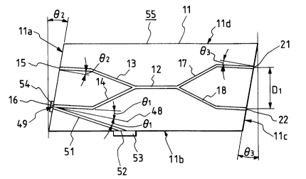
~ig. 5 illustrates an embodiment of the present
invention, in which the parts corresponding to those in
Fig. 1 are identified by the same reference numerals. In
this embodiment the terminal portion of the optical
waveguide 14 meets one side lla of the electrooptic plate
11 at an angle which deviates from 90; namely, the
optical waveguide terminal 16 of the optical waveguide 14
is inclined by an angle ~1 to a line 48 which is
perpendicular to the one side lla of the electrooptic
20~0~
-6-
-
plate 11. The end face of the optical waveguide 14 and
consequently the end face of the optical waveguide
terminal 16 forms a reflecting surface 49, which is
coated with a reflecting film 54 to ensure the reflection
by the reflecting surface 49. The reflecting film 54 can
easily be coated by the evaporation of aluminum. In this
embodiment there is formed an optical waveguide 51 by
which light reflected by the reflecting surface 49 is
guided to another side llb of the electrooptic plate 11.
To that end of the optical waveguide 51 which meets the
side llb of the electrooptic plate 11, that is, to an
optical waveguide terminal, there is fixedly bonded a
photodetector 53 which is a photoelectric transducer in
this example.
In the Fig. 5 embodiment the angle between the
side lla of the electrooptic plate 11 and the optical
waveguides 13 and 14 is deviated by ~2 from a right angle
and the angle of the side llc of the electrooptic plate
11 and the optical waveguides 17 and 18 is deviated by 93
from a right angle so as to preclude the possibility of
the occurrence of a Fresnel reflection on the end faces
of the optical waveguides and hence prevent the
occurrence of return light. The angles ~2 and ~3 each
differ with the refractive index of the optical active
element that is connected to the optical waveguide
terminal. In this example the angle between the optical
waveguide 14 and the side lla is deviated from a right
angle through utilization of the angle ~2 ~ and hence
= ~92-
The optical integrated circuit 55 of this
embodiment is of about the same size as that of the
conventional integrated circuit shown in Fig. 1, if the
optical fiber 125 ~m in diameter is used, that is, if the
7 20iO~fi2
distance Dl is 125 ~m.
Figs. 6 through 8 illustrates, by way of
example, the case where the optical integrated circuit 55
depicted in Fig. 5 is built in a fiber optic gyro. At
first, a light emitting element 56 is fixed directly to
the terminal 15 of the optical integrated circuit 55 as
shown in Fig. 6. The light emitting element 56 is driven
by a light source driver 57 and the resulting light
reaches the optical waveguide 12 via the optical
waveguide 13. The light having reached the optical
waveguide 12 is split to light beams which are guided the
optical waveguides 17 and 18, from which they propagated
through the optical fiber coil 33 in opposite directions.
The light beams having thus propagated through the
optical fiber coil 33 are coupled together by the optical
waveguide 12 to form interference light. The
interference light is branched to the optical waveguides
13 and 14 and the light branched to the optical waveguide
14 is reflected by the reflecting film 54 to the
photodetector 53 via the optical waveguide 51. A signal
resulting from the photoelectric conversion by the
photodetector 53 is amplified by an amplifier 58 and is
then applied to a signal processor 59 formed by a
synchronous detector. The input signal is processed by
the signal processor 59 and is provided therefrom as the
gyro output to a terminal 61. A phase modulator 62
formed on the optical waveguide 18 of the optical
integrated circuit 55 is provided for accurately
detecting input angular rate information which is
provided to the optical fiber coil 33. A phase
modulating voltage from a phase modulator driver 63 is
applied across the electrodes of the phase modulator 62.
Now, a description will be given, with reference
-8- 20407~2
to Figs. 7 and 8, of the construction of the fiber optic
gyro. The optical fibers 46 and 47 connected to the
optical integrated circuit 55 by means of the holder 41
are each fused to one end of the optical fiber coil 33.
The light emitting element 56 is connected to the optical
waveguide terminal 15 of the optical waveguide 13. It is
also possible, in this case, to form an optical waveguide
type lens (such as a mode index lens, geodesic lens, or
grating lens) near the optical waveguide terminal 15 of
the optical waveguide 13 so as to improve the coupling
between the light emitting element 56 and the optical
waveguide 13; The photodetector 53 is bonded to the
optical waveguide terminal 52 of the optical waveguide
51. Within a space 64 surrounded by the broken line
there is disposed the ceramic base plate 36 as of
ceramics, on which there are mounted the optical
integrated circuit 55 and a hybrid IC carrying the light
source driver 57, the amplifier 58, the phase modulator
driver 63, etc. shown in Fig. 6. In a space 65 inside of
the bobbin 32 there are disposed the photodetector module
and the light source module in the prior art example
depicted in Figs. 3 and 4, but in this embodiment the
photodetector 53 and the light emitting element 56 are
mounted on the optical integrated circuit 55, and
consequently the signal processor 59 and others can be
housed in the empty space.
Figs. 9 and 10 illustrates an example of another
embodiment of the present invention as applied to a
transmitter-receiver module. An optical inteqrated
circuit 66 is formed by the optical waveguides 12, 13, 14
and 51 of the optical integrated circuit 55 shown in Fig.
5. Light from the light emitting element 56 passes
through the optical waveguide 13 and enters into the
~ -9- 20 107~2
optical waveguide 12, from which it is provided on an
optical fiber 67 for transmission. On the other hand,
light transmitted over the optical fiber 67 enters into
the optical waveguide 12, from which it is branched to
the optical waveguides 13 and 14. The light branched to
the optical waveguide 14 is reflected by the reflecting
film 54 to the photodetector 53 via the optical waveguide
51. In a space 68 indicated by the broken line there are
disposed on a base plate 69 as of ceramics, together with
the optical integrated circuit 66, an electronic circuit
for driving the light emitting element 56 and a circuit
for amplifying the output signal from the photodetector
53, the both circuits being miniaturized through use of
hybrid IC pac~aging techniques. The circuits mounted on
the base plate 69 are hermetically sealed by a cover case
71 and each terminal 72 is a hermetic terminal.
In Fig. 5 the optical waveguide 51 may also be
formed so that its terminal 52 extends to the side llc of
the electrooptic plate 11. Also in such a case, the
terminal 52 and those 21 and 22 can be spaced a large
distance apart. The terminal 52 may also be extended to
another side lld of the electrooptic plate 11. In this
instance, the optical waveguide 51 crosses other optical
waveguides, but this can be implemented by sufficiently
reducing its coupling with the crossed optical
waveguides. The reflecting surface may also be formed on
the end face of the optical waveguide 13 in place of the
end face of the optical waveguide 14 and its terminal may
be guided to another side of the electrooptic plate 11.
Similarly, one terminal of each of the optical waveguides
17 and 18 may be positioned at another side of the plate
11 .
As described above, according to the present
-lO- 20~0~62
invention, a photodetector, light emitting element or
optical fiber can be connected directly to an optical
integrated circuit with branched optical waveguides by
employing a structure in which light in one of the
branched optical waveguide is reflected by an end face of
the optical integrated circuit to another end face
thereof. In addition, the optical integrated circuit can
be made small. This permits miniaturization of devices
using the miniaturized optical integrated circuit, such
as a fiber optic gyro and a transmitter-receiver module.
It will be apparent that many modifications and
variations may be effected without departing from the
- scope of the novel concepts of the present invention.