Note: Descriptions are shown in the official language in which they were submitted.
204 1 223
BACKGROUND OF THE INVENTION
The present invention relates in general to a functional
programmable PCM (pulse code modulation) data analyzer and
transmitter for use in telecommunications equipment.
In general PCM data analyzers look at signal characters
such as voltage, power, frequency, DTMF detection and a
variety of other characteristics of information in the digital
telecommunication system. These devices usually connect
externally to the telecommunications equipment. Such external
equipment requires analog conversion and the circuitry of such
equipment often requires programming to perform specific
functions when installed in a switch of a telecommunications
system.
The present invention overcomes these drawbacks of the
prior art and provides a data analyzer and transmitter which
is integrated in the telecommunications equipment and further
which is programmable so that it may address different
functions at different times.
.
-- 204 1 223
SUMMARY OF THE INVENTION
It is an object of the present invention to provide a
digital signal processing system for interfacing with a means
for central control having at least a control port. The
present invention has a control means for processing having
an interface port connected to the control port of the central
control. The means for processing also has at least first,
second and third ports. At least first, second and third
kernel means for running software application tasks have
first, sec,nd and third ports, respectively, connected to the
first, second and third ports of the control means for
processing, respectively. Each of the kernel means has a
plurality of channel ports connected to a bus means for
providing a plurality of channels. The control means for
processing in response to data received from the central
control establishes one of a plurality of software application
tasks in each of the kernel means. The bus means carries at
least 24 channels, each of the kernel means communicating with
8 channels of said 24 channels such that each kernel means
receives different channels than channels received by ot~er
kernel means. The 24 channels are pulse code modulated and
204 1 223
designated 0 through 23, the first kernel means communicating
with channels 0, 1, 6, 7, 12, 13, 18 and 19, the second kernel
means communicating with channels 2, 3, 8, 9, 14, 15, 20 and
21 and the third kernel means communicating with channels 22,
23, 4, 5, 10, 11, 16 and 17. Each of the kernel means have
their respective channel ports connected to the bus means by a
means for multiplexing/demultiplexing such that each of the
kernel means communicates with its respective channels of the
24 channels.
lo Each of the kernel means has a means for processing and
the software application tasks include at least one of the
DTMF (dual tone multifrequency) detection, MF multifrequency
detection and metering. Each of the kernel means is
separately assigned any one of the application tasks by the
control means for processing.
,~
204 1 223
In accordance with an embodiment of the invention,
a digital signal processing system for interfacing with a
central control having at least one port, is comprised of
apparatus for processing having an interface port connected
S to the port of the central control and at least first,
second and third ports; a serial multiplex communication bus
for carrying at least n x 6, where n is a whole number,
channels on a synchronous time division basis; at least
first, second and third kernels for running software
application tasks having at least first, second and third
ports, respectively, connected to the at least first, second
and third ports of the processing apparatus, respectively,
each of the kernels having a channel port connected to the
serial multiplex communication bus; apparatus for selecting,
in sequence, each of the kernels for intermittent
communication with the serial multiplex communication bus to
cause each of the kernels to continuously communicate with
two successive channels for every six channels occurring on
the serial multiplex communication bus; and the processing
apparatus receives data from the central control and in
response to the data selectively (a) transfers the data to
the kernels and (b) processes the data without transferring
the data to the kernels.
- 4a -
p~ :
,.~..,.~
- 204 1 223
In accordance with another embodiment, a digital
signal processing system for interfacing with a central
control having at least one port, is comprised of apparatus
for processing having an interface port connected to the
port of the central control and at least first, second and
third ports; a serial multiplex communication bus for
carrying a preselected plural number of channels on a
synchronous time-division basis; at least first, second and
third kernels for running software application tasks having
at least first, second and third ports respectively,
connected to the at least first second and third ports of
the processing apparatus, respectively, each of the kernels
having a channel port connected to the serial multiplex
communication bus; apparatus for selecting, in sequence,
each of the kernels for continuous communication with
channels on the serial multiplex communication bus; the
processing apparatus responsive to data received from the
central control to establish one of a plurality of software
application tasks in each of the kernels, the software
application tasks being downloaded from the central control
to each of the kernels via the processing apparatus; and
each kernel communicating with a preselected number of the
channels of the serial multiplex communication bus, each
kernel communicating with channels different than the
plurality of channels with which the other kernels
communicate.
- 4b -
- 204 1 223
In accordance with another embodiment, a
telecommunication system with a synchronous time division
serial multiplex communication bus having n x 6, where n is
a whole number, channels and an automatic call distributor
S having a central control, the improvement being a pulse code
modulation data analyzer, is comprised of programmable
apparatus for processing electrically coupled to the central
control and responsive to data from the central control; at
least three kernel programmable apparatus for processing
electrically coupled to the programmable processing
apparatus, each of the kernel programmable processing
apparatus selectively, individually responsive to data from
the programmable processing apparatus; apparatus for
sequentially selecting each of the kernel programmable
processing apparatus for intermittent communication with the
bus to continuously receive two successive channels for
every six channels occurring on the bus; and apparatus at
each of the at least three kernel programmable processing
apparatus for analyzing signal characteristics of the at
least two successive channels received by the respective
kernel programmable processing apparatus.
- 4c -
`_- 204 1 ~23
BRIEF DESCRIPTION OF THE DRAWINGS
The features of the present invention which are believed
to be novel, are set forth with particularity in the appended
claims. The invention, together with further objects and
advantages, may best be understood by reference to the
following description taken in conjunction with the
accompanying drawings, in the several Figures in which like
reference numerals identify like elements, and in which:
FIG. 1 is a general block diagram of the present
invention in the environment of a telecommunications system;
FIG. 2 is a more detailed block diagram of the present
nventlon;
FIG. 3 is a further more detailed block diagram of the
control portion and of one of the DSP kernels;
FIG. 4 is a block diagram schematically illustrating
the interface between the control kernel and one of the DSP
kernels.
,~,~.
204 1 223
-
DESCRIPTION OF THE PREFERRED EMBODIMENT
The present invention has general applicability, but is
most advantageously utilized in digital signal processing
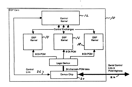
embodied on a Digital Signal Processing (DSP) Card, as shown
in Figure 1. In a preferred embodiment, the Digital Signal
Processing Card 10 provides DTMF and MF detection, and other
functions. A typical automatic call distribution (ACD)
application will consist of one DSP card with another one as a
backup. The Digital Signal Processing backup card can be used
as a digital multimeter for system connection to various lines
for testing purposes, while a card such as a Digital Audio
Source (DAS) backup card can be used for message recording and
editing.
For clarity, the Network control structure that is
outside of the DSP card is referred to herein as a Central
Control 20. The control kernel 30 on the card 10 comprises a
68000 microprocessor 12, and the three application
microprocessors 14, 16, 18 on the card are referred to as DSP
kernels.
Each of the three DSP kernels 14, 16, 18 on the DSP card
10 can be configured for one of several functions. Three of
these functions, MF detection, DTMF detection, and metering
,
..
20412~`3
are included in the preferred embodiment of the present
invention, and a path is provided for adding new features to
this same hardware by later software additions.
The DSP card 10 can support any combination of 3 software
applications per card. For example, the Digital Signal
Processing Card lo can be assigned by Central Control 20 to
be either three applications of DTMF detection, three
applications of MF detection, or a mixture of three different
applications. The term application will refer to the code
running in each DSP kernel. Each application will service
more than one channel. After the Central Control 20 downloads
software to the DSP kernels 14, 16, 18 each kernel
continuously monitors each hardware assigned channel. Upon
completion of the application task, the DSP kernels report
their results to the 68000 microprocessor 12. The 68000
microprocessor 12 may then respond to the Central Control 20.
In the ACD environment, where only a small number of DTMF
detection channels are required, a typical configuration would
be one DTMF, one MF, and one meter application on a single
card. There would be only one card in the system with one
backup card.
204 1 223
In a tandem switch environment where a larger number of
channels of both DTMF and MF are required, each card might be
configured with three applications of either DTMF or MF, and a
dozen or so cards would reside in a system. Again, one card
could be a backup.
The Central Control 20 referred to herein is any part of
the control structure which resides outside of the DSP card 10
(see Figure 1). The card represents a three section
programmable resource of the Central Control. There is a
control microprocessor 12 (MC68000) on the DSP card 10 which
controls the entire card including handling mail information
to the Central Control 20, access to a serial control link
(not shown), control of the three DSP kernels, 14, 16, 18 and
collection of dial pulse information.
Each DSP kernel 14, 16, and 18 comprises a
microprocessor 36, memory 38, an interface to the 68000
microprocessor, and an interface with a PCM highway. Each of
the three DSP kernels can be downloaded with one of several
applications. The three applications can be, for example:
DTMF detection for 8 channels; MF detection for 8 channels;
and digital multimeter function for 8 channels.
:~`
204 1 223
The DSP card 10 shown schematically in Figure 2, will
appear to a Central Control System as the number of channels
proportional to the number of applications that have been
downloaded. When, for instance, a DTMF register is required
at the Central Control level, the list of available registers
will be checked, and one will be assigned. This command is
received by the 68000 microprocessor 12, which issues a
command to the appropriate DSP micro on the card. The DSP
micro, that is one of the three DSP kernels 14, 16, 18, then
lo assign a detector and upon reception of a valid digit, returns
the digit code to the 68000 microprocessor 12. The 68000
microprocessor 12 has the option of collecting digits before
reporting them to the Central Control 20. If after a certain
time out when no valid digits are received by the DSP micro,
the 68000 microprocessor 12 may notify the Central Control 20.
The DSP micro assigned by the 68000 microprocessor 12 may then
be either deallocated or allowed to continue longer.
Figure 2 illustrates communications with the DSP card 10
over the multiplexed Serial Highway 22. The 24 channel PCM
data as well as the Control Link information pass over the
link 26. A custom multiplexing and demultiplexing network
line interface integrated circuit 24 (NLI IC) performs these
,
- '
204 1 223
operations. The 24 channels of PCM data are then further
demultiplexed by logic demultiplexer 25 to connect to the
three DSP kernels 14, 16, 18.
Before going into the functional description, a few
terms will be defined. The term firmware applies both to the
program code in the DSP kernels, 1, 16, 18 and for the 68000
microprocessor 12 which interfaces to hardware elements (the
I/0 interface). This code is rudimentary in nature and all
application programs (such as DTMF, MF, or others) will
interface with this code in a similar fashion. Thus 2 types
of firmware exist; C25 firmware and 68000 firmware.
The term software, on the other hand, signifies an
application program which, excluding any ties with I/0, is
independent of the hardware arrangement. Thus, software is
the actual application task which will be run by the
microprocessor on the card.
The software that resides on the DSP card for the 68000
microprocessor is responsible for several control items. The
68000 microprocessor must handle communications with the
Central Control 20 through the NLI IC 24 receive and transmit
buffers.
204 1 223
The 68000 microprocessor also performs the functions
associated with collecting digit strings. Moreover, it must
accept A signalling from the NLI 24 over Serial Control Link
28 and can calculate the correct dial pulse sequence. During
initialization, it must download its own program and the
program for each DSP kernel.
It must also perform self diagnostics and be able to
identify a faulty DSP kernel and take appropriate action such
as resetting the DSP kernel. Each DSP kernel contains a
general purpose high speed digital signal processor which can
perform real time operations on digital data being received
over the PCM highway from the NLI. Thus, the kernel processor
can run numerous types of application tasks for the system.
The DSP kernel will also run self diagnostics to
validate both hardware and software integrity. The 68000
microprocessor will periodically order the DSP kernel to
perform program RAM contents validation, and expect the kernel
processor to respond accordingly with its findings.
As shown in Figs. 3 and 4, the 68000 microprocessor
communicates with the C25s through XCVR block 47 consisting of
registers 42, 44, 45 and 46. The 68000 microprocessor 12 will
monitor a status port 50 to communicate with the DSP kernels.
When a kernel processor writes data to the 16 bit register 42
for the 68000 microprocessor 12, a bit in the status port 50
204 1 223
will be active. The 68000 microprocessor 12 upon sensing this
activity will respond by reading the register to collect the
new information. The read operation will then reset the bit
and signal to the kernel processor that new data can be
written into the register.
When new data from the Central Control 20 arrive to the
DSP card 10, the NLI 24 will activate an interrupt to the
68000 microprocessor 12. The 68000 microprocessor 12 responds
while reading the NLI receive FIFO in the interrupt routine.
The kernel processor firmware is the program code which
resides at the DSP kernel that defines the hardware
environment of the TMS320C25 processors. After the software
is downloaded to the DSP kernel, the firmware will read and
write from the PCM data stream, receive instructions from the
68000 microprocessor, and return results to the 68000
microprocessor.
The kernel processor will monitor an input buffer
(status port 49) to communicate with the 68000 microprocessor.
When the 68000 microprocessor writes data to the 16 bit
register 44 of the kernel processor, a bit in the input buffer
(status port 49) will be a~tive.
12
204 1 223
The kernel processor upon polling this buffer for
activity should respond by reading the register 44 to collect
the new information. The read operation will then reset the
bit and signal the 68000 microprocessor that new data can be
written into the register 44.
An input pin of the kernel processor is used to detect
an 8 KHz framing pulse from the NLI 24. This signal, when
active, indicates that a new frame of information is starting
and that the software frame/channel counters should be reset
to zero.
The 68000 microprocessor kernel 30 consists of a 68000
CPU, 32K x 16 RAM, and 32K x 16 ROM. An additional 32K words
of RAM can be added to the card when memory chips and a
different PAL programmable array logic chip (DSPPALOB) are
added to the card. The primary information in the ROM is self
boot, link communication primitives, and diagnostic tests.
All the programs for the DSP kernel and the 68000
microprocessor will be downloaded through the NLI control link
interface which connects to the control complex. This
download capability allows maximum flexibility for software
changes at a later date. There are also registers for
communicating control information with the NLI 24, serial data
~.,
.b
204 1 223
-
for transmission, and the reception of PCM dial pulse data.
There are control registers to communicate with each of
the DSP kernels 14, 16, 18 as well as the capability to
perform real time direct memory access DMA functions to the
kernel program memory bank.
Each DSP kernel 14, 16, 18 appears to the 68000
microprocessor 12 at different memory addresses. This permits
the 68000 microprocessor 12 to load the program memory of each
DSP kernel 14, 16, 18 separately. An output register of the
68000 microprocessor 12 controls the reset and hold mode pins
of each DSP kernel 14, 16, 18 separately.
The 68000 microprocessor 12 has the capability to detect
or to mask bus errors while accessing external memory or
devices. If a data transfer acknowledgment from the external
device accessed by the 68000 microprocessor is not received
after a certain timeout period, a bus error will occur. This
will force an exception processing routine to occur on the
68000 microprocessor 12. An example of this occurrence
happens when the 68000 microprocessor 12 attempts to access
.,
204 1 223
the memory of a DSP kernel before the kernel is put into the
hold state. The bus error exception processing routine will
examine the contents of the stack to determine the location
of the mishap.
The 68000 microprocessor 12 also interfaces with a write
protect memory circuit. An 8 bit register can protect blocks
of 4K words of the 68000 microprocessor lZ x 32K ~ord RAM
memory. An additional 8 lines are available for the
protection of an additional 32K words of memory which can be
added on the card 10. Each of the three kernel processors 14,
16, 18 may interrupt the 68000 microprocessor 12.
The circuit configuration for all 3 DSP kernels are the
same. This commonalty prevents the occurrence of kernel
specific software which would limit the type of applications
executable on the card.
The DSP kernel comprisin~ a Tl1~320C25 (C25) digital
signal processor kernel with 4k x 16 high speed static ram,
control registers that allow the passage of 16 bit information
between the 68000 and the C25s, and address decoding.
The C25 separately addresses the 64K of program, data and
I/O space. Program space and some data space for the
.'t"
2~ 7 223
processor resides in the 4K of RAM in the kernel. Some data
space of the processor 36 exists internally in the processor,
providing 512 words of storage capability. The processor
accesses the I/0 space of the 16 bit read/write registers 42
and 44 selected by the I/0 decode block 51 for communicating
with the 68000 microprocessor 12 while not in the hold state
and a status port 49 determines if the 68000 microprocessor 12
has new information in the message register 44.
The microprocessor 12 has the capability of forcing a
hold mode on to the C25 processor. While in the hold mode,
the C25 processor halts program execution, and places all
address and data lines in a high impedance state. This mode
also enables the 68000 microprocessor 12 to access the program
memory of the C25 kernel.
The NLI kernel 27, comprising logic demux chip 25 and
demux chip 24, contains the circuitry necessary for the card
10 to communicate over the system backplane to a network shelf
controller (NSC). This allows the passage of control commands
and data to the card to indicate the tasks the card will
correspondingly perform and report. Usage of the NLI IC
(demux chip) 24 and a PCM commutating circuit (logic demux
chip) 25 allow the card to communicate with the rest of the
system.
16
- 204 1 223
On both receive and transmit serial PCM operations of
the C25, the commutating circuit 25 divides the PCM data into
groups of 2 channels that sequentially select each C25. Thus
the channels assigned to each C25 are fixed, and are in a
predetermined sequence. The commutating circuitry 25 contains
a counter which produces pulses to signal the C25 to begin
transmission or reception of PCM serial data. The NLI demux
chips 24 is an application specific integrated circuit (ASIC)
which contains the necessary logic for communicating, through
drivers and receivers, over the backplane.
The Serial Highway 22 contains multiplexed PCM data and
control data to and from the card. Although the control link
will contain bidirectional information, for descriptive
simplicity, control information will be assumed to flow from
the Central Control to the 68000 microprocessor 12, and Report
or Status information flows from the 68000 microprocessor 12
to the Central Control.
The software handles all the incoming and outgoing mail
for the DSP card. Mail queues are maintained for both
directions to assure orderly flow away from and toward the
card.
2~ 23
-
Inherent in the Digital Signal Processing card (as well
as all other cards that use the NLI bus) is the ability to
insert a PCM sample onto the "to switch" NLI bus and to
extract the PCM sample from the "from switch" NLI bus. As a
test of system integrity, digital test tones from the DAS
Module could possibly be sent over the network link to the DSP
Module for detection.
A register!transmitter pair will be acquired and tone
digits will be sent between the two. If the digits sent match
the digits received, there is a high probability that both of
the pair are functioning correctly. Since these digits will
be sent over the NLI buses and through a time slot
interchanger (TSI) card, a further test can be run using the
Pad/Gain feature of the TSI. This would involve adding pad
and/or gain to the transmitted digits and seeing if the
receiver still recognized the digit as valid. Both tests
between the DAS Module and the DSP Module could be run to
check system integrity.
The 68000 microprocessor kernel 30 must maintain contact
with each DSP kernel and with each channel. One way of
approaching this function would be to maintain a list of
status tables and report tables for each DSP kernel. The
18
204 1 223
68000 microprocessor 12 would check the status of each device
and take appropriate action.
The firmware is written to present a common format to
the software in the 68000 microprocessor 12. A one word
message can be sent between the 68000 microprocessor 12 and
the C25. When the 68000 microprocessor 12 resets a DSP
kernel, it will clear the message register flags invalidating
any data present.
This section deals with the protocols and data transfers
between the DSP card 68000 microprocessor 12 and TMS320C25
CPUs. As shown in Fig. 3, there are main interfaces between
the C25 and the 68000 CPUs.
First is the download interface comprising registers 45
and 46. This is only used for initial program load. The
68000 CPU resets the C25, puts the C25 CPU on hold and loads
its program memory with the application program intended. The
second is the status Port Interface comprising status ports 48
and 49. A status Port on each CPU is tied together and a
handshaking technique is used to ensure that communication is
positively transferred between the CPU's. This interface
will be used to transfer information while the C25 is running.
19
204 1 223
In the preferred embodiment there are 3 separate
application programs that may be downloaded from the 68000
microprocessor 12 to the C25. One is DTMF tone detection
program. This detects 40 milliseconds DTMF tones and reports
the events to the 68000 CPU. Another is MF tone detection.
This detects any of 15 combinations of 2 tones for MF tone
detection applications. Finally, there is metering. This
provides an AC or DC voltmeter as well as a frequency counter
for doing some analog testing in the switch. Each application
program is less than 1000 words.
All of the programs listed have a sanity test capability
(a check sum of the program memory) that may be run in a
background mode. The main task of the C25 is to perform one
of the real time functions listed above. Each program is time
multiplexed providing an 8 channel capability. All 8 channels
associated with a given C25 will be dedicated to performing
the same task. That is to say you cannot have 4 channels of
DTMR and 4 channels of metering on a single C25.
The C25 program uses almost all of its available RAM and
most of the CPU time. As a result the C25 operation system
,,
-- 204 1 223
is very simple. The PCM samples are stored in an elastic
buffer during the real time interrupt. A background mode of
operation provides for the 68000 CPU interface routines and
the execution of the downloaded program.
Real time interrupts occur every 31.25 microseconds.
About 2 microseconds of each interrupt are required to store
the PCM samples. When interrupt routine is completed, and the
background tasks will be executed. The interrupt handling
routines should be a minimum of '0 instruction cycles long to
avoid re-execution of the interrupt routines since interrupts
on the C25 are both edge and level sensitive and the interrupt
pulse is 970 nanoseconds long. Thus if the interrupt handler
completes its task in under 10 cycles, another interrupt
process will occur.
When a background task is completed, the C25 will return
to an idle loop to find a new task. The tasks will be
prioritized in the following order:
1) Process PCM samples. If there is an unprocessed PCM
sample in the elastic buffer, the sample will be
processed according to the application that has been
downloaded.
2) Service 68000 I/O requests. The I/O status register 49
will be checked for an instruction from the 68000
and put in a command queue.
f~. ~
204 1 223
3) Check sum testing. If there are no other tasks then
a few words of program memory are check summed.
Initialization of the 3 C25 processors begins with the
reception of the POR (Power on Reset) signal from the NLI.
The POR~signal automatically causes all C25s to enter both a
reset and hold state. After the 68000 microprocessor 12 fully
loads software code from the control complex, it will begin
loading each 4K program/data space of the C25s. Upon
completing program load, the 68000 will release control of
the reset 52 and hold 53 lines of the C25s, shown in Fig. 4,
a]lowing pro~ram execution to begin at address>OOOO.
The beginning software code that the C25 runs will start
by initializing the status registers ST0 and STl of the C25.
The following is a list of register settings for a preferred
hardware arrangement:
F0=0 Configures serial ports to 16 bits.
Command: FORT 0
HM=1 C25 executes in~hold mode.
Command: SHM
ITM=0 Enables interrupts. Allows serial port operations.
Command: EINT
IMR=>0010 Enables serial port recv int, disables NLI
clock int and trx serial int (unused)
Command: load data loc 0004 with>0030
204 1 223
FSM=1 Frame pulses required for serial port operation.
Command: SFSM
TXM=0 Transit frame pulse in an input.
Command: RTXM
Another process that the C25 will complete is the
loading of data space memory which is internal to the C25 with
constants from the program space memory. The TBLR instruction
will allow the transfer of this information into the C25 data
space.
Other software commands allow C25 to utilize I/O space
for communicating with the 68000 master processor. The C25
has 2 input ports and 1 output port for accomplishing this
task. Input port 0 and output port 0 are two 16 bit
registers 44 and 42 respectively which allow data transfer
between the 68000 and C25 while both are processing
information. Input port 1 acts as a status register 49 for
the C25 which controls the transfer operation of the C25 so
that no information is lost.
When the C25 write:; data with OUT 0 to the data register
42 for the 68K, a bit is reset with a flip flop to signal to
the 68K that data is available. When the 68K reads this
location, the flip flop will set indicating that more data can
be sent. This bit can be read by the C25 and is INP 1, bit 1.
2~A1223
Likewise, when the 68K writes a word to the C25, bit 0
of input port 1 is reset. The C25 periodically polls this
port to determine if information is available by testing for
bit 0 being 0. The following is a sample of C25 software
which performs this function:
IN STAT, 1 ; STORE TRANSFER STATUS IN DATA MEM
LOCTN
LAC STAT ; PUT TRANSFER STAT IN ACCUMULATOR
ANDK >0001 ; CHECK FLAG FOR DATA FROM 68K.0=TRUE
BGZNO_MSG
IN68K_RD,0 ;READ I/0 PORT 0 FOR MESSAGE AND STORE
'
NO_MSG: .
(CONTINUES)
PCM data transfers serially between the NLI and the C25.
The C25 receives and transmits an assigned group of
channels as set in hardware:
Table 1. Channels Used with NLI
C25A 0, 1, 6, 7, 12, 13, 18, 19
C25B 2, 3, 8, 9, 14, 15, 20, 21
C25C 22, 23, 4, 5, 10, 11, 16, 17
Thus, each C25 will receive 8 channels of information.
This PCM data loads as 16 bits (2 channels) into the C25,
where the lower numbered channel is in the high byte of the
DRR-data receive register. Once this register fills, an
24
`~ 204 1 223
interrupt will occur, and the two channels of PCM are
available in the DRR for processing. The C25 is interrupted
every 31.25 microseconds with new channel information to
receive and to transmit. There is a channel timing offset
between receive and transmit functions and these interrupt
functions do not occur simultaneously. The C25 synchronizes
the reception of PCM by the use of an I/0 pin, the BI0, on the
processor.
The BI0 pin is a software testable I/O pin which the C25
uses to test for the beginning of the frame. This pulse
occurs every 125 microseconds with an approximate duration of
647 nanoseconds. The C25 will monitor the status of the BI0
pin, in a short loop since the frame pulse is only 970
nanoseconds long, to determine when the frame begins and to
reset internal software channel counter.
There is a channel count difference between the receive
channels and the transmit channels, thus 2 synchronizing frame
inputs connect to the processor.
As shown in Fig 3, the DSP card is divided into three
main subsections plus the power supply (not shown). They are
the DSP kernels, the 68000 kernel, and the NLI kernel and
. .
- 204 1 223
interface. The 68000 performs intelligent queuing of messages
and communicates with the Central Control system via the
serial link 28. It controls the input to the DSP kernels.
The 68000 processor is in charge of distributing the
request message from the mail boxes to the appropriate
locations in the DSP kernels, monitors the kernels' report
registers for completed tasks. The processor will also check
for immediate change of status request on each channel issued
by the Central Controller and transfers this status request to
the appropriate operating channel.
Figures 3 and 4 pictorially illustrate the circuitry
blocks for downloading program memory contents to the DSP
kernels. The hold signal places the C25 in a high impedance
state and activates the hold acknowledge line 43 shown on Fig.
4 which puts the C25 memory into the 68000 memory map. ROM 34
is provided as 32K x 16.
Program memory 33 for the 68000 microprocessor 30 is
provided as 32K x 16 RAM 32 and ROM 34. It is word or byte
accessible. Expansion to 64K words is possible with 2
additional 32K x 8 RAM chips and replacement of DSPPALOA with
DSPPALOB. DSPPALOA does not produce a chip select for the
operational RAM space.
20~1223
,~
Each TMS320C25 processor 36 has 4K words of memory which
can be accessed as program or data space by the C25. A 4K X
16 memory bank 38 switches into the 68000 address spectrum
when the 68000 places the DSP processor in a hold state. The
68000 may then read or write to the contents of the C25 memory
in word access format. It is advisable that the 68000 put the
C25 into the reset mode after downloading new program material
in order to place the C25 into a new known state. Attempts
to write to these areas of memory without activating the hold
bit for the kernel will result in a bus error. This memory
is only word accessible to the 68000. Incorrect data
transfers will occur if byte access operations happen in this
memory space.
A 82C55 I/O port 40 is used for enabling write protection
of RAM memory. Each I/O line protects 4K words of memory from
unauthorized write operations. This part is initialized with
80H to address OEOOC6H after a reset occurs. After which,
writing a bit '1' at OEOOC2H or at OEOOC4H will protect a
given 4K block of RAM memory when the write protect function
is active. When a write cycle attempts to access a protected
memory location, a bus error will occur to inform the
2~4 1 2~3
processor of the violation. The 82C55 registers as well as
protected memory can be read at any time. Writing to a
protected memory area while the write protect lock is active
or to ROM will result in a timeout bus error.
There are provided 16 bit data registers 42, 44 for
communicating between the 68000 and the DSP kernels. One set
is for reading contents and the other register is for writing
data. A processor will not read the same contents as are
written to the register since they are distinct. Each DSP
kernel has an associated set of registers 42 and 44 for
transferring data. The registers are not read or written to
before an examination of the appropriate bit in the
interprocessor registers 48 and 49.
The C25 status port 50 ,coordinates the transfer of
information between the 68000 and the DSP processors on the
card. This register is only readable. The bits in the
register 48 are set when a write to register 42 occurs, and
reset when the register is read. Bits 0-2 of status port 48,
when active low, indicate to the 68000 that the C25 has
written new data into the register 42 and that it should read
the register 42. After reading the register 42, the bit
indicating a message will be reset. Bits 3-5, when active
28
'~
204 ~ 223
low, indicate the C25 has not yet read the data register 44
from the 68000. This provides a monitor of the C25 if after a
timeout the register is not read before time expires.
However, data, if written to the register, will overwrite any
data currently in storage. Bits 6-7, when active low,
indicate to the 68000 which of the C25s, either A or B
respectively, has requested an interrupt, processing routine.
The input-output port 40 controls a variety of devices
on the card. Receipt of a POR-signal causes all output bits
to be low, which is the active state for many of the devices
connecting with this port. Different registers are selected
on a read operation in comparison to a write operation. Both
operations, though, must be with word length accesses.
When a write operation occurs the following bits are
affected. Bit 0 activates the red LED on a faceplate of a
card which indicates that the card is malfunctioning and needs
replacement. Bit 1 activates the green LED on a faceplate of
the card, which indicates that the card is properly
functioning. Bit 2 activates a yellow LED on the faceplate
which signals that removal of the card will affect channels
29
..~.~.
204 1 223
in the system. Bit 3 connects to a backplane for testing
purposes. ~it 4, when low, deactivates the write protect
feature, which causes a Bus Error when attempting a write
operation to a protected memory location. Bit 5, 6, 7, and
8 are unused. Bits 10-12, when active, will place a DSP
kernel into the Hold mode. Finally, Bits 13-15 cause a DSP
kernel to be reset.
Signals from this port 40 can be read back to determine
their status. Reading this address provides the hold and
reset status of the C25 kernels, the write protect lock, and
the LED and test bit status as seen on a previous page.
The bus error signal is used to detect attempt to access
a write protected area like the program RAM, EPROM or an
unused memory spaces. When this situation occurs, the bus
error signal is generated and input to the BERR pin of the
processor. This BERR signal is also used for completing the
on-going bus cycle and initiate the Bus Error exception
routine.
The bus error signal resulting from a write to protected
RAM memory can be disabled by asserting the Write_PRT_OFF ~
bit in the control register. This allows processor to write
- 204 1 223
to the protected RAM memory without causing a bus error. A
write to ROM will always result in a bus error. The memory
access timer is always active and could cause a bus error when
an invalid memory cycle is detected even with the
Write_PRT_off-bit asserted.
Certain addresses, when written, will clear the
appropriate C25 interrupt request connecting to the 68000.
The 68000 must write to addresses after entering the interrupt
routine or it shall continually execute an interrupt function.
C25A interrupts on level 4, C25B interrupts on level 4, and
C25C interrupts on level 6 of the 68000. Since both C25A and
C25B interrupt on the same level, the interprocessor register
48 must be read to determine the cause of the interrupt and
the 68000 must then write to the appropriate address to clear
the interrupt.
The 68000 processor will reset upon the application of
power or the reception of a reset command from the control
link 28. The power on reset (POR-) signal will be active for
at least 100 milliseconds after VCC from the power supply
reaches 5VDC. This signal drives both the RESET and HALT
inputs of the 68000 processor to assure a proper starting
mode.
204 1 223
In normal operation, the serial link 22 fro~ the DSP card
is periodically polled by the NSC card to determine activity
on the link. Lack of response will cause the NSC card to
generate a soft reset on the DSP through a Non-Maskable
Interrupt (interrupt level 7). Further inactivity at this
time then causes the NSC to generate a hard reset through the
POR-circuitry to reset the entire card 10.
The Non-Maskable Interrupt from the NLI IC also serves
as a watchdog timer on the DSP card. The DSP card must
respond to this interrupt to avoid a hard reset from the NSC.
Whenever the reset line is active, all of the front faceplate
lamps illuminate and must be extinguished by 68000 software.
The DSP kernels automatically enter a hold and reset state
upon the reception of the POR~signal. Inspection of C25
program memory can occur at this time.
Interrupt generation on the DSP card results from the
timer interrupt, NLI communications interrupt, the NLI soft
reset (watchdog timer) interrupt, and C25 interrupt requests.
Autovector interrupts are used on the DSP card for physical
area savings and accommodate all necessary interrupts. The
assignment of interrupt levels are:
- 204 1 223
Level 7 - NMI - Soft reset from the Network link.
Level 6 - C25C INT - Interrupt request from C25C.
Level 5 - NLI INT - Information available from over
the network link.
Level 4 - C25 INT - Interrupt request from C25B
and/or C25A.
Level 3 - Test - Int - An interrupt for test
engineering purposes.
Level 2 - 10MSEC- - 10 millisecond interrupt from
the NLI IC.
Level 1 - Time interrupt. This interrupt indicates
the presence of A signaling bits. This
occurs every 1.5 millisecond.
All interrupt sources connect to a priority encoder
whose outputs attach to the Interrupt Priority Level pins on
the 68000. The Function Control output lines of the 68000 are
then decoded to as an interrupt acknowledge signal. This IACK
interrupt acknowledge signal is then input to the valid
preferred address VPA lead to initiate the exception handling
process.
Each external memory or I/O access of the 68000
processor requi~es an asynchronous DTACK data transfer
acknowledgment signal to complete a cycle. The processor
supports different device speeds: 500 nanoseconds for EPROMS
and the 8255/400 nanoseconds for RAMs, and approximately 400
nanoseconds for I/O devices.
204 1 223
The address strobe and address decode signals are gated
together to generate a DTACK signal. At the beginning of a
processor cycle, a counter loads with the equivalence of 6.4
microseconds, and if a DTACK signal does not become available
during this time, a Bus Error occurs, indicating a faulty
cycle.
The microprocessor 36 is a TMS320C25 and is a general
purpose high speed microprocessor. It operates at 40 MHz and
has a 100 nanosecond instruction cycle timing. The 40 MHz
clock is divided internally to 10 MHz in the C25, which clocks
the 68000.
The C25 physically separates data, program, and I/O
space into three different banks of addresses. The data and
program memory spaces, as implemented in hardware, are
combined. The 4K x 16 program memory space begins at location
>0000. A block of memory internal to the C25 may either be
program or data space and is assignable by executing a
software command.
The C25 uses 3 I/O addresses for communication with the
68000. Port 0 is the data register address which allows 16
bits to be read from and written to the 68000. Port 1 is a
34
.~
204 1 223
read only address which provides status information about
messages between the 68000 and the C25.
When the C25 writes data with OUT 0 to the data register
for the 68K, a bit is reset with a flip flop to signal to the
68K that data is available. When the 68K reads this location,
the flip flop will set indicating that more data can be sent.
This bit can be read by the C25 and is INP 1, bit 1.
Likewise, when the 68K writes a word to the C25, bit 0
of input port 1 is reset. The C25 periodically polls this
port to determine if information is available by testing for
bit 0 being 0.
The C25 has the capability of transmitting PCM data to
the NLI 27. The drive line of the C25, the DX pin, is a high
impedance driver that is sequentially selected by the
circuitry connecting with the NLI.
Serial PCM data is clocked into the C25 by the l~LI
sequencing circuitry which produces a frame sync pulse for
receive (FSR). This pulse and the proper setting of the C25
firmware clock in 2 channels of PCM into the C25. Once the
receiving register is loaded, an interrupt is generated and
the data is processed by the C25.
~,, ~
- 204 1 223
The C25 processor can interrupt the 68000 processor by
toggling the XF output pin with the RXF and SXF instructions.
The rising edge of the XF line triggers an interrupt to the
68000.
The following C25 software illustrates how to accomplish
this operation.
*Cause a 68000 interrupt.
RXF ; XF=0
SXF ; XF=1 - Creates a rising edge
DONE
The DSP card can support 24 channels of voice and tone
interfacing through a single NLI IC24. The NLI maps into the
68000 memory as an I/O peripheral with 32 registers. The NLI
communicates with the 68000 via interrupt level 5. The
internal FIFO of the NLI is read by the 68000 to transfer data
from the network link to the card. Upon receiving an
interrupt from the NLI, the 68000 reads the data from the 16
level FIFO. This clears the interrupt request to the 68000.
Upon emptying the incoming data from the FIFO, the processor
then writes data out to the FIFO for transmission over the
204 1 223
network link.
The DSP kernels connect to both the receive and transmit
serial bit streams of the NLI. Clock information selects each
DSP kernel in sequence such that each kernel receives 2
channels of information every 6 channels. Thus, this feature
is not programmable by the 68000 processor. The following
table shows the channels assigned to each C25 in a frame.
Channels Used
C25A 0, 1, 6, 7, 12, 13, 18, 19
C25B 2, 3, 8, 9, 14, 15, 20, 21
C25C 4, 5, 10, 11, 16, 17, 22, 23
The receive framing line (the 8 KHz signal) from the NLI
informs the DSP kernels when a new frame is beginning. Other
lines from the NLI connect into the DSP kernel to indicate
transmit frame, transmit superframe, and receive superframe,
and are assigned interrupt levels 0-2 on the DSP processor.
These interrupt levels may be utilized.
2~41223
The invention is not limited to the particular details
of the apparatus depicted and other modifications and
applications are contemplated. Certain other changes may be
made in the above described apparatus without departing from
the true spirit and scope of the invention herein involved.
It is intended, therefore, that the subject matter in the
above depiction shall be interpreted as illustrative and not
in a limiting sense.
38