Note: Descriptions are shown in the official language in which they were submitted.
,"1
N) ~~ ;
y. vd e. ~J
PHASE CONTROLLED CAPACITOR FOR SERIES COMPENSATION
OF A HIGH VOLTAGE TRANSMISSION LINE
Background of the Invention
This invention relates to capacitive compensation
for a high voltage transmission line, and in particular
it relates to a phase controlled capacitor arrangement
for series connection in a high voltage transmission
line.
~. The flow o.f electrical energy between a source and
a load, connected by a high voltage transmission line, is
determined in part by the impedance between the source
and the load, by the voltages involved, and by the phase
angle between the voltage at the source and at the load.
The following equation represents the transfer of power
between a source and a load:
ES. EL
PT=~. S in ~,
X
:n ~ ~ °~ ,. ~ 9
~~ r J t :-a
- 2 - GECAN3044
where
PT is the transmitted power
Eg is the voltage at the source end
E~, is the voltage at the load end
X is the combination of the reactances of the system
between the source and the load
is the angle between the voltage at the source end
and the voltage at the load
Tt will be seen that theoretically the maximum
power is transmitted when the angle delta ( ~') is 90
degrees and when the reactance X is relatively low.
Other factors, however, limit the power which can be
transmitted. Far example, while it might seem to be
desirable to have the angle delta just less than 90
decrees, this is not practical in a power transmission
system. If, for example, the angle delta were just less
than 90 degrees, and an additional load were suddenly
added which increased the angle delta above 90 degrees,
the system would collapse. It is therefore desirable to
operate the system with an angle delta considerably less
than 90 degrees. Typical power transmission systems may
operate with an angle delta of about 30 degrees.
It is desirable to control the angle delta to be as
close as possible to a desired value, and to be able to
operate any control rapidly for reducing any oscillation
in the angle delta or in any other factor that might
develop from the sudden addition (or removal) of a load
r"~ ~:,~ ~ ~. .~. , ~ v i
- 3 - GECAN3044
by, for example, the opening or closing of circuit
breakers.
United States Patent No. 3,529,174 - Smith, issued
September 15, 1940, describes a transient control system
for controlling oscillations related to the phase angles
of the generators which might result from the perhaps
temparary opening of circuit breakers to remove a
transmission line. This patent teaches the use of a
phase shifting transformer, or a parallel capacitor and
switch, in series with the transmission line. By opening
and closing the switch for desired parts of a cycle, the
amount of capacitive reactance inserted in the
transmission line can be controlled. However, the
opening and closing of a switch in parallel with a
capacitor will cause the capacitor to charge or discharge
very abruptly, and this will create undesirable
oscillations.
A phase shifter for controlling the phase angle
between 'the source and the load is described in United
States Patent No. 4,661,763 - Ari et al, issued April 28,
1987. This phase shifter uses a resonant circuit between
an~,exciter transformer and an auxiliary transformer. Tt
provides a faster response than previous controls, but
the system is relatively complex and expensive.
Changes in the angle delta are related to changes
in the loading and net reactance of the system, as will
be described in more detail hereinafter, and a rapid
control of reactance will not only provide some control
of the angle delta but will provide a control of
oscillations in the system.
Summary of the Invention
The invention provides a controlled capacitor
compensation arrangement for compensating for inherent
!' Y'1 ;." r i ", ' .' y
r ;~ ... .'._ f~l ~'.~ . ,.
- 4 - GECAN3044
inductance in a transmission system. The compensation
arrangement is able to introduce capacitance into the
system in a rapidly and accurately controlled manner to
provide for control of reactance and hence the angle
delta and to do this rapidly for reducing oscillations
which may develop in the system. The controlled
capacitor compensation arrangement has a bridge type .
circuit or partial bridge circuit with anti-parallel
thyristors. The thyristors may be used to switch a
compensating capacitance into the system for any portion
of a cycle of the system frequency or to lay-pass the
capacitance for any portion of the cycle. The thyristors
may be operated rapidly and consequently may control the
effective capacitance very quickly and tend to damp out
oscillations or swings in the power system.
It is therefore an object of the invention to
provide an improved circuit arrangement for introducing
controlled series capacitance into a 'transmission system.
It is another object of the invention to provide a
form of bridge circuit, with thyristor switches, fox
controlling the amount of capacitive impedance in the
ci~CCUit.
Accordingly there is provided a power transmission
system having a source of AC power at a predetermined
supply frequency and a load for receiving A~ power, the
source and the load being connected by a transmission
line, the transmission line having inductance, and a
compensating arrangement far introducing a controlled
amount of compensating capacitance in series in the
transmission line, the compensating arrangement
comprising, first anti-parallel connected thyristors in
series with a capacitance, second anti-parallel connected
thyristors in parallel with the first thyristors and the
capacitance, and control means far controlling the
- 5 - GECAN3044
conductance of the thyristors at desired times during
each cycle of the supply frequency for controlling the
effective capacitance introduced by the compensating
arrangement.
Brief Description of the Drawings
The invention will be described with reference to
the accompanying drawings, in which
Figure 1 is a graph of transmitted power plotted
against the angle delta, useful in describing the
invention,
Figure 2 is a schematic drawing of one form of the
invention,
Figure 3 is a schematic drawing of a transmission
system which includes 'the invention,
Figure 4 is a schematic drawing of another form of the
invention,
Figures 5A, 5B, 5C and 5D are waveform diagrams useful
in describing the invention,
Figures 6A, 6B and 6C are waveform diagrams useful in
describing the invention during start-up,
,Figures 7A, 7B and 7C are waveform diagrams useful in
describing the invention as a change in effective
capacitance is made,
Figure 8 is a schematic drawing of a transmission
system which includes the invention and further means for
controlling capacitive compensation, and
Figure 9 is a schematic drawing, in block form,
showing control circuitry for the invention.
Description of the Preferred Embodiment
Referring first to Figure 1, there is shown a graph
of power transmitted in a power transmission system
plotted against the angle delta (the angle between the
voltage at. the source end of the system and the voltage
Cy :.
.%
... v1 . :~.1
- 6 - GECAN3044
at the load end or receiving end of a power transmission
system). Curve 1 represents a transmission system with
no compensation inserted to compensate for the inherent
inductance of a transmission line, and curve 2 represents
a transmission system with a predetermined maximum amount
of compensation inserted. Suppose that power P1 is being
transmitted and the angle delta is about 30 degrees; as
shown. The system is operating at point ~3 on curve 1.
If the load is rapidly increased to power P2 the system
will tend to follow curve 1 to point 4 where the angle
delta has increased to about 60 degrees. If the maximum
compensation is inserted, the operating point changes to
point 5 on curve 2 where the angle delta is again about
30 degrees.
It will be seen that the reactance X of the system
can be controlled with capacitive compensation, but the
use of this compensation can rapidly and efficiently
control the angle delta within the limits of the system. '
Rapid control enables any oscillations which may develop
to be quickly controlled or damped.
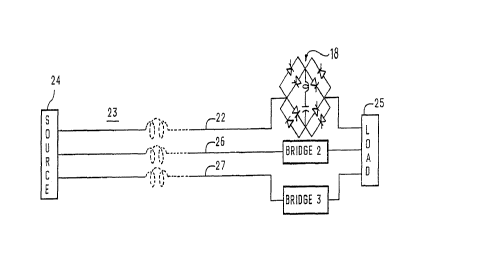
Referring to Figure 2, a thyristor bridge 18 is .
shown schematically having thyristors 10, 11, 12, 13, 14, ~
15, 16 and 17 connected in anti-parallel pairs as shown.
Connected across the bridge is a capacitor 20 in series
with a small surge-limiting inductor 21. As shown in
Figure 3, the bridge 18 may be connected in series in a
conductor 22 of a transmission line 23 which extends
between a source 24 and a load 25. The transmission line
23 also has conductors 26 and 27 with a respective bridge
2 and 3 similar to bridge 18. The system has a
predetermined operating frequency or supply frequency
which may, for example, be 50 ~Iz.. Thus, Figure 3 shows a
three phase transmission line 23 extending between a
source 24 (such as a generator or a plurality of
:J ~. '. ~ ._ > J t . r
- 7 - GECAN3044
generators, for example) and a load 25, with a respective
bridge in each conductor of the transmission line for
introducing a controlled amount of capacitive reactance
to compensate for or to partly compensate for the
inherent inductive reactance in the transmission line.
With reference now to Figures 2 and 4, it will be
seen that, for the purpose of switching the capacitor 20
into a series path and for by-passing capacitor 20, it is
not necessary to use the thyristors 12, 13 and 16, 17 of
Figure 2. Therefore the bridge 18 may be simplified, for
the purpose of describing the invention in its simplest
form, as shown in Figure 4 as bridge 1.8A. It is the
bridge 18A, or partial bridge 18A, or circuit arrangement
18A, that will form the basis of the following
description.
Referring now to Figures 4 and 5, there is shown in
Figure 5A a voltage waveform 30 which has the first cycle
beginning at time t0 and going to time tg. Also shown,
in broken line, is a current wavefarm 31 (system current)
which leads the voltage waveform 30 by 90 degrees. The
waveform 30 may represent the voltage across the
capacitor 20, and 'the waveform 31 may represent the
current through capacitor 20, with thyristors 10 and 11
in the conducting state or condition (i.e. switched on)
and thyristors 14 and 15 in the non-conducting state or
condition. Suppose now that at time t1 thyristor 14 is
switched on. Current flows out of capacitor 20 and
commutates off the thyristor 10. Thyristors 11 and 15
remain in the non-conducting state. Then the voltage
across capacitor 20 will no longer increase. In fact
there will be a small decrease due to the commutating
flow out of the capacitor. The voltage across capacitor
20 is represented by wave form 34 in Figure 5B, and it
will be seen that the voltage is substantially constant
i-J ,J ~.'. ,i t~ ,'
° 8 - GECAN3044
from time t1 to time t2 (the small decrease in voltage is
neglected for simplicity of drawing). The current
flowing through thyristor 14 by-passes capacitor 20 and
is represented by wavefarm 35 (Figure 5n), and this is
for the interval of time from t1 to t2. At time t2 the
thyristor 15 is switched on arid thyristor 14 turns off at
current zero. Current flows through thyristor 15 from
time t2 to time t3 as shown by that portion of waveform
35. At time t3 thyristor 11 is s~,aitched on and thyristor
15 is commutated to a non-conducting state by capacitor
current. From time t3 to time t5 the current flow
through capacitor 20 is represented by that portion of
waveform 36 (Figure 5C). At time t5 thyristor 15 is
switched on and thyristor 11 is commutated off. At time
t5 thyristor 14 is switched on and thyristor 15 is
commutated off. At time t7 thyristor 10 is switched on
and thyristor 14 is commutated off. It is believed that
the switching sequence fox the remainder of the waveforms
of Figure 5 will be apparent. The waveforms of Figure 5
represent a steady state condition, that is, a condition
where there are no changes taking place.
~, Referring now to Figure 4 and to the waveforms of
Figure 6 which represent a start-up situation, waveform
37 (Figure 6A) represents the voltage across capacitor
20. Waveform 38, shown by a dotted line, represents the
potential voltage waveform which would appear across a
conventional series capacitor of equivalent size caused
by the flow of system current. At time tl, when waveform
38 is at a maximum, thyristor 11 is switched on and the
others are non-conducting. The charge on capacitor 20
begins to build up (negatively). Current begins to flow
into capacitor 20 as shown by wavefarm 40 (Figure 6B)
following time tl. At time t2 when the voltage waveform
38 is passing through zero, thyristor 15 is switched on
K r :1 .a ~,. ;'a '~
i r : ;;
:,a ;i '.': ... G~ :', sa
- 9 - GECAN3044
and thyristor 11 becomes non-conducting. Waveform 41
(Figure 6C) beginning at time t2 shows current flow
by-passing capacitor 20. At time t3 thyristor 10 is
switched on and thyristor 15 is commutated off. Current
flows positively into capacitor 20 as shown by waveform
40. At time t5 thyristor 14 is switched on and thyristor
is commutated off. The voltage across capacitor 20
remains substantially constant from time t5 until time t7
as shown by waveform 37. At time t6 thyristor 15 is
switched on and thyristor 14 is commutated off. At time
t7 thyristor 11 is switched on and 15 is commutated off.
The capacitor compensation circuit arrangement 18A is now
in a running or steady state condition as described in
connection with Figure 5.
The capacitor compensation circuit arrangement 18A
must, of course, be able to change the effective
capacitance and this will be described with reference to
Figure 7.
Referring now to Figures 4 and 7, a waveform 42
(Figure 7A) shows the voltage across capacitor 20 under
various conditions, and waveforms 43 and 44 (Figure 7B
antd 7C respectively) show current through capacitor 20
and current which by-passes capacitor 20.
At time t0 a normal or steady state cycle begins as
represented by waveform 42 from t0 to tl. During this
interval thyristor 10 is conducting and the other
thyristors are non~conducting. At time tl thyristor 14
is switched on and thyristor 10 is commutated off. The
voltage across capacitor 20 no longer increases because
capacitor 20 is effectively out of the circuit. This can
be seen from waveform 42 (Figure 7A).
At times t2 thyristor 15 is switched on and
thyristor 14 commutates off. The current during the
ri
'J ~. ~ , ~.. : J F J
- GECAN3044
interval ti to t3 by-passes capacitor 20 as can be seen
from waveform 44 over this interval.
At time t3 thyristor 11 is switched on and
thyrist or 15 is commutated off. The voltage across
capacitor 20 begins to fall due to the flow of system
current (see waveform 43).
At time t4 the voltage across capacitor 20 passes
through zero (see waveform 42). A short time after this,
at time t5 far example, thyristor 15 is switched on and
thyristor a.i commutates off. Current begins to flow
through thyristor 15, by-passing capacitor 20 (see
waveform 44 from t5 to t6). At time t6 thyristor 14 is
switched on and thyristor 15 is commutated off. Current
continues to by-pass capacitor 20. Thus, from time t5 to
t~ capacitor 20 is effectively out of the circuit, and
the. voltage across capacitor 20 is quite small
(negatively).
At time t? which is close to the end of the first
voltage cycle, thyristor 10 is switched on and thyristor
14 is commutated off. Current flows through capacitor 20
for a short time interval from time t~ to tg when
thyristor 14 is again switched on and thyristor 10
commutates off. Tt will be seen that the time interval
represented by t~ to tg is relatively short. This
represents capacitive current flow (waveform 43 Figure
7B) .
Thyristor 14 is switched on from time tg to ti0 and
thyristor 15 is switched on from time ti0 to tii. At
time tii thyristor 11 is switched on and thyristor 15 is
commutated off. Current flows through thyristor 11 and
capacitor 20 until time t13.
As before, from time t13 to t14 thyristor 15
conducts and from time t14 to t15 thyristor 14 conducts.
f~~ ~ :/ ~ r, :~.I ~
w :J !..: "I~_ v ~ ' yV'
' fe
- 11 - GECAN3044
The voltage across capacitor 20 will remain substantially
constant during this interval as seen from waveform 42.
From time t15 to t17 thyristor 10 is switched on and the
others are non-conducting. Figure 6B shows the waveform
43 representing the current through the capacitor 20. It
will be seen that turning thyristor 10 on closer to time
t14 and having it non-conducting closer to time t1g will
result in a longer interval when current flows through
capacitor 20. Similarly, during the negative portion, if
thyristor 11 were turned on closer to time t10 and became
non-conducting closer to time t14 then current would flow
through capacitor 20 for a longer time interval. In this
manner the capacitive current can be controlled.
Referring now to Figure 8, 'there is shown a
simplified schematic drawing of a high voltage
transmission system incorporating the controlled
capacitive compensation arrangement of this invention. A
source 24 and a load 25 are shown as before. The
transmission line 23 is represented by a single conductor
45. Two capacitors 46 and 47 (which represent capacitor
banks) are connected in series in conductor 45, and
anti-parallel thyristor switches 50 and 51 are connected
in parallel with a respective capacitor 46 and 47. In
series with capacitors 46 and 47 is a partial bridge
circuit or capacitive compensation circuit arrangement
18A according to the invention. The capacitors 46 and 47
can be by-passed or left in series in the conductor 45 as
required. The amount of capacitive impedance can be
increased by using one or both of capacitors 46 and 47 in
addition to the capacitive compensating circuit
arrangement 18A. Thus the capacitive impedance can be
smoothly and rapidly increased and decreased by using
circuit arrangement 18A and adding capacitors 46 and 47
when needed.
Ci . f ,.~ ....n :,5
... f.~ '.l ~.'. '~~.. !/ ~.' i J
- 12 - GECAN3044
Referring now to Figure 9, there is shown an AC
source 24 and an AC load 25, as before. A bus 55 having
an AC voltage V1 represents the beginning of transmission
line conductor 23. Inserted in transmission line 23 is a
capacitor 46, representing a capacitor bank, that may be
switched into the transmission line 23 or may be
by-passed by anti-parallel thyristor switches 50. There
may, of course, be more than one bank of capacitors (for
example, capacitors 46 and 47, Figure 8). Also in series
with transmission line 23 is a capacitive compensation
circa it arrangement 18A. The control electrodes of
thyristors 50 are connected by conductors 56 to a firing
pulse distributor 57. The control. electrodes of the
thyristors in capacitive compensation circuit arrangement
18A are connected by conductors 58 to firing pulse
distributor 57. The transmission line 23 terminates at a
bus 60 at load end 25. The voltage on bus 60 is V2.
A potential transformer 61 is connected to bus 55
and applies a signal representing voltage V1 to a phase
angle detector circuit 62 over conductor 63. A potential
transformer 64 is connected to bus 60 and applies a
signal representing V2 to a communications device 65 over
conductor 66. The communications device 65 may represent
a radio link, a wire link or the like, and a path 67
connects the device 65 to a phase angle detector circuit
62 to apply thereto a signal representing V2. The phase
angle detector circuit 62 derives a signal representing
the phase angle between V1 and V2, that is, the angle
referred to as delta, and it provides this signal on
conductor 68 to an adder 70. Also applied to adder 70,
over conductor 71, is an angle reference signal. The
resulting difference signal on conductor 72 is applied to
a regulator 73 which may limit or regulate amplitude or
rate of change. The resulting signal on conductor 74 is
,;~,:3
,. ;i
13 - GECAN3044
applied to a firing sequence logic circuit 75. Also
applied to the firing sequence logic circuit 75 is a
signal representing V1 from conductor 63, and a signal
representing VC, the voltage across capacitance 20 (see
also Figures 2 and 4). The signal representing VC is
determined direc4ly from capacitance 20 in the capacitive
compensating circuit arrangement 18A and provided via
conductor 76, The output from firing sequence logic
circuit 75 is provided over conductor 77 to a firing
pulse generator 78 whl.Ch, in turn, provides signals on
conductor 80 to the firing pulse distributor 57. The
firing pulse distributor 57 provides appropriate signals
on conductors 56 and 58 to gate on desired thyristors at'
desired times as was explained with reference to the
waveforms of Figures 5, 6 and 7.
It should be understood that any or all of the
conductors used to transmit signals or gate thyristors
may be in practise replaced by light fibers.
Because the angle delta, the reactance and the
power transmitted are related, it is possible to use
detectors other than the phase angle detector 62. For
example, a power transducer having as inputs system
current and voltage signals could provide a suitable
signal to adder 70. The reference signal on conductor
71, in this case, would be a power reference signal.
However, the signal provided to regulator 73 would be
quite suitable for deriving a firing sequence signal to
effect a satisfactory control.
The thyristors can be gated on quickly and
precisely to provide rapid, simple arid accurate amounts
of capacitive compensation in a transmission system. Not
only can the net reactance be controlled but the response
is sufficiently rapid to provide damping for undesired
oscillations which might occur in a power transmission
system.