Note: Descriptions are shown in the official language in which they were submitted.
;~0~3~9
TITLE OF THE INVENTION
MULTIPAT~I TRANSMISSI~N SYSTEM
B~CKCROUND OF T~E INVENTION
Field of the Invention
This invention relates to a multipath transmission
system for transmitting data among multiplex nodes
connected to common signal transmission lines.
Descrlption of the Related Ar-t
This type of multipath transmission system
includes a transmission system of LAN (Local Area
Network) utilizin~ a CSMA/CD (Carrier Senser Multiple
Access/Collision Detection) with an NDA (Non
Destructive Arbitration). A typical example of -the LAN
is a CAN (Controller Area Network) used for data
transmission in cars, for example.
In the multipath transmission system utilizing the
CAN, terminal resistors R~, R~ are connected to both
ends of two signal transmission lines A and B and a
plurality of multiplex nodes are connected in parallel
with the signal transmission lines A and B.
Each of the multiplex nodes is constructed by a
communication con-trol device, a transmission circuit
for receiving a transmission signal from the
communication control device and transmitting the same
to the signal transmission line, and a reception
circuit for receiving a signal from the signal
transmission line and transmitting the same to the
communication control device.
The reception circuit outputs a signal received
from the signal transmission line to a comparator of
the communication control device. An adequate
Z(l ~3~
-- 2
threshold voltage is applied to the comparator to
reduce the amplitude of the transmission signal to a
permiss:Lble level so that the range o-f an input voltage
ln the common mode of the reception circuit can be
widen and in-r:luence by noises can be reduced.
The transmission circuit includes two -field ef-fect
transistors (FET) and the FETs are connected to the
signal transmission lines.
Therefore, when the multiplex nodes are set in the
passive state, that is, when a recessive bit is output
in the transmission system o-f ~CSMA/CD+NDA), each FET
is set in the ~FF state, no potential di-f-ference occurs
between the signal transmission lines and a high
impedance state is set the output terminal. Further,
when the multiplex nodes are set in the dominant state,
that is, when a dominant bit is output in the
transmission system o-f (CSMA/CD+NDA), each FET is set
in the ON state, a current is supplied to one of the
transmission lines and a current is drawn -from the
other signal transmission line. There-fore, in the
dominant state, a potential di-fference occurs between
the signal transmission lines and the reception circuit
corinected to the signal transmission line detects the
potential di-f-ference and converts this signal in order
to recognize the signal ~ace. As a result, the
communication control device can detect the dominant
state.
With the above transmission system, when an
accident such as an open circui-t or short circuit
occurs in one o-P the signal transmission lines, for
example, and thus when -fault occurs in the transmission
system, a potential between the signal transmission
lines is changed ~rom a transmissible value so that a
signal cannot be correctly transmitted between all o-f
- 3 - 2~3~
the multiplex nodes associated with the signal
transmission line.
SUMM~RY OF T~E INVEN~ION
This invention has been made in view o-f the above
problem, and an object o-f this invention is to provide
a multipath transmission system which permits data to
be e-f-ficiently and reliably transmitted among multiplex
nodes even when fault occurs in the signal transmission
line and which can be preferably applied to cars.
The above object can be attained by a multipath
transmission system o-f this invention and the multipath
transmission system comprises:
at least three common signal transmission lines;
a plurality o-f multiplex nodes connected in
parallel to the signal transmission lines, each o-f the
multiplex nodes including a transmission circuit which
is allotted to a corresponding device, receives a
multiplex signal -from a corresponding device in
response to a transmission request o-f another multiplex
node, and transmitting the multiplex signal to the
transmission line;
voltage detection means for detecting a voltage
occurring in at least one o-f the signal transmission
lines;
speci-fyi.ng means for speci-fying the transmission
state of each of -the signal transmission lines
according to the voltage detected by the voltage
detecting means;
fault detecting means -for communicating with each
o-f the multiplex nodes to detect fault; and
voltage changing means for changing a voltage of
the signal transmission line when fault is detected by
-the fault detecting means.
- 4 ~ 3~9
According to the multipath transmission system,
three or more signal transmission lines are used and
each multiplex node detects a voltage o-f at least one
o-f the signal transmission lines, speci-fies the
transmission state o-f each o-f the signal transmission
lines according to the detected voltage, and if at
least one of the multiplex nodes communicates with each
of the multiplex nodes to detect fault, a preset
potential difference is caused between the signal
transmission lines by changing the voltage o-f the
signal transmission line 90 as to change the state o-f
each of the signal transmission lines into the signal
transmissible state, and there-fore, a signal can be
transmitted among the multiplex nodes even when fault
occurs in the transmission line, thereby enhancing the
reliability o-f the signal transmission and the
transmission e-fficiency.
The a-forementioned obJects, -features and
advantages o-f this invention will become more apparent
in the following detailed description made with
reference to the accompanying drawings.
BRIEF DESCRIPTION OF TIIE DRAWINGS
Fig. 1 is a diagram showing the layout of a
multipath transmission system incorporated into a car
and is a constructional block diagram showing the
construction of a multipath transmission system
according to this invention;
Fig. 2 is a constructional block diagram showing a
first embodiment of the multlpath transmission system
shown in Fig. 1;
Fig. 3 is a constructional block diagram showing a
second em~odiment of the multipath transmission system
shown in Fig. 1;
- 5 - 2~4~3~9
Fig. 4 is a constructional block diagram showing a
third embodiment o-f the multipath transmission system
shown in Fig. 1;
Fig. 5 is a circuit diagram showing one embodiment
of a voltage detection circuit shown in Fig. 1;
Fig. 6 is a circuit diagram showing one embodiment
of a transmission control circuit shown in Fig. 1;
Fig. 7 is a circuit diagram showing one embodiment
o-f a reception control circuit shown in Fig. 1;
Fig. 8 is a circuit diagram showing one embodiment
of a terminal circuit shown in Fig. 1;
Fig. 9 is a flowchart for i~lustrating the
operation of the fault correction effected for the
slgnal transmission line by a multiplex node shown in
Fig. 1;
Fig. 10 :Ls a diagram showing a potential in the
normal transmission state;
Fig. 11 is a diagram showing a potential in the
abnormal transmission state;
Fig. 12 is a diagram showing a potential in the
abnormal transmission state;
Fig. 13 is a diagram showing another embodiment of
the reception contro] circuit; and
Fig. 14 is a constructional diagram showing a
-fourth embodiment o-f the multiplex node.
DESCRIPTION OF T~E PBEFERRED EMBODIMENTS
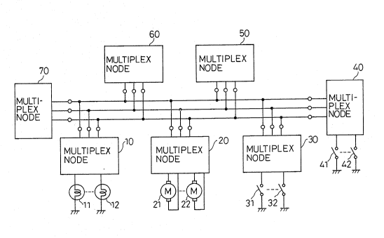
Referring to Fig. 1, a multipath transmission
system is incorporated in a car. The multipath
transmission system includes a plurality of multiplex
nodes, for example, multiplex nodes 10 to 70 and signal
transmission lines A, B and C. The multiplex nodes 10
to 70 are connected in parallel to the three signal
transmission lines A, B and C. The multiplex nodes 10
- 6 - ~ 3~
to 70 transmit data signals via the signal transmission
lines A, B and C. For example, among the multip:Lex
nodes 10 to 70, the mul-tiplex node 10 is connected with
a headlight 11 and a turn signal light 12, the
multiplex node 20 is connected with a door lock motor
21 and a door unlock motor 22, the multiplex node 30 is
connected with a headlight switch 31 and a turn signal
switch 32, and the multiplex node 40 is connected with
a door lock switch 41 and a door un].ock switch 42.
The multiplex node 10 turns on or o-f-f the
headlight 11 and the turn signal light 12 in response
to signals o-E the headlight switch 31 and the turn
signal switch 32 transmitted -from the multiplex node
30.
The multiplex node 20 drives the door lock motor
21 and door unlock motor 22 in response to signals o-f
the door lock switch 41 and door unlock switch 42
transmitted from the multiplex node 40.
Further, the multiplex node 50 controls an air
conditioner (not shown) in the car, the multiplex node
60 controls an operation switch (not shown) o-f the air
conditioner, and various signals for controlling the
air conditioner are transmitted between the multiplex
nodes 50 and 60. The multiplex node 70 is connected
with various indicators (not shown).
Fig. 2 is a diagram concretely showing the
multiplex node 10 o-f the multipath transmission system
shown in Fig. 1. The construction of the multiplex
nodes 20, 30, 50 and 60 is the same as that o-E the
multiplex node 10, and the construction o-f the
multiplex node 10 is explained as an example here for
convenient explanation.
Referring to the first embodiment shown in Fig. 2,
the multiplex node 10 includes a communication control
- 7 - ~ ~4~3~9
device 11 -for ef-fecting the communication process
control, a transmission control circuit 12 for
receiving a transmission signal -from the communication
control device 11 and transmitting the same to the
signal transmission lines A, B and C, a reception
control circuit 13 for supplying reception signals
received from the signal transmission lines A, B and C
to the communication control device 11, and a voltage
detection circuit 14 -for detecting a voltage of one o-f
the signal transmission lines.
The communication control device 11 effects the
communication process control for receiving an output
signal from the device connected thereto, constructing
the output signal in a frame config-uration for each
preset data unit, and transmitting the signal formed in
the frame configuration as a transmission signal to the
transmission control circuit 12. Further, the
communication control device 11 e-ffects the
communication process control for receiving a reception
signal formed in the -frame configuration from the
reception control circuit 13, deriving only a signal
necessary therefor from the reception signal, transmits
the signal to the device connected thereto, and
transmitting a acknowledge signal (ACK signal) to the
transmission control circuit 12 when the signal
reception is correctly effected.
The transmission control circuit 12 is connected
to the multiple transmission l:Lnes A, B and C, converts
a transmission signal (including the ACK signal) -from
the communication control device 11 transmits the same
to the multiple transmlssion lines A, B and C.
The reception control circuit 13 is connected to
the multiple transmission lines A, B and C, and when
receiving a reception signal (including the ACK signal)
2~3~
-- 8
-from the multiple transmission lines A, B and C, it
outputs the reception signal to the communication
control device 11.
The voltage detection circuit 14 is connected to
one o-f the transmission lines, -for example, the
transmission line C, the communication control device
11, the transmission control circuit 12 and the
reception control circuit 13, and it detects a voltage
o-f the transmission line C and in-forms the
communication control device 11, the transmission
control circuit lZ and the reception control circuit 13
o-f the state of the transmission line C.
Re-~erring to a second embodiment shown in Fig. 3,
a multiplex node 40 connected to the terminal ends o:~
signal transmission lines A, B and C includes a
communication control device 41, a -transmission control
circuit 42, a reception control circuit 43 and a
voltage detection circuit 44 having the same function
as the multiplex node 10 and further includes a
terminal circuit 45 having terminal resistors connected
to both ends of the transmission lines A, B and C.
Referring to a third embodiment shown in Fig. 4, a
multiplex node 70 connected to the terminal ends
includes a communication control device 71, a
transmission control circuit 72, a reception control
circuit 73, a voltage detection circuit 74 and a
terminal resistor 75 having the same function as the
multiplex node 40 and -further includes a voltage
generation circuit 76 -for applying a voltage to the
signal transmission line C.
The concrete construction o-f each o-f the voltage
detection circuits is shown in Fig. 5. Re-ferring to
Fig. 5, the one terminal o-f a voltage comparator
circuit CM1 and the one terminal o-f a voltage
Z~ 3~9
g
comparator circuit CM2 are applied with a voltage VO Oe
the transmission line C via a -filter circuit -formed o-f
a resistor R1o and a capacitor C1o. The other terminal
of the voltage comparator circuit CM1 and the other
terminal Oe the voltage comparator circuit CM2 are
applied with reference voltages Vl and V2 which are
obtained by dividing a power source voltage Vcc by
resistors R11 to R13. As a result, the voltage
comparator circuits CMl and CM2 check whether or not
the voltage VO o-f the transmission line C is within the
range of the reference voltages V1 and V2 by comparing
the voltages applied to both o-f the terminals. That
ls, when the vol-tage VO is within the range of the
re-ference vo]tages V1 and V2, the voltage comparator
circuits CM1 and CMz output "O" and "O" indicating the
normal state to output terminals K1 and K2. When the
voltage VO exceeds the range o-f the reference voltages
V1 and V2, -for example, when the transmission line B is
broken on the ground, the voltage comparator circuits
CM1 and CM2 output "O" and "1" indicating the abnormal
state to the output terminals K1 and K2. When the
voltage VO exceeds the range of the reference voltages
V1 and V2, -for example, when failure occurs anywhere in
the voltage detecion circuits and the transmission line
C was set at 5 voltages, the voltage comparator
circuits CM1 and CMz output "1" and "O" indicating the
abnormal state to the output terminals K1 and K2.
The concrete circuit construction o-f each of the
transmission control circuits is shown in Fig. 6.
Re-ferring to Fig. 6, the drain terminals of FET1 and
FET2 are connected to filter circu:Lts formed of diodes
D1o and D1l and resistors R1~ and R1~. The FET1 is
connected to a filter circuit formed o-f a diode D1o and
the resis-tor R1~ to the transmission line A. The FET2
~ 4~3~
-- 10 --
is connected to a -filter circuit -formed of a diode Dll
and the resistor Rl~ to the transmission line B. That
is, when the multiplex node is set in the passive
state, each FET is set in the OFF state so that no
potential di-fference may occur between the signal
transmission lines A and B and a high impedance state
may occur the output terminals. Further, when the
multiplex node is set in the dominan-t state, each FET
is set in the ON state, causing a current to flow into
the signal transmission line A and receiving a current
-from the other transmission line B. There-fore, in the
dominant state, a potential occurs between the signal
transmission lines A and B and the reception circuit
connected to the signal transmission lines A and B
detects the potential di-fference. As a result, the
communication control device can detect the dominant
state.
The concrete construction o-f each reception
control circuit is shown in Fig. 7. Referring to Fig.
7, a power source voltage 1/2 Vcc is applied to the
signal transmission lines A, B and C via resistors Rl~,
Rl7 and Rl8. One-side ends o-f the signal transmission
lines A, B and C are connected to the input terminals
of a voltage comparator CM3 via switching elements Sl
to S~ shown in the drawing. The ON/OFF states o-f the
switching elements Sl to S~ are controlled by the
voltage detection circuit, and the voltage detection
circuit controls the ON/OFF states o-f the switching
elements Sl to S~ in response to signals input -from the
output terminals Kl and K2 according to combinations
shown in the -following first table. Resistors Rl~ to
R23 are resistors for voltage division and setting o-f
the threshold voltage.
~O~L~3~9
FIRST TABL~
Kl K2 Sl S2 S3 S~
O O ON OFF OFF ON
1 O ON OFF ON OFF
O 1 OFF ON OFF ON .
Further, the reception control circuit transmits
signals in the balanced transmitting condition set by
using the positive logic -for the signal transmission
line A and the negative logic for the signal
transmission line B in the normal state in which
outputs o-~ the output terminals Kl and K2 are "O" and
"O". That is, the signal reception is e-f-fected by
settlng the signal transmission line A in the dominant
state when a voltage is high and setting the signal
transmission line B in the dominant state when a
voltage is low. Further, the reception control circuit
receives signals in the unbalanced transmitting
condition set by using the signal transmission line C
as a -fixed potential line and the negative logic -for
the signal transmission line B in the abnormal state in
which outputs o-f the output terminals Kl and K2 are "1"
and i.o.. and receives signals in the unbalanced
transmitting condition set by using the signal
transmission line C as a fixed potential line and the
positlve ]ogic for the signal transmission line A in
the abnormal state in which outputs of the output
terminals Kl and K2 are "O" and "1". Since high
-frequency components o-f the transmission wave are
little contained in the signal transmission line C
under the normal transmission state and the signal
transmission lines A and B surrounded by the signal
2~3Q19
- 12 -
transmission llne C can be used, the cost of the signal
transmission line can be reduced equivalent to that o~
the conventional two-core shield line.
The concrete circuit construction of the terminal
circuit 45 is shown in Fig. 8. Re-ferring to Fig. 8, a
resistor R~ connected between the ends of the signal
transmission lines A and B is divided into two portions
o-f R~/2 by the signal transmission line C, and the
signal transmission line C is connected to switching
elements S~ and S~ via a resistor R2~. The resistance
of the resistor R2~ is relatively smaller than -that O-e
the terminal resistor. The switching element S~ is
constructed to be turned on when an ou-tput SKl -from the
communication control device is "1" and the switching
element S~ is constructed to be turned on when an
output SK2 -from the communication control device is
"1". Further, the terminal circuit 45 is also used
instead o-f the voltage generation circuit 76 -for the
signal transmission line C, and when it is required to
forcedly set outputs o-f the output terminals Kl and K2
to "1" and "O" in the multiplex node 70, -for example,
the switching element S~ is turned on by the control o-f
the communication control device 71. When it is
required to -forcedly set outputs o-f the output
terminals K1 and K2 to "O" and "1", the switching
elemen-t S~ is turned on by the control of the
communication control device 71.
In this embodiment, the terminal circuit 45 and
the voltage generation circuit 76 which can control the
voltage in the signal transmission line C are included
in a system. So -Ear as controlling o-f each other
concerned. Output terminals SKl and SK2 o-f terminal
circuit 45 and that of the voltage generation circuit
76 are operated each other by synchronization, or are
3~i9
respectively used as main or sub.
Next, the operation o-f the -fault correction with
respect to the signal transmission line by the
multiplex node 70 is explained with reference to the
-flowchart shown in Fig. ~. II1 this case, the outputs
o-f the output terminals K1 and Kz o-f the voltage
detection circuit 54 are set to the normal state o-f "O"
and "O" and the switching elements S1 and S~ among the
switching elements S1 to S~ are set shown in Fig. 7 in
the ON state and are set the switching elements S2 and
S3 in the OFF state.
First, the communication control device 71 can
check whether the signal transmission can be e-f-eected
or not according to whether each multiplex node, -for
example, the multiplex node 30 -for the multiplex node
10 or the multiplex node 40 for the multiplex node 20
can correctly transmit -frames or not when the frame of
the transmiss:ion signal is received (step 101).
Next, whether communication with all of the
multiplex nodes is possible or not is checked by
determining the reception o-f an ACK signal from all o-f
the multiplex nodes in the same manner as described
above (step 102). In this case, i-f it is determined
that -the communication is possible, the normal s-tate in
which the outputs SK1 and SKz from the communication
control device are set at "O" and "O" is maintained
(step 103) and the checking operation in the step 101
is effected again.
Further, when it is determined in the step 101
that the transmission is impossible, or when it is
determined in the step 102 that communication with all
o-f the multiplex nodes is impossible, the output
terminal SK1 and SKz of communication control device 71
are set at the output state O-e ~ and "O"(step 104),
3~g
- lA -
therefore the output state o-f the output terminals K
and K2 are set the state o-f "1" and "O" and the
swi-tching elements Sl and S3 among the switching
elements S1 to S4 of the reception control circuit 73
shown in Fig. 7 are set in the ON state and the
switching elements Sz and S4 are set in the OFF state.
Then, whether transmission with respect to the
reception multiplex node is possible or not is checked
in the same manner as :Ln the step 101 (step 105).
In this case, if the transmission with respect to
the reception multiplex node is possible, then whether
communication with all o-f the multiplex nodes is
possible or not is checked in the same manner as in the
step 10~ (step 106). In this case, i-f the
communication is poss:Lble, the outputs o-f the output
terminals SK1 and SKa are kept at the output state o-f
"1" and "O" (step 107) and then the determination in
the step 105 is e-f-fected again.
I-f it is detected in the step 105 that the
transmission is impossible, or when it is determined in
the step 106 that communication with all o-f the
multiplex nodes is impossible, the switching elements
S~ and S~ of the voltage generating circuit 76 are
respectively -forcedly turned off and on to change the
output state of the output terminals Kl and K2 of
voltage detecting circuit 7A to the state o-f "O" and
"1" (step 108). And the switching elements S1 and S~
among the switching elements Sl to S~ of the reception
control circuit 73 shown in Fig. 7 are set in the OFF
state and the switching elements Sz and S4 are set in
the ON state. Then, whether transmission with respect
to the reception multiplex node is possible or not is
checked in the same manner as in the step 101 (step
109).
- 15 - 20~3~9
In this case, if the transmission with respect to
the reception multiplex node is possible, then whether
communicati.on with all o-f the multiplex nodes is
possible or not is checked in the same manner as in the
step 102 (step 110). In this case, if the
communication is possible, the outputs SK1 and SK2 -from
the communication control device are kept in the output
state of "0" and "1" (step 111) and then the
determination in the step 109 is ef-fected again.
I-f it is detected in the step 109 that the
transmission is impossible, or when it is determined in
the step 110 that communication with all of the
multiplex nodes is impossible, it is determined that
the -fau]t is not in the transmission line and the
switching elements S~ and S~ o-f the voltage generation
circuit 76 are -forcedly set in the OFF state to return
the OUtpllt state of the output terminals K1 and Kz to
the state o-f "0" and "0" (step 112). Then, the
operation for the other -faul-t correction routine is
e-f-fected (step 113).
Therefore, in a case where the state o-f the
outputs from the output terminals K1 and K2 is set in
the normal state o-f "0" and "0" in the multiplex node
70, a potential dif-ference occurs between the signal
transmission lines A and B in the dominant state as
shown in Fig. 10. As a result, the reception control
circuit 73 connected to the signal transmission lines A
and B detects the potential di-f-ference and the
communication control circuit 71 can detect the
dominant state. Further, in a case where one o-f the
signal transmission lines is -fixed at a constant
voltage, where one o-f the signal transmission lines is
broken, or where two o-f the signal transmission lines
are shor~t-circuited to each other, the output terminals
Z6~4~3~9
- 16 -
SK1 and SK2 are set to the state of "1" and "0", so
that the switching elements S1 and S3 among the
switching elements Sl to S~ o-f the reception control
circuit 73 shown in Fig. 7 can be se-t in the ON state
and the switching elements S2 and S~ can be set in the
OFF state. If the transmission is possible in this
state, a potential occurs between the signal
transmission lines C and B in the dominant state as
shown in Fig. 11. As a result, the reception control
circuit 73 connected to the signal transmission l:Lnes C
and B detects the potential difference and the
communication control circuit 51 can detect the
dominant state. In this case, the potential of the
transmission line A may be -rreely set.
Further, in another case, the output terminals SK
and SK2 are changed to the state o-f "O" and "1" when
the transmission is impossible so that the switching
elements S1 and S~ among the switching elements S1 to
S~ o-f the reception control circuit 73 shown in Fig. 7
can be set in the OFF state and the switching elements
S2 and S~ can be set in the ON state. If the
transmission is possible in this state, a potential
occurs between the signal transmission lines A and C in
the dominant state as shown in Fig. 12. As a result,
the reception control circuit 73 connected to the
signal transmission lines A and C detects the potenti.al
dif-ference and the communication control device 71 can
detect the dominant state. In this case, the potential
of the transmission line B may be freely set.
~ s described above, according to the multipath
transmission system of this invention, even when an
accident such as breakage or short-circuit occurs in
the signal transmission line, a preset potential occurs
between the signal transmission lines so as to permit
2~4~3~:39
- 17 -
the signal transmission between the multiplex nodes,
thereby maklng i-t possible to enhance the reliability
of the multiplex transmission of the whole system.
This invention is not llmited to the multipath
transmission system of the above embodiment. Referring
to Fig. 13, the reception control circuit includes
three voltage comparator circuits CM4 -to CM~ and a
select circuit SE connected to the output terminals of
the voltage comparator circuits CM4 to CM~. A power
source voltage 1/2 Vcc is applied to the transmission
lines A, B and C via resistors R2~, R2~ and R27 in the
same manner as shown in Fig. 7. One-side ends of the
transmission lines A, B and C and the input terminals
of the voltage comparator circuits CM~ to CM~ are
connected as shown in the drawing.
The select circuit SE receives output signals
(potential di-fference) -from the voltage comparator
circui-ts CM4 to CM~. The select circuit SE selects the
received output signal according to the outputs of the
output terminals Kl and K2. That is, the select
circuit SE selects the output signal from the voltage
comparator circuit CM4 when Xl = K2 = O, selects the
output signal -from the voltage comparator circuit CMG
when Kl = 1, and selects the output signal from the
voltage comparator circuit CM~ when K2 = 1, and then
transmits the selected signal to the communication
control device. In this case, a plurality of switching
elements shown in Fig. 7 are not necessary, thus making
it possible to reduce the number of parts used.
- Further, another concrete circuit construction of
the multiplex node is shown in Fig. 14. Referring to
the fifth embodiment shown in Fig. 14, the
communication control device 71 in the multiplex node
can detect the communication possible state of the
2~ 3~3
signal transmission lines -from the states of Kl = Kz =
O, K1 = 1, and K2 = 1. That is, the states of Kl and
Kz are output to the reception control circuit 73 to
select the output signal (potential dif-ference) -rrom
the voltage comparator circuit of the reception control
circuit 73 and detect the optimum transmission state
for the transmission -erom the transmission control
circuit 72. In this case, the number o~ parts used can
be reduced and a multiplex node having the above
voltage detection circuit and a multiplex node having
no voltage detection circuit can be disposed together.