Note: Descriptions are shown in the official language in which they were submitted.
20~135~
IMAGE DISPLAY APPARATUS
BACKGROUND OF THE INVENTION
Field of the Invention
This invention relates to an image display apparatus
provided with an automatic pedestal processing section for
detecting the minimum signal level of input video signals and
controlling the signal level of the video signals on the basis
of the detected results. The present invention may be applied
to, for example, an image display apparatus, such as a television
receiver having display means in the form of a display raster or
screen having a wide aspect ratio.
Description of the Prior Art
An image display apparatus, such as a television receiver,
adapted for displaying an image by image or video signals by
display means such as a Braun tube or liquid crystal display, has
been known widely. With such image display apparatus, an
automatic pedestal processing section for detecting the minimum
signal level of the input video signals and controlling the
signal level of the video signals on the basis of the detected
results is provided in the image signal processing system for
displaying an image with excellent picture quality by effective
exploitation of the dynamic range of the display means.
Meanwhile, with the present television broadcasting system,
the display screen has an aspect ratio of 4:3. In a second
generation extended definition TV (EDTV), scheduled to be
2041354
practiced in future, or a high quality television broadcasting
system, such as so-called high vision" broadcasting system, a
widescreen having an aspect ratio of 16:9 is scheduled.
Thus it is estimated that television broadcasting in future
will be made with both the presently adopted standard aspect
ratio of 4:3 and the wide aspect ratio of 16:9. For this reason,
development of an image display apparatus adapted for displaying
images of both types of the image signals is proceeding at
present.
In such image display apparatus, various display systems
such as shown in Figs. 1 to 4 are presently proposed as the
system for displaying the image of the video signals with the
standard aspect ratio of 4:3, using display means for the display
screen having a wide aspect ratio of 16:9, as an example.
In the first system, upper and lower regions Pl and P2 of an
image PN of image signals having a standard aspect ratio are cut
as shown in Fig. 1 to display an image P3 on the entire display
screen having a wide aspect ratio. With this first system, the
image is displayed on the display screen of the wide aspect ratio
by overscanning in the vertical direction of the screen without
meddling with the image signals of the standard aspect ratio.
In the second system, as shown in Fig. 2, a right-hand side
region AR of the display raster of the wide aspect ratio is
masked and the image PN of the image signals of the standard
aspect ratio is displayed in the left-hand side region of the
- - - - - - -
204135~
display raster of the standard aspect ratio. With the second
system, the image signals having the standard aspect ratio are
compressed along the time axis to three-fourths in the horizontal
direction in conformity to the difference in the aspect ratio
relative to the display raster of the wide aspect ratio. Frame
signals displaying the right-hand side region AR by, for example,
a black tint, are annexed, and the image display is made on the
display screen of the wide aspect ratio by usual raster scanning.
In the third system, shown in Fig. 3, left- and right-hand
side regions ALo and ARo of the display raster having the wide
aspect ratio are masked and the image PN of the image signals
having the standard aspect ratio is displayed at the center of
the display screen of the wide aspect ratio. With this third
system, image signals of the standard aspect ratio are compressed
along the time base to three-fourths in the horizontal direction,
in conformity to the difference in aspect ratio relative to the
display screen of the wide aspect ratio. Frame signals
associated with the left- and right-hand side regions Alo and ARo
are affixed and display is made on the display screen of the wide
aspect ratio by usual raster scanning.
In the fourth system, shown in Fig. 4, a left-hand side
region AL of the display screen having the wide aspect ratio is
masked, and the image PN of the image signals of the standard
aspect ratio is displayed on the right-hand side of the display
screen having the wide aspect ratio. With this fourth system,
- 20~13~
the image signals of the standard aspect ratio are compressed
along the time base to three-fourths in the horizontal direction,
in conformity to the difference in the aspect ratio relative to
the display screen of the wide aspect ratio. Masking signals
associated with the left-hand side region AL are affixed and
display is made on the display screen of the wide aspect ratio
by usual raster scanning.
Meanwhile, with the image display apparatus, adapted for
displaying the image of the wide aspect ratio and the image of
the standard aspect ratio by display means consisting of the
display screen having the wide aspect ratio, a problem is raised
in that, when an automatic pedestal processing section is
provided for improving the picture quality of the displayed
image, the masking signal having the signal level within the
range of level detection by the automatic pedestal processing
section is erroneously detected as being of the black level, so
that the automatic pedestal processing section is erroneously
actuated and hence it becomes impossible to make image display
in such a manner as to take advantage effectively of the dynamic
range of the display means.
Object and Summary of the Invention
The present invention has been made in view of the above
status of the art. A principal object of the present invention
is to provide an image display apparatus adapted for displaying
an image of the wide aspect ratio and an image of the standard
2U413~1
aspect ratio by display means consisting of the display screen
of the wide aspect ratio, in which mistaken actuation of the
automatic pedestal processing section may be prevented and an
image display may be made in such a manner as to take advantage
of the dynamic range of the display effectively.
According to the present invention, the automatic pedestal
processing section, controlled in operation by a control section,
is operated only during the effective display period for input
image signals so as to detect the minimum signal level of the
input image signals to control the signal level of the image
signals on the basis of the detected results. In this manner,
with the image display apparatus according to the present
invention, mistaken operations of the automatic pedestal
processing section due to detection of signals occurring during
the ineffective display period other than the effective display
period may be eliminated and the dynamic range of the display
means may be effectively exploited to enable image display with
the desired excellent picture quality.
BRIEF DESCRIPTION OF THE DRAWINGS
Fig. 1 is a schematic front view showing an image displayed
in the first system according to which upper and lower regions
of the image by the image signals with the standard aspect ratio
are cut and the image display is made on the overall display
screen having the wide aspect ratio.
Fig. 2 is a schematic front view showing an image displayed
2041354
in the second system according to which a right-hand side region
of the display screen having a wide aspect ratio is masked and
the image of the image signals with the standard aspect ratio is
displayed on the left-hand side region of the display screen
having the wide aspect ratio.
Fig. 3 is a schematic front view showing an image displayed
in the third system according to which left- and right-hand side
regions of the display screen having a wide aspect ratio are
masked and the image of the image signals with the standard
aspect ratio is displayed at the center of the display screen
having the wide aspect ratio.
Fig. 4 is a schematic front view showing an image displayed
in the fourth system according to which a left-hand side region
of the display screen having the wide aspect ratio is masked and
the image of the image signals with the standard aspect ratio is
displayed on the right-hand side region of the display screen
having the wide aspect ratio.
Fig. 5 is a block diagram showing an arrangement of an image
display apparatus according to the present invention.
Fig. 6 is a block diagram showing an arrangement of an
aspect ratio converting circuit of the image display apparatus
shown in Fig. 5.
Fig. 7 is a block diagram showing an arrangement of a write
clock generating circuit of the aspect ratio converting circuit
shown in Fig. 6.
204135~
_ .
Fig. 8 is a time chart for illustrating the operation of the
write clock generating circuit shown in Fig. 7.
Fig. 9 is a block diagram showing an arrangement of a
readout clock generating circuit of the aspect ratio converting
circuit shown in Fig. 6.
Fig. 10 is a time chart for illustrating the operation of
the readout clock generating circuit shown in Fig. 9.
Fig. 11 is a block diagram showing an arrangement of a line
memory of the aspect ratio converting circuit shown in Fig. 6.
Fig. 12 is a time chart for illustrating the operating of
data reading from the line memory shown in Fig. 11.
Fig. 13 is a block diagram showing an arrangement of a
countdown circuit of the aspect ratio converting circuit shown
in Fig. 6.
Fig. 14 is a time chart for illustrating the operation of
the countdown circuit shown in Fig. 13.
Fig. 15 is a time chart for illustrating the operation of
the aspect ratio converting circuit of Fig. 6 in each of the
display modes.
Fig. 16 is a schematic waveform diagram for explaining the
position of generation of a control signal used for actuating an
automatic pedestal processing circuit during the period of
effective display of the image signals in the display mode for
displaying the image on the overall display screen having the
wide aspect ratio by cutting upper and lower regions of the image
2~41354
-
of the image signals with the standard aspect ratio.
Fig. 17 is a schematic waveform diagram for explaining the
position of generation of a control signal used for actuating an
automatic pedestal processing circuit during the period of
effective display of the image signals in the display mode for
displaying the image of the image signals of the standard aspect
ratio on a left-hand region of the display screen of the wide
aspect ratio by making the right-hand side region of the display
screen with the wide aspect ratio.
Fig. 18 is a schematic waveform diagram for explaining the
position of occurrence of a control signal used for actuating an
automatic pedestal processing circuit during the period of
effective display of the image signals in the display mode for
displaying the image of the image signals with the standard
aspect ratio in the center of the display screen having the wide
aspect ratio by masking the left- and right-hand side regions of
the display screen having the wide aspect ratio.
Fig. 19 is a schematic waveform diagram for explaining the
position of occurrence of a control signal used for actuating an
automatic pedestal processing circuit during the period of
effective display of the image signals in the display mode for
displaying the image of the image signals with the standard
aspect ratio in the right-hand side region of the display screen
having the standard aspect ratio by masking the left-hand side
region of the display screen having the wide aspect ratio.
204135~
_,
Detailed Description of Preferred Embodiment
By referring to the drawings, an illustrative preferred
embodiment of the image display apparatus according to the
present invention will be explained in detail.
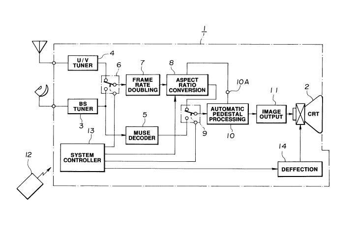
In an image display apparatus 1, shown in Fig. 5, the
present invention is applied to a high definition television
receiver displaying an image by a picture tube 2 having a display
raster of a wider aspect ratio of 16:9.
The image display apparatus 1 has a BS tuner circuit 3 for
transmitting and receiving signals of satellite broadcasting and
a U/V tuner circuit 4 for transmitting and receiving ground
waves.
The MUSE signals, obtained as the reception output by the
BS turner circuit 3 of the high definition broadcasting, are
supplied to a MUSE decoding circuit 5 and thereby decoded into
high quality video signal.
The video signals of the NTSC system, obtained as the
reception output by the BS tuner circuit 3 or the U/V tuner
circuit 4, are supplied to a frame rate doubling conversion
circuit 7 by means of an input changeover switch circuit 6. The
frame rate doubling conversion circuit 7 processes the NTSC
system video signals from the BS tuner circuit 3 or the U/V tuner
circuit 4 by frame rate doubling conversion whereby the
interlaced scanning mode video signals are converted into
sequential scanning mode video signals or double-rate video
2041354
signals. The double-rate video signals, obtained by the frame
rate doubling conversion circuit 7, are supplied to an aspect
ratio converting circuit 8. This aspect ratio converting circuit
8 processes the double-rate video signals from the frame rate
doubling conversion circuit 7 by aspect ratio conversion whereby
the image having a standard aspect ratio of 3:4 according to the
NTSC system is to be displayed on the display screen of the
picture tube 2 in accordance with any of the above mentioned
first to fourth display systems. The circuit 8 also generates
a control signal for indicating the effective display period of
the image signals in each of the above display systems by, for
example, a logical "H" level.
The high quality video signals, obtained upon decoding the
MUSE signals by the MUSE decoding circuit 5, and the double-rate
video signals, processed by the aspect ratio converting circuit
8 by aspect ratio conversion, are selectively supplied to an
automatic pedestal processing circuit 10 by means of a signal
changeover switch circuit 9. The automatic pedestal processing
circuit 10 remains in operation during the time period when the
control signal of the logical "H level is supplied to its
control input terminal lOA to detect the minimum signal level of
the input video signals and processes the input video signals by
automatically controlling the signal level of the video signals
in their entirety on the basis of the detected signal level. The
video signals, the signal level of which has been controlled
20413~4
automatically by the automatic pedestal processing circuit 10,
are supplied to the picture tube 2 by means of a video outpùt
circuit 11 for displaying the image on a display screen of the
picture tube 2 having the wider aspect ratio of 16:9.
The image display apparatus 1 includes a system controller
13 for accepting the control input by a remote controller 12 to
execute various control operations, such as switching control of
the switching circuits 6 and 9, operational control of the aspect
ratio converting circuit 8 and deflection angle switching control
of the picture tube 2.
The aspect ratio converting circuit 8 of the image display
apparatus 1 of the present embodiment is constructed as shown for
example in Fig. 6.
Thus, as shown in Fig. 6, the aspect ratio converting
circuit 8 includes an analog/digital converter 22 for digitizing
the input video signals, bandwidth-limited by a low-pass filter
21, a dual-pott line memory 23 for processing the video data
digitized by A/D converter 22 by time-base compression, a frame
data annexing circuit 24 for annexing frame data to the video
data read out from line memory 23, a blanking data annexing
circuit 25 for annexing blanking data to the video data to which
the frame data have been annexed by the frame data annexing
circuit 24, a digital-analog converter 26 for converting the
video data, to which the blanking data have been annexed by the
blanking data annexing circuit 25, into corresponding analog data
2041354
and outputting the resulting analog data by means of a low-pass
filter 27, a write clock generating circuit 28 for generating the
video data writing timing to line memory 23, a readout clock
generating circuit 29 for generating the video data readout
timing from line memory 23, and a count-down circuit 30 for
generating the timing necessary for vertical image processing.
The write clock generating circuit 28 is a PLL circuit for
forming 8fSC reference signals nece-ssary for A/D conversion or
writing in the memory, and is constituted by a phase comparator
41, to which the double-rate horizontal sync signals 2H, formed
in the frame rate doubling conversion circuit 7, are supplied as
the reference signals, a voltage controlled oscillator 43, to
which an output of phase comparison by the phase comparator 41
is supplied as the control signal by means of a low-pass filter
42, a counter circuit 44 counting the oscillation output of the
voltage controlled oscillator 43, and a decoding circuit 45
decoding the count output from the counter circuit 44, as shown
for example in Fig. 7.
In the write clock generating circuit 28, a signal having
a frequency of approximately 28 MHz, or 910 times the frequency
of the horizontal sync signals 2H, is generated by the voltage-
controlled oscillator 43 and frequency-divided by 1/910 by the
counter circuit 44 and the decoder circuit 45 to form a
comparison signal 2HWref, which comparison signal 2HWref is phase-
compared in the phase comparator 41 with the horizontal sync
- 20413~4
-
signal 2H, in a closed loop configuration. The count output from
the counter circuit 44 is decoded by the decoding circuit 45 to
produce clock signals ADCk for providing an operational timing of
the A/D converter 22l write clocks Wck for providing the video
data write timing to the line memory 23, write control signals
Wen for delimiting the write domain in the line memory 23, and
reset control signals Wrst for initializing the write address
pointer in the line memory 23, as shown in Fig. 8.
The readout clock generating circuit 29 is a PLL circuit for
forming reference signals necessary to perform the readout
operation from the memory, and is adapted for generating two
types of the reference signals as a function of the operating
modes. As shown for example in Fig. 9, the readout clock
generating circuit 29 is constituted by a phase comparator 51,
to which the double-rate horizontal synchronizing signals 2H,
formed in the above mentioned frame rate doubling conversion
circuit 7, are supplied as the reference signals, a voltage
controlled oscillator 53, to which the phase comparison output
from the phase comparator 51 is supplied as the control signal
by means of a low-pass filter 52, a counting circuit 54 for
counting the oscillation output of the voltage controlled
oscillator 53 and a decoding circuit 55 for decoding the count
output of the counting circuit 54.
In the readout clock generating circuit 29, the operation
of each of the voltage controlled oscillators 53 and the decoding
13
-` ~ 20413~4
circuit 55 is switched by control data in conformity to the
display mode supplied from the system controller 13 to the
control register 31. Thus, on reception of control data of the
display mode according to the above mentioned first display
system (mode O control data), the readout clock generating
circuit 29 constitutes a PLL circuit generating reference signals
having the frequency of 8 fsc, similarly to the above mentioned
write clock generating circuit 28 and, on reception of control
data of the display mode according to the above mentioned second
to fourth display systems (mode 1 to 3 control data), the readout
clock generating circuit 29 constitutes a PLL circuit generating
reference signals having the frequency of 8 fsc, similarly to the
write clock generating circuit 28. Likewise, on reception of
control data according to the above mentioned first to fourth
display systems (mode 1 to 3 control data), the circuit 29
constitutes a PLL circuit generating reference signals having the
4/3-fold frequency, that is the frequency equal to 1213 times the
above mentioned reference frequency 2H, or about 8 MHz.
Referring to Fig. 10, the decoder circuit 55 decodes the
count output from the counter circuit 54 to generate clock
signals DACk for providing the operational timing for the D/A
converter 26, readout clocks RCk for providing the readout timing
for reading out image data from line memory 23, write control
signals Ren for delimiting the readout domain of the line memory
23, reset control signals RrSt for initializing a readout address
2041354
pointer in the line memory 23, control signals HPjC necessary for
frame data addition and automatic pedestal processing, control
signals HBjk necessary for blanking data addition, and new
horizontal synchronizing signals NEW 2H.
The timing of generation of each of the control signals Ren,
RrSt and HPjC, generated by the readout clock generating circuit
29, is switched by control data supplied to the control register
31. Thus the signals Ren, RrSt and HPjC are generated at the
timings conforming to the display position in the image display
screen in accordance with the display modes tmodes 0 to 3).
Fig. 10 shows the case of the display mode according to the
above mentioned third system (mode 2).
It is noted that stabilized timing generation may be
realized with the readout clock generating circuit 29 even when
no signals are received during broadcast reception and no
reference signals 2H are received, because the voltage controlled
oscillator 53 may continue its operation in the free-running
state.
Meanwhile, the line memory 23 is a FIF0 type line memory for
asynchronous data writing and reading and includes, as shown in
Fig. 11, a memory cell array 60 a write address pointer 61 for
applying a write address to the memory cell array and a readout
address pointer 62 for applying a readout address to the memory
cell array 60. Input data Wdata entered by means of an input
buffer 63 are written in a memory cell of the memory cell array
2~413~4
60 which is designated by the write address applied from the
write address pointer 61, white output data Rdata read out from a
memory cell of the memory cell array 60 designated by the readout
address applied from the readout address pointer 62 are outputted
at an output buffer 64.
In the line memory 23, the write clock signals Wck and the
various control signals Wen and Wrst, generated by the write clock
generating circuit 28, are supplièd to the write address pointer
61, while the readout clock signals RCk and the control signals
Renand RrSt~ generated by the readout clock generating circuit 29,
are supplied to the readout address pointer 62. To the input
buffer .63, image data digitized by the A/D converter 22 are
supplied as the above mentioned input data Wdata.
The input data Wdata, entered to the memory cell array 60 by
means of the input buffer 63, are written by the write address
pointer 61, during the period when the write control signal Wen
is at the logical high level, in a memory cell of the memory cell
array 60 which is accessed in synchronism with the rising of the
write clock signal Wck.
Referring to Fig. 12, the write address pointer 61 is
counted up by the write clock signal Wck, during the interval
when the write control signal Wen is at the logical high level,
to access the next address memory cell of the memory cell array
60. On the other hand, when the write control signal Wen is at
the logical low level, count-up of the write address pointer 61
- 2041354
,
is inhibited. This causes data writing into the memory cell
array 60 to be discontinued. The write control signal Wen
delimits the data write domain. On the other hand, during the
time interval when the reset control signal Wrstis at the logical
high level, the write address pointer 61 is initialized in
synchronism with the rising of the write clock signal Wck to
access the O-address memory cell.
It is noted that the write address pointer 61, supplied with
the readout clock signals RCk and the control signals Ren and Rrst,
generated by the readout clock generating circuit 29, performs
an operation similar to that of the write address pointer 61.
The line memory 23 is capable of performing asynchronous
data writing and reading, such that, by setting the frequency of
the readout clock signals RCk so as to be equal to 4/3 times that
of the write clock signals Wck, the line memory causes the image
to be compressed by a factor of 3/4 in the horizontal direction
to realize the image display according to the display modes 1 to
3 of the aforementioned second to fourth display systems.
Meanwhile, in the display mode of the first display system (mode
0), the frequency of the write clock signals Wck is set so as to
be equal to that of the readout clock signal RCk.
The count-down circuit 30 is constituted, as shown for
example in Fig. 13, by a counter circuit 71, to which the
comparison signal 2HWref generated by the write clock generating
circuit 28, is supplied as clock signal WHClk by means of an
2041354
output buffer 46, and a decoder circuit 72 for decoding the count
output from the counter circuit 71.
It is noted that the comparison signal 2HWref, generated by
the write clock generating circuit 28, that is the aforementioned
clock signal WHClk, has its rising edge situated at approximately
the same position as the double rate horizontal synchronizing
signal 2H generated by the aforementioned frame rate doubling
conversion circuit 7 and is synchronized with the horizontal
synchronizing signal 2H, although with a stationary phase error.
That is, the clock signal WHClk may be regarded as being similar
to the horizontal sync signal 2H.
The counter circuit 71 is reset by a reset control signal
rst 2 from a waveform correction circuit 73 to count 525 clock
signals WHClk, which number is equal to the number of the double-
rate raster scanning lines. The reset control signal rst 2 is
generated in the waveform correction circuit 73 by eliminating
the jitter component from the vertical sync signal V.
The decoder circuit 72 decodes the count output from counter
circuit 71 to output a new vertical synchronizing signal NEWV,
and a control signal VPjC, as shown in Fig. 14. The control
signal VPjC is used for annexing the flanking data and indicates
the image domain in the vertical direction by the logically high
level.
Meanwhile, the counter circuit 71 is reset by the logical
sum of a reset control signal rst 1, generated by the decoder
18
204135~
circuit 72, and a reset control signal rst 2, generated from the
vertical sync signal V by the waveform correction circuit 73.
In this manner, even when the vertical sync signal V has been
unable to be detected at the normal position due to, for example,
the weak electrical field during broadcast reception, the stable
reset control signal rst 1 guarantees correct resetting of the
counter circuit 72. In order to provide for stable resetting of
the counter circuit 72, the waveform correcting circuit 73 judges
the relation between the clock signal WHClk, that is the double-
rate horizontal sync signal 2H, and the vertical synchronizing
signal V. If the relation is found to be within a predetermined
allowable range in view of the EDTV standards, the reset control
signal rst 2 is outputted and, if otherwise, the signal rst 2 is
not outputted.
In the count-down circuit 30, the signal used as the clock
signal for the counter circuit 71 is not the double-rate
horizontal synchronizing signal 2H, generated by the above-
mentioned frame rate doubling conversion circuit 7, but rather
the clock signal WHClk generated by the write clock generating
circuit 28 from the comparison signal 2HWref, so that, even when
the double-rate horizontal sync signal 2H is interrupted under
the nil-signal state caused by, for example, the weak electrical
field during broadcast reception, the clock signal WHCek continues
to be outputted due to the free-running of the voltage-controlled
oscillator 43 of the write clock generating circuit 28. Thus the
19
204135 1
,
counter circuit 71 may continue its counting operation to output
the vertical synchronizing signals NEWV and the control signals
VPjC as the stable signals.
Fig. 15 shows the relation between the control signal Wen
and Wrst, generated by the write clock generating circuit 28, and
the control signals Ren and RrSt~ generated by the readout clock
generator 29 for the display modes (modes 0 to 3), and the
relation between the addresses of the write address pointer 61
and the readout address pointer 62 within the line memory 23.
In the above described aspect ratio converting circuit 8,
the dot-sequential mode video signals generated by the frame rate
doubling conversion circuit 7, that is the double-data video
signals, are bandwidth limited by the low-pass filter 21 and
processed by anti-aliasing processing before being supplied to
the A/D converter 22 where the signals are digitized. The
digitized video data from the A/D converter 22 are supplied to
and written in the line memory 23 in accordance with the write
clock signals Wck generated by the write clock generating circuit
28 and the control signals Wen and Wrst.
Meanwhile, the write control signal Wen, generated by the
write clock generating circuit 28, falls to a logical low level
during the flanking domain of the input video signal, so that
data writing in the line memory 23 is interrupted during this
domain and data writing is performed only during the image domain
necessary for processing so as to save the storage capacity of
204135~
the line memory 23. The data of the flanking domain not written
at this time are added at the readout side circuit.
The reset control signal Wrst, generated by the readout clock
generating circuit 29, adapted for performing readout control of
the line memory 23, is generated at a position delayed by one
horizontal scanning period with respect to the reset control
signal Wrst generated by the write clock generating circuit 28,
thereby preventing collision between the readout address and the
write address.
Since compression in the horizontal direction is not
performed with the display mode of the first system (mode 0), the
readout control signal ren, generated by the readout clock
generating circuit 29, is coincident in timing with the write
control signal Wen. With the present display mode (mode 0),
since the write clock signal, the write clock signal Wck and the
readout clock signal RCk are of the same frequency, the video
data read out from line memory 23, delayed by lH from the data
at the write side, are substantially the same as the latter data.
With the display mode according to the second to fourth
systems (modes l to 3), video data are read out from the line
memory 23 during the domain when the readout control signals Ren
associated with the respective display modes are at the logical
high level, so that the image is displayed at the corresponding
position. In these display modes, the frequency of the readout
clock signal RCk is four-thirds of that of the write clock signal
21
20413~4
Wck, so that the image data in the line memory 23 is read out at
the rate equal to four-thirds of that at the write side, as a
result of which the display image compressed to three-fourths in
the horizontal direction is obtained.
The control signal HPjC, generated by the readout clock
generating circuit 29, is at the logical high level within the
region of the image to be displayed in the horizontal direction,
that is, within the effective display period, in each of the
display modes O to 3.
Fig. 16 shown the display state for the display mode 10
wherein upper and lower regions of the image of the image signals
of the standard aspect ratio are cut to display the image on the
overall display screen having a wide aspect ratio. Fig. 17 shows
the display state in the display mode 1 in which the right-hand
side region of the display raster of the wide aspect ratio is
masked to display the image of the image signals of the standard
aspect ratio on the left-hand side of the display screen of the
wide aspect ratio. Fig. 18 shows the display state in the
display mode 2 in which left-hand and right-hand side regions of
the display raster having the wide aspect ratio are masked and
`the image of the image signals having the standard aspect ratio
is displayed in the middle of the display raster of the wide
aspect ratio. Finally, Fig. 19 shows the display state in the
display mode 3 in which the left-hand side region of the display
raster of the wide aspect ratio is masked and the image of the
22
- 2041354
-
image signals of the standard aspect ratio is displayed in the
right-hand side region of the display raster of the wide aspect
ratio.
The control signal HPjC is inverted in polarity by inverter
32 so as to be supplied as changeover control signal to the frame
data addition circuit 24. The frame data addition circuit 24 is
constituted by a switch circuit which is adapted for selecting
the line memory 23 when the switching control signal is at the
logical low level, and which is adapted for selecting a frame
data output section 33 when the changeover control signal is at
the logical high level to affix frame data to those portions of
the image data read out from the line memory 23 which are outside
the effective image display region.
The control signal VPjC, generated by the countdown circuit
30, is at the logical high level within the region of the image
to be displayed in the vertical direction that is, during the
effective display period. This display signal VPjC has different
signal-generating timings between the display mode of the first
display system (mode O) and the display mode of the other display
systems (modes 1 to 3).
The above mentioned control signal VPjC, indicating the
effective display period in the vertical direction by the logical
high level is inverted in polarity by inverter 34, and supplied
to an OR gate 34 which takes OR of the inverted signal VPjC and
the control signal HBjk from the readout clock generating circuit
~041354
29. The logical sum output from this OR gate 34 is supplied to
the blanking data affixing circuit 25 as a changeover control
signal.
This blanking data affixing circuit 26 is constituted by a
switch circuit, which is adapted to select the frame data
affixing circuit 25 or the blanking data output section 35 when
the changeover control signal is at the logical low level or at
the logical high level, respectively. Vertical and horizontal
blanking data are affixed by the blanking data affixing circuit
26 to the video data, to which the frame data have been affixed
by the frame data affixing circuit 25 as described previously.
The output data from the blanking data affixing circuit 26
are converted by the D/A converted 26 into analog signals and
processed by a low-pass filter 27 by anti-aliasing so as to be
outputted as the image signals of the display modes 0 to 3.
On the other hand, the control signal HPjC, indicating the
horizontal effective display period, formed by the readout clock
generating circuit 29, by the logical high level, and the control
signal VPjC, indicating the vertical effective display domain,
formed by the countdown circuit 30, by the logical high level,
are transmitted to an AND circuit 33, where AND is taken of these
two signals. The AND output of the AND gate 33, indicating the
effective display domain of the image signal of the display modes
O to 3 by the logical high level, is supplied to a control input
terminal 10A of the automatic pedestal processing circuit 10 as
24
2041354
the operation control signal Pjc~
In this manner, the automatic pedestal processing circuit
10 is in operation only during the effective display period in
the display modes O to 3, so that optimum automatic pedestal
processing may perpetually be made without malfunctions otherwise
caused by detection of the signals during the ineffective display
period, that is during the period other than the effective
display period.