Note: Descriptions are shown in the official language in which they were submitted.
~ 2Q~1 713
METHOD AND APPARATUS FOR IRRADIATION OF PLANTS
USING OPTOELECTRONIC DEVICES
Back~round of the Invention
1. Field of the Invention
The present invention relates to enhancing
plant growth with electrical lighting systems, and more
particularly to enhancing plant growth by using
optoelectronic devices, primarily light emitting
diodes, in a continuous or pulsing mode, to produce
sufficient irradiance to support specific photobio-
logical reactions.
2. Background Information
Plants that contain the green pigment
chlorophyll can transform the carbon dioxide in the
~tmosphere into sugars which are the primary nutrient
materials for all living things. The chlorophyll
molecule initiates this transformation by capturing
light energy and converting it into chemical energy.
This process is called photosynthesis. The generalized
equation for the photosynthetic process is given as:
C02+H20+1 igh t----> ( CH20 ) +2
The term (CH20) is an abbreviation for the basic
chemical energy building block emanating from the
photosynthetic process that is used for the synthesis
of all plant components.
The radiant energy absorbed by chlorophyll is
within that portion of the electromagnetic spectrum
that enables humans to see. However, the absorption
spectrum of c~.lc,rophyll is not the same as that for the
human eye. Leaves of plants absorb violet, blue,
orange, and red wavelengths most eff icently. The green
and yellow wavelengths, to which the human eye is most
sensitive, are reflected or transmitted and thus are
not as important in the photosynthetic prc,cess (F.
Zcheile and C. Comer. 1941. Botanical C;azette,
10~2:463. ) . *
-1-
r.~
-2- 20~ 3
The interaction between chlorophyll and light
quanta (photons ) involves the sciences of molecular
physics and spectrosopy. A few fundamental considera-
tions of this interaction, as def ined by these
5 sciences, need to be discussed to provide some under-
standing of the behavior of photoactive plant
pigments. These considerations are also pertinent to
an understanding of the nature of this invention.
Light comes in discrete packets of energy
10 termed quanta or photons. The energy in each photon is
inversely proportional to the wavelength of the
radiation. A photon of blue light has more energy than
a photon of red light. Another fundamental considera-
tion is that a light absorbing pigment, such as
15 chlorophyll, can absorb only one photon at a time. A
molecule of chlorophyll that has absorbed a photon is
called an "excited" molecule. An "excited" molecule is
ready to take part in a chemical reaction. Molecules
in the normal or "unexcited" state do not take part in
20 such chemical reactions. This excitation energy is the
energy transferred in the photosynthetic process.
The lifetime of this excited state, ho~Jever,
is very short, in the pico and nanosecond range.
Unless the excited molecule can transfer the excitation
25 energy to an appropriate "acceptor" unit, the chance
for a chemical reaction is lost. Other events, such as
fluorescence or long wavelength radiation, will have
dissipated the energy between the moment of excitation
and the time of encounter with the "acceptor" unit if
30 the time between such an encounter exceeds the lifetime
of the excited state.
Eventual utilization of the "captured energy"
in the photosynthetic process involves enzymatic
reactions that include the reduction of carbon dioxide
35 leading to the synthesis of sugars as the "irst"
--2--
~o41713
products of photosynthesis. While the time constants
of the primary photochemical process are very short,
the time constants for the enzymatic reactions are
relatively long; being on the order of micro- or
milliseconds. It has been experimentally demonstrated
that when light flashes of 100 microseconds duration
follow each other too quickly, the light is not fully
utilized (B. Kok. 1956. Photosynthesis in flashing
light. Biochim. et Biophys. Acta, 21:245-258.).
Extending the time of the dark period to about 20
milliseconds increased the relative "yield" per flash
of light.
Although the capture of light energy for
chemical purposes by the chlorophyll molecule makes
photosynthesis the most important biological process,
other light dependent reactions that regulate the
metabolism of a plant are important. These
photobiological reactions involve the plant responses
identified as photomorphogenesis, phototropism, and
photoE~eriodism. These photobiological reactior.s
require very low levels of light as compared to
photosynthesis. Also, the radiant energy wavelengths
involved in these reactions differ from those most
effective in the photosynthetic reaction.
Consequently, an electric light source for
plants must not only provide an adequate intensity of
light but also provide light of the proper spectral
characteristics to meet the plant 's requirements . A
further important consideration of an electric light
source pertains to the efficiency of conversion of the
electricity to light with the desired spectral
characteristics. The most commonly used electric light
source for plant growth are fluorescent and high
pressure sodium lamps. These lamps have electrical
conversion efficiencies ranging from 20 to 30
-3-
204 i 7 1 3
- 4 -
percent. Efficiencies significantly greater than this do
not appear likely due to limitations inherent in the basic
design of these types of lamps. Thus, a more effective
electric light ~ource for plant growth is desirable
Summarv of the Tnyention
Disclosed are a method and an apparatus for irradiation
of plants using optoelectronic devices, primarily light
emitting diodes (LED' s) . The optoelectronic devices produce
light at the appropriate wavelengths and can be operated in
a continuous mode or pulsed asymmetrically at a frequency
and level of electrical power that results in sufficient
irradiance to support plant growth and development.
According to the method aspect of the invention, there: ~
i~ provided a method for providing radiant energy to support
plant growth and development comprising the step of:
exposing a plant to radiant energy provided by an array
of light emitting diodes having a maximum spectral emission
that matches the maximum absorption of chlorophyll and meets
the photomorphogenic and phototropic requirements of a plant
at a sufficient intensity and duration to drive
photosynthesis at a rate suf f icient to support plant growth
and development from germination to maturity.
According to the apparatus aspect of the invention, an
apparatus for providing radiant energy for plant growth and
development comprises:
an array of light emitting diodes including f irst light
emitting diode means having a peak emission in the 620 to
680 nm spectral region, second light emitting diode means
having a peak emission in the 700 to 760 nm spectral region,
and third light emitting diode means having a peak emission
in the 400 nm to 500 nm spectral region;
_ 5 _ 241713
a source of electric current;
control means for controlling the electric current to
the light emitting diode means so as to pulse the light
emitting diode means for a desired time duration; and means
for positioning plants in proximity to the array of light
emitting diodes.
~?referably, most of the devices of the array are light
emitting diodes that have a peak emission in the red region
of the spectrum, i.e. in the range of 620 to 680 nm. In ~:
this case, a small amount of the devices in the array are -~
also light emitting diodes but have peak emission ln the
range of 700 to 760 nm and another small amount of the
devices have a peak emi6sion in the spectral region of 400
to 500 nm and could be light emitting diodes or neon lamps.
Irradiance in each of these wavelength regions is involved
in specific plant processes. The 620-680 nm irradiance is
involved in the primary photochemical, or energy gathering,
reactions of the photosynthetic process. The 700 to 760 nm
irradiance is involved in photomorphogenesis and specif ic
aspects of the photosynthetic process. The 400 to 500 nm
irradiance is involved in the phototropic and
photomorphogenic plant processes. Since 620-680 nm
irradiance is the primary source of energy for the
photosynthetic process, device3 with a peak emission in this
range preferably comprise the ma~or portion of the
optoelectronic device array. Only small amounts of the 700
to 760 and 400 to 500 nm irradiance are re~[uired to saturate
the plant' s requirements in these spectral regions .
In a preferred embodiment, the apparatus comprises a
pulse generator, which provides an asymmetric pulse to the
associated electric power c~nrf~nPntA to drive the
optoelectronic device array. The on-time and off-time
.~
- 5A - 204 1 7 1 3
duration of the electric power pulse i8 synchronized to the
time constant9 involved in the primary photochemical
interaction of the chlorophyll molecule and the time
constants involved in the enzymatic reactions of the
photosynthetic process. The on-time of the light emitting
diode array is on the order of 1 to 2 percent. This results
in a duty cycle that permits driving the light emitting
diodes at electric power levels significantly in excess of
those permitted if the devices were driven in a continuous
duty mode. When the light emitting diode array is pulsed at
these electric power level~, the irradiance level emitted by
the devices is suf f icient to support plant growth and
development. ~nder such conditions the electrical
conversion ef f iciency of thi~ array is ~ignif icantly better
than any electric lighting sy~tem currently available for
plant lighting.
Brief Pe~cri~tion of the Draw; nqS
This invention can be better understood by reference to
the following detailed description when considered in
connection with the accompanying drawings illuotrating the
invention wherein:
,~
-6- 2~1713
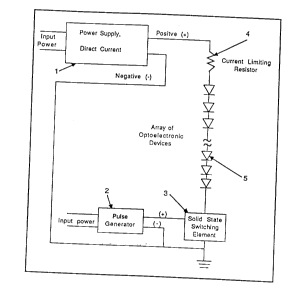
FIG. 1 is a block diagram, illustrating the
components of the apparatus used to provide the light
required by plants for growth and developement;
FIG. 2 is an illustration of the asymmetrical
wave f orm;
FIG. 3 is a block diagram, illustrating the
pulse generator that generates the asymmetric pulses to
the electric power driving components;
FIG. 4 is a circuit diagram, illustrating the
solid state switching element and components that drive
the optoelectronic device array;
FIG. 5 is a circuit diagram, illustrating the
optoelectronic device array that provides the required
irradiance for plant growth and development; and
FIG. 6 is a fragmentary perspective view,
illustrating the optoelectronic device array, the pulse
generator and associated electric power driving
components, and the direct current electric power
supply as a light source for plant lighting.
Detailed Description of the Invention
In FIG. 1, a power supply 1 converts normally
available alternating current (A.C. ) electrical power
to direct current (D.C. ) electrical power which is used
to drive optoelectronic devices. A pulse generator 2
provides a bias current to a solid state switching
element 3 at a preselected fre~uency and duty cycle.
Current flows through a current limiting resistor 4 and
an optoelectronic device array 5 only during the time a
bias current is applied to the solid state switching
element 3. The current flowing through each
optoelectronic device in array 5 results in emission of
radiant energy from the device. The spectral
characteristics of the emitted radiant energy depends
on the composition of the materials used in the
fabrication of the optoelectronic device. The current
--6--
_7_ 2~17~ 3
limiting resistor 4 limits the amount of current to the
optoelectronic devices to prevent excessive current
from passing through the device and causing a failure.
FIG. 2 illustrates an asymmetrical wave form
that is used to pulse the optoelectronic device array
5. Time period Tl designated by the numeral 6 is the
duration time the electric power is applied to the
optoelectronic device array 5. Time period T2
designated by the numeral 7 is the duration time no
electric power is applied to the optoelectronic device
array 5. Time period T3 designated by the numeral 8 is
the duration of one pulse cycle. The electrical
potential of the Tl 6 pulse must be adequate to cause
the solid state driving components to conduct electric
current from the optoelectronic device array 5 to
ground. The electric potential of the T2 7 pulse must
be low enough to not allow any current to pass from the
optoelectronic device array 5 through the solid state
driving components to ground.
FIG. 3 is a block diagram of the components
of pulse generator 2 that provide the asymmetrical wave
form. A time base ~enerator 9 is an integrat~d circuit
capable of producing pulses with a time duration from
100 nanoseconds to 10 microseconds. Both cycle counter
10 and duration coun~:er 11 are integrated circuits
capable of counting pulses generated by the time base
generator 9. The cycle counte 10 output provides a
timing pulse for every time period T3 8. This timing
pulse triggers the duration counter 11, thereby
enabling duration counter 11 output to switch to the Tl
6 state. The output of ~:he duration counter 11 remains
in the Tl 6 state until a specified count has been
reached. When the specif ied number of pulses are
counted by the duration counter 11 the output switches
to ~he T2 7 state. The T2 7 output state activates the
--7--
-8- 2a4
reset input to the duration counter 11 and thus
preventing additional counting of the pulses generated
by the time base generator 9. The next pulse from
cycle counter 10 inactivates the reset input of the
5 duration counter 11 which initiates a repeat of the
t imi ng cycle .
Pulsing the electrical power to the
optoelectronic device array accomplishes two
purposes: (1) an asymmetric pulse allows driving the
10 optoelectronic device array at power levels far in
excess of continuous duty levels, thereby providing the
irradiation levels required for plant growth and
development, and (2) the asymmetrical pulsing cycle can
be synchronized to the time constants of the various
15 aspects of the energy gathering and energy conversion
processes of photosynthesis. This results in a high
efficiency of converting electricity to irradiation for
plant growth and development.
An alternative to the functions provided by
20 the components shown in FIG. 3 could be provided by
using a microprocessor programmed to accomplish the
described functions, or operate ~he optoelectronic
devices in a continuous mode.
FIG. 4 is a circuit diagram of the solid
25 stat~ switching element 3. The components of the solid
state switching element 3 include a base resistor 12
and a power switching device 13, such as a power
transistor. The function of the power switching device
13 is to control the current passing from the
30 optoelectronic device array 5 to ground. During the T
6 time period the power switching device 13 allows
current to pass irom the optoelectronic device array 5
to ground. During the time period T2 7, the power
switching device is in a high impedance state thereby
35 preventing flow of current from the optoele~tronic
--8--
9 2~17~3
device array 5 to ground. 3ase resistor 12 is sized to
assure that sufficient base current is provided to
saturate the power switching device 13 during the Tl 6
time period.
The optoelectronic device array 5 shown in
FIG. 5 consists of a number of devices connected both
in series and in parallel. The optoelectronic device
14 is a light emitting diode having a peak emission
between 620 and 680 nm. This light emitting diode
represents the majority of devices in the array because
it provides the radiant energy that interacts with the
chlorophyll molecule to produce the "excited" state.
The peak emission of light emitting diode 14 coincides
with one of the absorption peaks of chlorophyll . This
matching of light emitting diode 14 to the absorption
peak of chlorophyll is one of the contributin~ factors
toward the electrical efficiency of this invention in
providing light for plant growth.
A number of light emitting diodes 14 are
connected in series to the direct current power supply
1 with a current limiting resistor 15. The number of
light emitting diodes 14 connected in series and the
value of the current limiting resistor 15 are dependent
on the voltage of the direct current power supply 1,
the electrical characteristics of light emitting diode
14, and the desired level of current applied to light
emitting diode 14. A sufficient number of these
series-connected light emitting diodes 14 are connected
in parallel to the direct current power supply 1.
These parallel arrays would be arranged in a panel
conf iguration and the panels would be mounted in a
ganged fashion to irradiate a large plant growir.g area.
Optoelectronic device 16 is a light emitting
diode with a peak emission range of 700-760 nm. This
radiant energy is required ior excitation of the
_g_
20417t 3
--10--
photobiologically active molecules involved in a number
of photomorphogenic responses of plants. Radiant
energy at 700 to 760 nm is also involved in enhancing
the energy transformation processes involved in
photosynthesis. The number of light emitting diodes 16
in the total optoelectronic array is much less than the
number of light emitting diodes 14 because only a small
amount of radiant energy is required to produce the
desired photomorphogenic responses. As was previously
described, the light emitting diodes 16 are connected
in series to the direct current power supply 1 with a
current limiting resistor 17. The number of light
emitting diodes 16 connected in series and the value of
current limiting resistor 17 are dependent on the
voltage of the direct current power supply 1, the
electrical characterisitcs of light emitting diode 16,
and the desired current to be applied to light emitting
diode 16. A sufficient number of these series-
connected light emitting diodes 16 are connected in
parallel to the direct current power supply 1 to
provide the desired level of irradiance in the spectral
region of 700-760 nm.
Optoelectronic device 18 is either a light
emitting diode or a neon lamp, either of which emit
radiant energy in the spectral region of 400 to 500
nm. This radiant energy is required for excitation of
the photobiologically active molecules involved in the
synthesis of chlorophyll and the phototropic and other
photomorphogenic responses of plants. The number of
optoelectronic devices 18 in the total optoelectronic
array is approximately the same as the rlumber of light
emitting diodes 16 and much less than the number of
light emitting diodes 14 because only a small amount of
radiant energy is required to produce the desired
photomorphogenic and phototropic responses. The
--10--
--ll--
2~17~3
optoelectronic devices 18 are connected in series to
the direct current power supply 1 with a current
limiting resistor 19. The number of optoelectronic
devices 18 and the value of current limiting resistor
5 19 are dependent on the voltage of the direct current
power supply 1, the electrical characteristics of the
optoelectronic device 18, and the desired current to be
applied to optoelectronic device 18. These conditions
are particularly important if a light emitting diode or
10 a neon lamp is selected as the device of choice. A
sufficient number of these series-connected
optoelectronic devices 18 are connected in parallel to
the direct current power supply 1 to provide the
desired level of irradiance in the spectral region of
40~ to 500 nm.
FIG. 6 illustrates a fragmentary perspective
view of an exemplary lighting unit described in this
disclosure. The optoelectronic array 5 is mounted on a
board 20 with a reflecting lower surface. The
20 reflecting lower surface directs a maximum amount of
the radiant energy emitted by the devices toward the
plant growing surface located parallel to the
optoelectronic device array 5. The current limiting
resistors 4 are also mounted on board 20. The direct
25 current power supply 1, the pulse generator 2, and the
solid state switching element 3 are mounted on board 21
positioned above the optoelectronic device array board
20. This arrangement of boards 20 and 21 would allow
for cooling the electronic components if desired.
30 Boards 20 and 21 function effectively in any mounting
position so as to facilitate the use of this lighting
system in various types of applications.
--11--
--12--
2~1713
Various modes of carrying out the invention
are contemplated as being within the scope of the
following claims particularly pointing out and
distinctly claiming the subject matter regarded as the
invention .