Note: Descriptions are shown in the official language in which they were submitted.
2 ~ 9
l BACKGROUND OF THE INVENTION
Field of the Invention
The present invention relat.es to a waveform
displaying device, which can be utilized for a digital
oscilloscope, etc. reproducing to display waveform of
a measured analogue signal on the basis of waveform
data, into which the measured analogue signal is digital-
converted.
Description of the Related Art
~ waveform observing device such as a digital
oscilloscope, etc. is provided with an analogue to
digital converter, a waveform memory and a waveform
displaying device. It stores waveform data obtained by
converting an observed analogue signal into a digital
signal with a predetermined period by means of the
analogue to digital converter in the waveform memory
and reads out the waveform data stated above at need
from the waveform memory to transfer them to the waveform
displaying device in order to reproduce to display the
waveform of the measured analogue signal described
above. Heretofore the waveform displaying device
converts digital waveform data into an analogue signal
by means of a digital to analogue converter and effects
the reproduction and the display of the waveform by
using this analogue signal as a deflection signal for
~41~4~
1 a CRT. However, if a number of different waveforms are
displayed by such a waveform displaying device, the
scanning distance with a beam in the CRT becomes long
and the display brightness is reduced. Eurther, since
it is necessary to sweep the beam with a high speed in
order to prevent fluctuations in the display, the CRT
is restricted to be of electrostatic deflection type.
The depth of an electrostatic deflection type CRT is
great with respect to the display area and it cannot be
desired to reduce the size of the device.
On the other hand, recently a waveform
displaying device provided with a pixel memory and a
display device, in which the display is effected by
controlling brightness of pixels; e.g. a raster scanning
display or a liquid crystal display, is used in practice.
The waveform displaying device stated above is so
constructed that interpolation processing is executed
between different waveform data by a CPU; the waveform
is traced in the pixel memory; and the waveform is
reproduced to be displayed by transmitting successively
brightness information stored in this pixel memory to
the display device.
When the waveform displayinq device described
above is used, in the case where a number of different
waveforms are displayed, since these waveforms are
synthesized in the pixel memory, the brightness of the
display is not reduced. Further, the depth of the
raster scanning display or the liquid crystal display
.
,
~4~
1 is smaller than that of the electrostatic deflection type
CRT, Which makes it possible to reduce the size of the
device.
However, since the display resolving power
of the raster scanning display or the liquid crystal
display is not so high, in the case where the number of
waveform data is greater than the number of display
pixels, a method, by which the maximum value and the
minimum value are detected for every predetermined
period of time and only interpolation lines connecting
these data are displayed are used. By such a method,
since many waveform data have been already thinned out,
much information is lost. When it is displayed, a
uniform band is formed and therefore it is impossible
to find variations in the slew rate and the phase.
SUMMARY OF T~E INVENTION
~ The present invention has been done in order
to solve the problems of the conventional technique
described above and the object thereof is to provide
an excellent waveform displaying device capable of
displaying waveform data of large quantity, without
losing any information which they have.
In order to achieve the above object, a wave-
form displaying device according to the present invention,
which reproduces to display a waveform of a measured
analogue signaI on the-basis of waveform data, into
which the measured analogue signal is digital-converted
2~41949
1 by means of an analogue to digital converter, is
characterized in that it comprises displaying means for
effecting the display while controlling the brightness
of pixels; a pixel memory for outputting the brightness
of pixels to the displaying means stated above; inter-
polation line brightness generating means for obtaining
the brightness of each of interpolation lines by using
differences between inputted waveform data; and bright-
ness accumulating means for accumulating the brightness
of the interpolation lines from the interpolation line
brightness generating means stated above in the corre-
sponding pixels in the pixel memory.
- In this way, according to the present invention,
the brightness is varied, depending on the slew rate
of waveform, if the brightness of the relevant inter-
polation line is increased, e.g. when differences
between waveform data are small, and on the contrary
the brightness of the relevant interpolation line is
decreased, when the differences are great. Further,
places where the density of waveform is high are displayed
brightly by the accumulation of the brightness. That
is, since variations in the waveform are displayed
together with information on the brightness, it is
possible to display waveform data of large quantity even
by using a display device having a low resolving power.
BRIEF DESCRIPTION OF THE DRAWING
Fig. 1 is a schematical block diagram sho~ing
; _ 4 _
.
., .
~' ' ' , '
.,
. .
1 a waveform displayiny device in an embodiment of ~he
present invention.
DESCRIPTION OF THE PREFERR~D EMsoDIMENTs
~ ereinbelow the ~resent invention will be
explained, referring to the drawing.
Fig. 1 is a block diagram indicating an
embodiment of the waveform displaying device according
to the present invention.
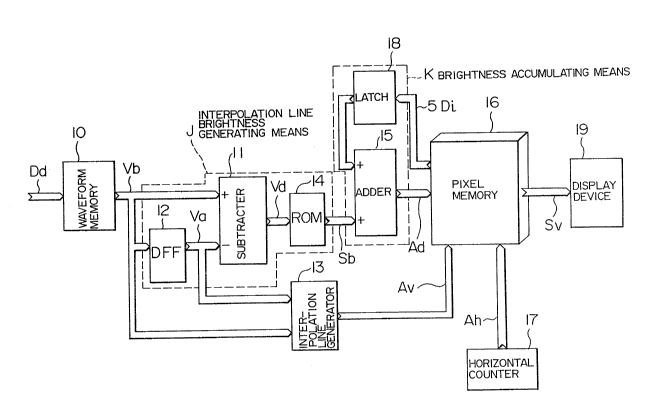
In Fig. 1, a waveform memory 10 takes waveform
data Dd from an analogue to digital converter to store
them. The waveform data stored in the waveform memory
10 are inputted in a subtracter 11, a D flipflop
(hereinbelow called "DFF") 12 and an interpolation line
genexator 13. The DFF 12 outputs waveform data Va
preceding directly waveform data Vb. These waveform
data Va are inputted in the subtracter 11 and the inter-
polation line generator 13. In this way the subtracter
11 calculates the difference Vd between the waveform
data Va and the waveform data Vb inputted therein to
output it. This difference output Vd of the subtracter
11 is inputted in an address of a brightness calculating
ROM 14. The ROM 14 outputs brightness data Sb of an
interpolation line, responding to the difference Vd.
The brightness data Sb described above is inputted in
an adder 15. Here the substracter 11, the DFF 12 and
the ROM 14 constitute interpolation line brightness
generating means J.
.
.. . -...................... .
1 The interpolation line 13 generates successive-
ly vertical addresses for all the pixels corresponding
to the interpolation line of the inputted waveform data
from Va to Vb. The addresses generated by the inter-
polation line generator 13 are inputted in verticaladdress Av of the pixel memory 16. A horizontal counter
17 specifies the horizontal position of the interpolation
line and the output of this horizontal counter 17 is
inputted in horizontal address Ah of the pixel memory
16. The pixel memory 16 outputs brightness data Di of
the pixels specified by the vertical address Av and
the horizontal address Ah. These brightness data Di are
inputted in a latch 18 and held therein. The output of
the latch 18 is inputted in an adder 15 to be added
there to brightness data Sb of the interpolation line.
This adder 15 and the latch 18 constitute brightness
accumulating means K.
The output of the adder 15 is written in the
pixel memory 16 as the brightness data for the pixels
specified by the vertical address Av and the horizontal
address Ah described above. The display device 19 reads
out successively the brightness data Sv from the pixel
memory 16 to display them.
The waveform displaying device constructed
as described above will be explained, referring to Fig.
1.
The waveform data converted into a digital
signal by means of an analogue to digital con~erter,
:. .
.
1 with a predetermined period are stored in the waveform
memory 10. When waveform data for one frame are written
in the waveform memory 10, it outputs successively the
- waveform data Vb for the display. The waveform data Vb
are inputted in the subtracter 11, the ~FF 12 and the
interpolation line generator 13. The DFF 12 outputs
the waveform data Va prece~ing directly the waveform
data Vb outputted by the waveform memory 10. In ~his
way, the subtracter 11 calculates the difference
Vd = Vb - Va between the two waveform data sets.
The brightness of the interpolation line is
calculated by inputting the difference Vd of the wave-
form data in the ROM 14. The brightness I calculated
by using e.g. a following formula;
I = k/¦Vd¦ + 1 ... (1)
is written in the ROM 14 in the form of a table.
In this Eq. (1) ¦Vd¦ represents the absolute
value of the difference of the waveform data and k is
a constant.
By the method as described in the above example
the part, where the slew rate of the waveform is high,
is displayed darkly and the part, where the slew rate
is low, is displayed brightly. The brightness data Sb
are inputted in the adder 15.
In the case where the waveform is reproduced
~5 to be traced in the pixel memory 16, it is necessary
to interpolate the waveform data by using a line.
: . .
.
4 ~
1 In the case where the number of waveform data sets in
one frame is greater than the number of display pixels
in the horizontal direction, the interpolation line is
a straight line in the vertical direction. Consequently,
in order ~o trace an interpolation line from the wave-
form data Vb to Va, the brightness of the interpolation
line may be written in all the pixels in the vertical
direction from Vb to Va.
` In order to realize it, the interpolation line
generator 13 generates successively vertical address
Av from the inputted waveform data Vb to Va. The
vertical address Av described above and the horizontal
address Ah generated by the horizontal counter 17 are
inputted in the pixel memory 16. In this way all the
pixels of the interpolation line are accessed one after
another and the brightness of each of the pixels is
increased by the respective brightness of the interpola-
tion line by the latch 18 and the adder 15. In the case
where the number of waveform data sets in one frame is
n times as great as the number of display pixels in the
horizontal direction, n interpolation lines in~the
vertical direction are written in a same horizontal
address, superposed on each other. In order that no
brightness information is lost by the superposed writing,
the brightness is accumulated by the latch 18 and the
adder 15. When one interpolation line has been once
traced, the output of the DFF 12 is updated and the
waveform memory 10 outputs following waveform data.
.
.
~19~9
l Thereafter succeeding interpolation lines are
traced in the same manner as described above. In the
case where the number of waveform data sets in ~n~ ~rame
is n times as great as the number of display pixels in
the horizontal direction, as described previously,
every time n interpolation lines are traced, the
horizontal address Ah in the horizontal counter 17 is
increased by 1. When the trace of one frame is
- terminated, the brightness information is transferred
to the display device l9 to be displayed there.
In the case where a number of waveforms are
displayed, if the waveforms are accumulated in the pixel
memory on each other, parts where waveforms are super-
posed are displayed brightly.
As clearly seen from the embodiment described
above, according to the present invention, since the
brightness of the interpolation line is varied, depending
on the slew rate and the brightness is accumulated by
superposing interpolation lines, even in the case where
a dense waveform having a high frequency is displayed,
points, at which the phase, the frequency or the amplitude
is varied, are displayed as points, at which the bright-
ness is varied, and therefore an effect can be obtained
that it is possible to find easily peculiar points in
the waveform. further, according to the present
invention, it is possible to display a number of wave-
forms and another effect can be obtained that observation
is easier, because superposed parts become clearer.
' ~'
. .