Note: Descriptions are shown in the official language in which they were submitted.
20421 02
G-2,500 C-4,262
MDI FAULT DETECTION CIRCUIT
WITH DVAL MODE FAULT DETECTION
Background of the Invention
This invention relates to fault detection
apparatus for a motor driver interface circuit. Such
an interface circuit is disclosed which connects motor
power drive apparatus to a computer control and allows
motor operation in a plurality of selectable modes,
including bang-bang and PWM operation for reversible
motors connected in an H-bridge configuration and
solenoid mode for a single solenoid device. In each of
these modes the interface circuit may be enabled for
motor or solenoid activation or not so enabled. It is
desired to include fault detection circuitry which
monitors the motor or solenoid for shorts to supply or
ground voltage while the interface circuit is enabled
or not enabled, for shorted load when the interface
circuit is enabled and for open load when the interface
circuit is not enabled. However, the motor voltage and
current conditions for normal and shorted conditions
may be different under enabled and not enabled
conditions.
Summary of the Invention
the apparatus of the invention provides the
desired fault detection by means of circuitry in the
interface circuit which is capable of operation
alternatively in enabled and not enabled modes in
response to the same enable input signal which selects
these modes.
2 20421 02
In particular, the inventive apparatus
comprises an H-bridge electric motor drive apparatus in
which the motor terminals are connected through
resistors sufficiently large to prevent motor
activation therethrough and a not enabled reference
voltage generating apparatus comprising a voltage
divider connected across the first reference voltage to
generate a second reference voltage greater than the
voltage at the first motor terminal with the switching
transistors in an off condition and a third reference
voltage lower than the voltage at the second motor
terminal with the switching transistors in an off
condition, whereby the second and third reference
voltages define a not enabled voltage window
therebetween.
The inventive apparatus further comprises
enabled reference voltage generating apparatus
effective to generate a fourth reference voltage above
the ground voltage terminal at least by the conducting
voltage of one of the switching transistors and a fifth
reference voltage below the supply voltage terminal by
the conducting voltage of the one of the switching
transistors, whereby the fourth reference voltage and
~upply voltage define a first enabled voltage window
therebetween and the fifth reference voltage and ground
define a second enabled voltage window therebetween;
The inventive apparatus further comprises
fault detection apparatus responsive to the enable
signal in its first condition to compare the voltages
at the first and second motor terminals with each of
the second and third reference voltages and signal a
fault if the voltage at one of the first and second
20421 02
motor terminals is outside the not enabled voltage
window and further responsive to the enable signal in
its second condition to compare the voltage at one of
the first and second motor terminals with one of the
fourth and fifth reference voltages and signal a fault
if the voltage at the one of the first and second motor
terminals is outside the corresponding one of the first
and second enabled voltage windows.
Further details and advantages of the
invention will be apparent from the accompanying
drawings and following description of a preferred
embodiment.
Summary of the Drawings
Figure 1 is a block diagram of a motor driver
interface with fault detection apparatus according to
the inventi~,n.
Figure 2 is a circuit and logic diagram of a
gate control for use in the motor driver interface of
Figure 1.
Figure 3 is a circuit and logic diagram of
reference voltage generators, comparators and fault
logic for use in the motor driver interface of Figure
1.
Figure 4 is a circuit diagram showing the
connections of the motor driver interface of Figure 1
to a reversible DC motor in a FET H-bridge arrangement.
Figure 5 is a circuit diagram showing the
connections of the motor driver interface of Figure 1
to a solenoid activating coil.
Description of a Preferred Embodiment
Overall Description of Motor Driver Interface
2042t 02
Referring to Figure 1, a Motor Driver
Interface (MDI) comprises a gate control 10 with four
driver outputs - UGF, UGR, LGF, LGR - each adapted to
provide a gate on/off signal voltage to the gate of a
power FET. These four signals comprise the control
output of the motor driver interface. Gate control 10
receives an external signal PWM, which may take one of
three forms: (1) a rectangular PWM (pulse width
modulated) voltage wave 0/5 volts at a variable duty
cycle, (2) a constant Vcc (5 volts DC), or (3) Vign, a
vehicle ignition voltage of 9-16 volts DC. This signal
indicates the desired mode of operation (PWM,
bang/bang, or solenoid, respectively) and, in the case
of PWM mode, also provides the duty cycle.
Gate Control 1~ is shown in more detail in
Figure 2. The PWM input signal is provided through a
reverse diode 30 to the base of an NPN transistor 31
having a collector tied to chip supply voltage Vcc (5
volts) and an emitter connected through a load resistor
32 to ground, the base of transistor 31 being connected
through a bias resistor 33 to Vcc. The emitter of
transistor 31 is connected to one input of an AND gate
34, the other input of which receives a signal COMPOUT,
to be described. The output of AND gate 34 is provided
to one input of an OR gate 37 and to the input of a MIN
ON timer 38, the output of which is provided to the
other input of OR gate 37. MIN ON timer 38 is
initiated by a positive transition in the output of AND
gate 34 to provide a high output of a predetermined
minimum duration such as 16 microseconds. This ensures
that, when the GATE output of OR gate 37 goes high to
20~21~2
turn on a FET, it stays on for at least the minimum
time, even if the output of AND gate 34 goes low again
before 16 microseconds has elapsed. The reason for
this will be described at a later point in this
description.
The output (GATE) of OR gate 37 is provided to
one input each of AND gates 35 and 36. AND gate 35
receives on its other input a processed forward signal
GF; while AND gate 36 receives on its other input a
processed reverse signal GR. The outputs of AND gates
35 and 36 are provided to inputs of AND gates 27 and
28, respectively; whereas signals GF and GR are
provided to inputs of AND gates 26 and 29,
respectively. Signal EN is inverted in inverter 39,
the output of which is provided to the other inputs of
AND gates 26-29. The outputs of A~'~ gates 26-29,
suitably amplified, are the signals UGF, LGF, LGR and
UGR, respectively.
Referring again to Figure 1, a drive logic
block 11 receives signals F and R, for choosing forward
or reverse motor operation, and a chip select signal
CS, for choosing this particular MDI circuit in a
multi-motor system. Drive logic block 11 generates the
processed forward and reverse signals GF and GR from
signals F and R, respectively, and provides signals GF
and GR to gate control 10, the processing ensuring that
no action is taken if both F and R are high or if they
have not both been constant for a predetermined time.
Drive logic block 11 corresponds to drive logic block
32 and delay block 34 in a U.S. Patent No. 4,924 158,
issued May 8, 1990 and entitled Motor Driver Protection
Circuit.
)421 0~
Signal COMPOUT is provided by a comparator 12,
which compares a current feedback signal with a
predetermined current reference. The current feedback
signal is obtained from inputs ISENHI and ISENLO, which
are connected to the ends of a current sensing resistor
in series with the motor or solenoid to be controlled.
The difference between these input signal voltages is
amplified in a difference amplifier 13 and provide to a
load current simulator circuit 14, the output of which
is provided to one input of comparator 12. Simulator
circuit 14 provides a signal which not only reflects
the load current flowing through the load sensing
resistor but also simulates the recirculation current
through a recirculation current path provided for the
motor or solenoid. The other input of comparator 12
receives the current reference from a digital/-nalog
converter (DAC) 15, which may receive it serially from
a microcomputer 18 by means of a data input circuit 16
and latch 17. Apparatus suitable for use as elements
12-18 to provide a COMPOUT signal for this apparatus is
shown in co-pending U.S. Patent Application 07/340,813,
entitled Method and Apparatus for Inductive Load
Control with Current Simulation, filed April 17, 1989
by the same applicants, and assigned to the assignee of
this application. In particular, that patent
application provides a more detailed description of
simulator circuit 14.
MOTHI and MOTLO signals are obtained from the
armature terminals of the controlled motor or solenoid
and applied to a multiple comparator circuit 20, along
with a series of reference voltages derived from the
vehicle ignition voltage Vign and the chip power supply
-- ~0~21~2
voltage Vcc in reference voltage generator circuit 21.
The outputs of multiple comparator circuit 20 are
provided to a fault logic circuit 22, the outputs of
which are a FAULT signal and a fault code, the code
being latchable by the FAULT signal into a fault
register 23 for serial output to computer 18.
Microcomputer 18 provides control for the
motor or solenoid through the MDI. Microcomputer 18
is the source of signals EN (enable), CS (chip select),
F (forward operation), R (reverse operation), SCLK
(system clock, 2 microseconds), and PWM. In addition,
microcomputer 18 provides a serial clock (SERCLK) and
data in (DI) and data out (DO) channels and receives
the FAULT signal.
Motor or Solenoid Connections
The connection arrangement for a rotating DC
motor is shown in Figure 4. A reversible DC permanent
magnet motor 110 has a rotating armature with a
standard commutator and brushes 111, 112 defining motor
armature terminals, the voltages at which are sensed as
signals MOTHI and MOTLO, respectively. Brush 111 is
connected through a resistor 120 to Vcc; and brush 112
is connected through a resistor 121 to ground.
Resistors 120 and 121 have resistance values much
greater than the impedance of the motor armature so
that neither will carry current sufficient, at the
supply voltage indicated, to activate motor 110 (for
example, 1.6K and 2.4K, respectively). The arrangement
is used only for voltage sensing in the not enabled
state, as will be described with reference to the FAULT
-- 2042102
determination circuit of Figure 3. The operation of
motor 110 is controlled through a power FET H-bridge
circuit. Brush 111 is connected through a power FET
113 to Vign and through a power FET 114 and resistor
115 in series to ground. Likewise, brush 112 is
connected through a power FET 116 to Vign and through a
power FET 117 and resistor 115 to ground. Resistor 115
is a low resistance, high power (0.01 ohm, 2W), current
sensing resistor. The junction of the sources of power
FETs 114 and 117 and the ungrounded end of resistor 115
provides a voltage signal ISENHI, while the grounded
end of resistor 115 provides a voltage signal ISENLO.
The output signals of the motor driver interface are
provided to the gates of the FETs: UGF to FET 113, LGR
to FET 114, UGR to FET 116 and LGF to FET 117. Each of
FETs 113, 114, 116 and 117 is provided with a parallel,
reverse oriented diode (122, 123, 124, 125,
respectively) for recirculation current in the normal
manner for such arrangements.
A solenoid driving arrangement is shown in
Figure 5. Solenoid 130 comprises a coil 130 with one
end connected to Vign and the other connected through a
power FET 131 and a current sensing resistor 132 to
ground. The junction of solenoid 130 and the drain of
FET 131 is connected through a resistor 133 to ground
and provides a voltage signal MOTLO; while voltage
signals ISENHI and ISENLO are provided from the
ungrounded and grounded ends, respectively, of current
sensing resistor 132. As with re8istors 120 and 121,
the resistance of resistor 133 is much greater than
that of the controlled load, in this case solenoid 130,
so that it does not provide a series activating current
20421~2
path for the load. The gate of FET 131 is provided
with signal LGF from gate control 10 in this
embodiment, although signal LGR could have been chosen.
A current recirculating diode 134 is provided in
parallel with solenoid coil 130.
Basic Operation and Mode Selection
Referring to Figure 2, the voltage at the
emitter of transistor 31, which is one input to AND
gate 34, follows the PWM input. AND gate 34 thus
combines signals PWM and COMPOUT and provides its
output, along with that of MIN ON timer 38, through OR
gate 37 as a GATE signal to AND gates 35 and 36, only
one of which may be enabled at a time, due to signals
GF and GR. Thus, motor control is achieved in response
to an enable signal EN, a forward/reverse direction
signal (F or R), a mode select signal PWM, a current
reference signal from a computer, and a current
feedback signal (ISENHI-ISENLO) from the motor.
Assuming the MDI is connected as shown in
Figure 4 to control a motor 110, the chip is enabled
(EN low) and forward motor operation is selected, upper
power FET 113 is continuously activated by signal UGF
and lower power FET 117 is turned on and off by signal
LGF in response to the GATE signal output of OR gate 37
through AND gate 35, which is enabled by signal GF, and
AND gate 27, which is enabled by EN low. Upper power
FET 113, in addition to providing part of the motor
current path when lower power FET 117 is turned on,
also provides with diode 124 a recirculating current
path for the inductive motor armature coil when lower
20~2102
power FET 117 is turned off. FETS 116 and 114 are
turned off at this time by the low GR signal providing
low LGR and UGR signals.
A bang/bang mode of operation may be selected
by providing a constant Vcc (5 volts) at the PWM input.
Thus, the input to AND gate 34 from transistor 31 is
continuously high; and the output of AND gate 34 is
controlled in response to COMPOUT, the output of
comparator 12, as modified by MIN ON timer 38.
Comparator 12 compares a simulated motor current level,
derived from the motor current sensing resistor 115 by
means of voltage signals ISENLO and ISENHI, difference
amplifier 13 and load current simulator 14, with a
predetermined reference provided from computer 18
through data apparatus 16, latch 17 and DAC 15. The
operation of suitable apparatus is described in more
detail in the aforementioned patent application
07/340,813. Briefly, however, when FET 117 is turned
on, the apparatus compares a voltage simulating the
increasing motor load current with a predetermined
reference and provides a high COMPOUT signal to AND
gate 34 to continue conduction of FET 117 until the
simulated motor load current exceeds the reference by
an amount sufficient to switch the comparator output
COMPOUT low (and the minimum ON time is exceeded).
While the motor load current increases, a capacitor in
simulator 14 is also charged at a rate simulating the
build-up of magnetic energy in the motor armature
windings. When COMPOUT goes low, FET 117 iS disabled.
The capacitor in simulator 14 is discharged to simulate
the decreasing recirculation current, which is not
measured by current sensing resistor 115 and must thus
- ~0~2~02
be simulated. When this simulated current falls below
the reference by an amount sufficient to switch the
comparator output COMPOUT high, FET 117 is again
enabled and the cycle repeated. In bang/bang mode, the
motor load current will thus be controlled to an
average value determined by the operator controllable
predetermined current reference supplied from computer
18.
If reverse motor operation is selected, the GR
signal activates upper power FET 116 continuously,
while lower power FET 114 is controlled by AND gate 34
through AND gate 36 and FETs 113 and 117 are turned off
by the low GE signal. Apparatus such as that described
in aforementioned patent application 4,924,158 is
provided to ensure that forward and reverse signals
cannot be provided simultaneously; and such apparatus
protects the power FETs connected to the same motor
brush from being simultaneously turned on with a
resulting direct short circuit of the power supply.
In either the forward or the reverse
direction, the MDI can also be operated in a PWM mode.
For PWM mode, the predetermined reference supplied
through DAC 15 is set to a high value so that COMPOUT
~tays continuously high; and a rectangular PWM signal
alternating between Vcc (5 volts) and ground is
provided at the PWM input. In this mode, control of
AND gate 34 is given to the PWM signal, which
determines the average motor load current through its
duty cycle. The PWM mode can be modified, if desired,
by providing a predetermined current reference through
DAC 15 which is high but not the highest possible value
so as to normally provide PWM operation but still limit
20~2102
abnormally high motor load currents by shortening only
those "on" pulses of the PWM signal which are
sufficiently long to allow the simulated motor load
current to exceed the reference. Of course, the
MIN ON timer is also activated by the PWM signal.
A solenoid control mode is similar to the
bang/bang mode except that Vign (9-16 volts) is
provided to the PWM input. A single FET 131, as seen
in Figure 5, is connected to receive output signal LGF
(alternatively, signal LGR could be chosen), so that
forward operation is selected with signal F. The upper
FET is not needed, since solenoid coil 130 need be
activated in only one direction and its recirculating
current diode 134 may be placed in parallel with the
coil. The switching of FET 131 is similar to that
exercised n the bang/bang mode, with average solenoid
current being self regulating about a predetermined
reference provided through DAC 15. The major
difference between this mode and bang/bang mode is in
the external solenoid connections and in the fault
detection, which is yet to be described.
Fault Detection
Now that the structure and operation of the
MDI has been described, the fault detection apparatus
can be understood. The fault detection circuit is
shown in detail in Figure 3. The circuit provides
detection of open or shorted loads, shorts to ground
and shorts to Vign during static (not enabled, EN high)
or dynamic (enabled, EN low) operation. The basic
inputs to the fault detection circuit are the MOTHI and
2~12~0~
MOTLO signals from the two motor brushes, the enable
signal EN (which distinguishes enabled and not enabled
modes), and the PWM signal (which distinguishes
solenoid and motor control modes). The circuit also
uses, in the enabled state, the F, R and GATE signals.
When the MDI circuit or chip is not enabled
(EN high), the motor armature provides a low impedance
path (about 0.50 ohms) through the armature windings
between the brushes; and the FETs are off to present
high impedance paths to Vign and ground. Thus, with
reference to Figure 4, MOTHI and MOTLO should both be
at essentially the same voltage determined by the
voltage-divider of resistors 120 (1.6K) and 121 (2.4K)
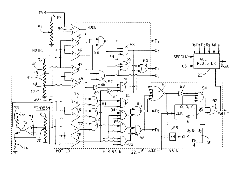
across Vcc. Referring to Figure 3, resistors 40, 41
and 42 (50K each), connected in series across the same
voltage Vcc, define a voltage window between junction
43 of resistors 40 and 41 and junction 44 of resistors
41 and 42. Both MOTHI and MOTLO should be within this
voltage window (that is, between the voltages at
junctions 43 and 44) when all FETs are off. Junction
43 is thus connected to the non-inverting inputs of
comparators 45 and 47; and junction 44 is connected to
the inverting inputs of comparators 46 and 48. MOTHI
is provided to the inverting input of comparator 45 and
the non-inverting input of comparator 46; while MOTLO
is provided to the inverting input of comparator 47 and
the non-inverting input of comparator 48.
The PWM input is provided to the inverting
input of a comparator 50 having a non-inverting input
provided with a reference voltage from a voltage
divider 51 across Vign. This voltage divider 51
provides a voltage just less than Vign, so that the
20ll21~2
14
MODE signal output of comparator 50 is high in the PWM
and bang/bang modes of operation, when the PWM voltage
is never higher than Vcc (5 volts). On the other hand,
in the solenoid drive mode of operation, when Vign
(9-16 volts) is provided to the PWM input, the MODE
signal is forced low.
The outputs of comparators 45 and 47 are
connected to the inputs of a NAND gate 56 providing an
output D4; while the outputs of comparators 46 and 48
are connected to the inputs of a NAND gate 57, which
provides an output D5. The outputs of NAND gates 56 and
57 are connected to inputs of AND gates 58 and 59,
respectively; and each of AND gates 58 and 59 has an
input provided with the enable signal EN and another
input provided with the MODE signal from the output of
comparator 50. The output of AND ~ate 58 provides a
signal Do; while the output of AND gate 59 is connected
to one input of an OR gate 60 having another input,
with connection to be described, and an output
providing a signal D1.
In operation, comparators 45-48 will provide
outputs indicating whether MOTHI and MOTLO are within
the defined voltage window. If they are (no faults),
each of comparators 45-48 will have a high output; and
D5, D4, Dl and Do will all be low (0). A short of
either side of motor 110 to Vign or ground or an open
load will cause one or more of the comparators 45-48 to
change its output state to a low output. A comparator
output indicating a fault will be passed by AND gates
58 and 59 only when one of the motor control modes (PWM
or bang/bang, not solenoid mode) is selected (MODE
high) and the MDI circuit is not enabled (EN high).
14
2042192
The detected fault will be indicated in the output
signals Dl,Do forming a static (not enabled) fault
status code which comprises the least significant bits
of a fault status byte and are both low when no errors
are present, due to the high outputs of comparators
45-48. If MOTHI shorts to Vign, comparator 45 will
switch low. If MOTLO shorts to Vign, comparator 47 will
switch low. Either of these changes will switch Do
high; and 0,1 is thus the static fault status code in
D1,Do for short to Vign. Likewise, a short of either
MOTHI or MOTLO to ground causes a static fault status
code of 1,0; and an open load causes a static fault
status code of 1,1. Bits D5 and D4 of the fault status
byte, which are not affected by the EN and MODE signals
are of use when the EN signal is low (enabled) but the
chip output has been turned off due to the detection of
a dynamic (enabled) error.
In the enabled state, when the EN signal is
low, at least one of the upper FETs 113 and 116 and and
sometimes one of the lower FETs 114 and 117 will be
turned on; and MOTHI and MOTLO will have quite
different desired voltage ranges from those expected in
the not enabled state. Thus a different error
detection arrangement is required. The EN signal thus
disables AND gates 58 and 59 to guarantee a 0,0 static
error status code in D1,Do. Generally, one side of
motor 110 - MOTHI or MOTLO, depending on whether
forward or reverse motor drive is selected - will be
only a small voltage drop of a conducting FET lower
than Vign, while the other side will be a similar
voltage drop up from ground if the lower FET is
conducting or at a high voltage substantially the same
2042102
as the one side of the motor if the lower FET is not
conducting. Voltage windows are therefore defined with
reference to some voltage FTHRESH above ground and the
same voltage less than Vign, where FTHRESH ( for
example, 3 volts) is greater than the source/drain
voltage of a conducting power FET. In normal
operation, a motor terminal can be expected to be
within one of these windows.
A reference voltage generator comprises a
voltage divider 70 across Vcc generating the reference
voltage FTHRESH, which is provided to the inverting
inputs of comparators 76 and 78. FTHRESH is also
provided to the non-inverting input of an op-amp 71
having an output connected back to its inverting input
and also to the base of an NPN transistor 72 having a
collector connected through a resistor 73 to Vign and
an emitter connected through a resistor 74 to ground.
The collector of transistor 72, which is thus
maintained at a voltage Vign minus FTHRESH, is provided
to the non-inverting inputs of comparators 75 and 77.
MOTHI is provided to the inverting input of comparator
75 and the non-inverting input of comparator 76; while
MOTLO iS provided to the inverting input of comparator
77 and the non-inverting input of comparator 78.
The outputs of comparators 75, 76 and 77 are
provided to inputs of AND gates 80, 81 and 82,
respectively, each of which AND gates is further
provided with the MODE si gnal on its other input. The
output of comparator 78 is not gated by the MODE signal
and is thus the only comparator to be effective in
error determination in solenoid drive mode. Since the
allowed values of MOTHI and MOTLO are different for
- ~D~2102
forward and reverse motor drive, this information must
enter the logic. The output of AND gate 80 is provided
to an input of a NAND gate 83, which has an additional
input of the forward drive signal F. The output of AND
gate 81 is provided to an input of a NAND gate 84,
which has additional inputs of the reverse signal R and
the GATE signal tfrom Figure 2). The output of AND
gate 82 is provided to an input of a NAND gate 85,
which has an additional input of the reverse drive
signal R. The output of comparator 78 is connected to
an input of a NAND gate 86, which has additional inputs
of the forward drive signal F and GATE. A NAND gate 87
has inputs connected to the outputs of NAND gates 84
and 86 and an output providing a signal D2. A NAND
gate 88 has inputs connected to the outputs of NAND
gates 83 and 85 and an output providing a signal D3.
Signals D3 and D2 provide a two bit dynamic fault
status code and form the third and fourth least
significant bits of the fault status byte.
With no faults, comparator 75 will have a low
output for forward operation, since upper FET 113 will
be turned on. This will produce a low output from AND
gate 80 and a high output from NAND gate 83. In
forward operation, the low signal R will guarantee a
high output from NAND gates 84 and 85. If the lower
FET 117 is gated on, the output of comparator 78 will
be low; but if it is gated off, the GATE signal will be
low. In either case, the output of NAND gate 86 will
be high. Thus, the outputs of NAND gates 83-86 will
all be high; and signals D3 and D2 will both be low
(0,0). Similar analysis shows the same no fault output
for reverse operation, with upper FET 116 turned on and
2~42102
18
lower FET 114 gated on or off.
In forward enabled operation, the circuit is
able to detect a short of MOTHI to ground, regardless
of the conducting state of lower FET 117, as comparator
75 switches high to switch NAND gate 83 low and
generate a D3,D2 output of 1,0. Detection of a short
of MOTLO to Vign, however, can only be detected when
FET 117 is turned on. In this case, comparator 78
switches high; and NAND gate 86, receiving additional
high inputs from GATE and EN, switches low to cause a
D3,D2 output of 0,1. Reverse enabled operation is
similar but uses comparator 77 and NAND gate 85 to
detect a short of MOTLO to vign for a D3,D2 output of
0,1 and uses comparator 76 and NAND gate 84 to detect a
short of MOTHI to ground and produce a D3,D2 output of
1,0. If the load is shorted, the outputs of
comparators 75-78 are all high with the appropriate
lower FET turned on. For forward or reverse operation,
this will produce a D3,D2 output of 1,1 with a high
GATE si gnal.
For solenoid drive, only comparator 78 matters
(assuming the solenoid is connected between MOTLO and
ground as in Figure 5); and the outputs of comparators
75-77 are thus gated low in response to a low MODE
signal as previously described. In the enabled state
(EN low), D3 is held at "O" while bit D2 goes to "1"
with a short of MOTLO to Vign. In the not enabled
state (EN high), there will be no high GATE signal; so
the D2 signal remains low. However, additional
circuitry is provided to detect a short to ground in
the not enabled state. The MODE signal from comparator
50 is inverted by an inverter 66 and provided to one
18
20~2102
19
input of an AND gate 90. Signal EN is provided to
another input of AND gate 90. Finally, the third and
last input of AND gate 90 receives the output of
comparator 78 inverted by an inverter 67. AND gate 90
has an output connected to an input of OR gate 60 and
thus provides a high output for D1 when solenoid mode
is selected, the MDI circuit is not enabled, and
comparator 78 detects a short to ground.
The circuit further creates a digital FAULT
signal which goes high when a fault is present and low
when no fault is present. The outputs of AND gates 58
and 59, NAND gates 87 and 88, and AND gate 90 are
provided to the inputs of NOR gate 61, which will thus
go low if a "1" bit appears in any of D3, D2, D1, and
Do~ The output of NOR gate 61 is provided to the reset
MR input of a timer 91; and the SCLK signal (a pulse
every 2 microseconds) is provided through a
divide-by-four circuit to the CLK input of timer 91,
which is thereby clocked every 8 microseconds. The Q2
output of timer 91 is connected to the input of an OR
gate 92, the output of which is the FAULT signal.
Timer 91 is released to start counting clock pulses
when the output of NOR gate 61 goes low; and, if NOR
gate 61 has remained continuously low until the Q2
output of timer 91 goes high (after 24 microseconds),
FAULT is sent high to latch bits D7-Do into fault
register 23 (D7 may be the FAULT signal itself and D6
may be any other fault signal bit). The fault
condition must be continuous for the 24 microseconds,
since its discontinuation will provide a low signal to
the MR input for a stop and reset of timer 91. The
requirement of a continuous fault signal for 24
19
2~21(12
microseconds before latching provides noise filtering
in both the enabled and not enabled states to reduce
the chance of false fault detection. The FETS are
chosen for their ability to withstand short circuit
currents for at least 50 microseconds, which allows
time for this filtering.
However, the output of NOR gate 61 is further
provided through an inverter 93 to one input of an AND
gate 94. AND gate 94 has other inputs from the Q2' Ql
and Q0 outputs of another timer 95, which receives SCLK
clock pulses every 2 microseconds on a CLK input and
signal GATE on an MR reset input. The output of AND
gate 94 is provided to the other input of OR gate 92.
If NOR gate 61 goes low, timer 95 will generate a FAULT
signal on the seventh count (14 microseconds) after a
lower FET is turned on (GATE goes high) if a fault
condition exists at the time, since all inputs to AND
gate 94 are high. This FAULT signal will be similarly
passed through NOR gate 92 to cause fault register 23
to read and store the signals on lines D7-Do, from
which they are serially read into the control computer.
In this manner, no FAULT signal will be generated
during the first 14 microseconds after a lower FET is
turned on, during which time FET switching delays could
otherwise cause a false fault signal to be generated.
The delay of timer 95, however, is much shorter than
that of timer 91, since it is only meant to get past
the initial lower FET turn-on, which initially looks
like a short to Vign. However, it is desirable to test
for a shorted load as soon as this initial period is
passed, since the inductance for a shorted motor
condition is minimal and the current thus builds up
20~21~2
rapidly. The MIN ON timer ensures that the FET will
not be turned off by the COMPOUT signal before the end
of 16 microseconds so that the fault detection
apparatus may test for a shorted load after the initial
FET turn-on period. In addition, a fault condition
need not be present continuously for the 14
microseconds. On the contrary, since the test is for a
fault condition at a particular time (14 microseconds
after FET turn-on), the timer is connected with a
continuous GATE signal at input MR so that the fault
indication from NOR gate 61 need only be present at
that time for a FAULT to be latched.