Note: Descriptions are shown in the official language in which they were submitted.
2~2~ 15NM03484
D~A~ F~EQ~ENCY NMR COIL P~I~
The field of the invention is dual frequency coil pairs
for receiving nuclear magnetic resonance signals, where each
individual coil is tuned to a different resonant frequency.
Given that the magnetic field conditions for nuclear
magnetic resonance, which are ~ell ~nown in the art, are
satisfied, the nuclear magnetic resonance phenomenon occurs at
a unique characteristic frequency, referred to in ~he art as
the Larmor frequency, which is dependent upon the specific
nucleus of ~nterest. The speci~ic nucleus to be examined is
dependant upon the particular application. For example, the
two most common types of nuclear magnetic resonance
examina~ions are imaging and spectroscopy. NMR imaging is used
to acquire a composite spatial image by repatiti~ely locali~ing
the NMR phenomenon to small picture elements (pixels) within an
area of interest. Another separate application of the nuclear
magnetic resonance phenomenon is that of NMR spectroscopy. The
field of NMR spec~roscopy is well ~lown in ~he art, and deals
with performing a detailed analysis o~ the NMR slgnal in the
frequency domain, again for a particular area of interest.
A problem arises in performing NMR spectroscopy in that
it is necessary to f~rst localize the NMR phenomenon to the
area of interes~ in which the spectroscopy is to be performed.
In practice, this localization is performed by first using the
NMR apparatus in an imaging mode to acquire an image for
~erifyin~ the spa~ial coordinates of the area which is to be
used for the subsequent spectroscopy. Having ~stablished the
correct spatial coordinates through NMR imaging, the NMR
apparatus is changed to operate in a spectroscopy mode, and the
desired spectrum is acquired. The problem arises in that NMR
~o~%~
15NM03~84
--2--
imaging is typically performed using protons (1H) as the
nucleus of lnterest, while the spectroscopy is normally
performed on another nucleus having a substantially different
Larmor frequency, for example, phosphorous, sodium, fluorlne or
carbon nuclei.
Two different approaches have been practiced ln the prior
art for performing the two step process of first using NMR
imaging to localize a specific area of interest, followed by
NMR spectroscopy of the selected area. The first approach is
through the use of a dual frequency coil pair. In a dual
frequency coil pair, a first coil is tuned to the ~armor
frequency of the nuclei to be used for imaging, while the
second coil is tuned to the Larmor frequency o~ the nuclei to
be used for spectroscopy. Prior dual frequency coil pairs have
been greatly hampered by mutual losses induced between the
individual coils in the coil pair. The problem ls that each
individual coil in the dual coil pair experiences a degradation
of the coil's quality ~actor, Q, due to loadins caused by
electromagnetic coupling to the other coil in the dual coil
pair, even though the other coil is tuned to a different
frequency. Nevertheless, such dual frequency coil pairs have
been known and used for combined imaging and spectroscopy,
pro~ided that the de~radation of the results are simply
tolerated. Other types of dual frequency coil pairs are known
in which the individual coils in the pair are positioned such
that ~he mutuaL co~pling therebetween is minimized by their
geometrical relationship to each other. In that case, the
mutual degradation of coil Q can be reduced, but a different
drawback is introduced in that each coil in the dual frequency
coil pair then has a different field of view. The difference
in field of view can be approximately compensated for knowing
the geometric relation of the individual coils in the dual
,frequency coil pair, however such compensation is at best an
estimate and leads to degradation o~ the results attainable.
35Due to the aforemen~ioned problems wlth prior dual
2~2~
- 15NM03484
-3
frequency coil pairs, such prior dual frequency coil pairs have
not been usable in practice. Instead, the alternate prevailing
practice in the art is to use a first single frequency coil for
performing the imaging to localize the area of interest. Then,
a~ter the imaging has localized the desired area of interest,
an operator must carefully mark the position of the imaging
coil, remove the imaging coil, and repLace it with a second
single frequency coil tuned to the frequency to be used for the
spectroscopy. This procedure is obviously time consuming and
tedious, and is prone to error in the placement of the second
spectroscopy coil. Therefore, a need exists for a dual
frequency coil pair in which each individual coil in the dual
frequency coil pair has approximately the same field of view
and yet is not loaded by the other coil in the coil pair.
A dual frequency NMR coil pair includes first and second
coils, each ~uned to a different resonant frequency. The ~irst
coil includes a first conductive loop which defines a first
; perimeter, the first perlmeter enclosing a first area comprised
of an inner arsa and a first plurality af lobes extending
outwardly from the inner area. Similarly, the second coil
includes a second conductive loop which defines a second
perimeter, the second perime~er enclosing a second area
comprised of a second inner area and a second plurality of
lobes extending outwardly from the inner area. The first and
second coils are arranged adjacent and in close proximity to
each other such that the first and second inner areas
substantially coincide with respect to magnetic flux coupling
,to the first and second inner areas. Further, the first
plurality of lobes are interleaved with respect to the second
plurality of lobes such ~hat respective areas corresponding to
2~422~ lsNMo3484
the first and second plurality of lobes are substantially
noncoincident with respect to magnetic flux coupling.
One advantage of the dual frequency coil pair according
to the invention is that both individual coils in the pair are
~looking~ at the same field of view, but yet are not
substantially "loaded" by each other due to the interleaving of
their respective lobes. As a result, both individual coils
retain a high quality factor, or "Q", which in turn results in
a high signal-to-noise ratio (SNR) in the subsequent NMR signal
processing.
Another advantage is that highly superior results are
attainable ~hen alternately performing ~MR imaging and
spectroscopy wlth a single dual frequency coil pa~r according
to the invention. The dual coil pair according to the
inYentton therefore elimlnates the need for utilizin~ a first
single frequency coil for imaglng, and then physically
replaclng the imaging coil wlth another coil to be used for
spectroscopy.
It ~s an ob~ect of the invention to provide a dua} coil
pair as described above which is further flexlble to allow
conforming to a part~cular specimen to be studled, for example,
an extremity o~' a human patient, since the ad~antageous
decoupling afforded by the interleaving of the lobes on the
individual coils is not compromised when the coil pair is
f}exed. A flexible dual coil pair according to the invention
may include a first substrate for supporting a first portion of
the first and second conductive loops. Similarly, a second
substrate may be provided to support a second portion of the
first and second conductive loops. The first and second
portions of the flrst conductive loop may be connected by a
first set of flexible metallic conductors and the first and
s~cond portions of the second conducti~e loop may be connected
by a second set of flexible metallic,conductors, to thereby
allow flexing of the first and second substrate~ with respect
to each other.
2 ~ ~
15NM03484
The foregoing and other objects and advan~ages of the
invention will appear from the following description. In the
description, reference is made to the accompanying drawings
which form a part hereof, and in which there is shown by way of
S illustration a preferred embodiment of the invention. Such
embodiment does not represent the full scope of the invention,
however, and reference is made therefore-to the claims herein
for interpreting the scope of the invention.
~_~.
Fig. 1 is a pictorial diagram of a conceptual model for a
dual frequency coll pair accordtng to the invention;
Fig. 2. is a top view of a first embodiment of the dual
frequency coil pair according to the model o~ Fig~ 1;
Fig. 3 is a sectional view taken on line 3-3 of Fig. 2;
and
Fig. 4 is a top view of a second embodiment of the dual
frequency coil pair according to ~he model of Fig. ~.
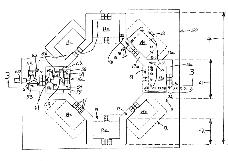
A ~ual frequency coil pair 10 accordiny to the invention
includes first and second individual coils 11 and 12 arranged
overlyin~ and in close proximity to one another. Each coil 11
and 12 is modeled in Fig. 1 as comprlsing conduc~i~e l.oops 13
and 14, with gaps 15 and 16 breaking each loop 13 and 14,
respectively. As is known in the art, the conducti~e loops 13
25 la~d 14 act as lnductive elements and discrete capacitors
represented at 17 and 18 may be added in para}lel with the gaps
15 and 16 acting as capacitive elements to form an L-C resonant
~ 2 2 ~ ~ 15NM03484
circuit for determining the resonant frequency of each coil 11
and 12, respectively. As is also known in the art, multiple
gaps and parallel capacitors may be distributed around the
conductive loops, although the Fig. l model is based on a
single gap/capacitor for simplicity of illustration. The
multiple gap/capacitor case is shown in the detailed
embodiments discussed below. Output leads 19 and 20 are
connected across the g~ps 15 and 17 to conduct the coil output
to a receiver for processing in the normal manner.
Different net values are utilized for the capacitors 15
and 16 so as to make the coi}s ll and 12 resonant at two
different frequencies. For example, coil ll may be made
resonant at approximately 26 MHZ for performing NMR
spectroscopy on phosphorous nuclei (31p), while coil 12 may be
made resonant at approximately 64 MHZ for imaging protons ~lH
nuclei~, assuming a polari~ing magnetic field (Bo) of 1.5
Tesla. Alternately, the coils 11 and 12 may be ~uned for any
specif~c nucle.i o~ interest for either imaging o~ spectroscopy.
The desirability of such a dual frequency coll is dlscussed
2~ abo~e in the background of the ~n~entio~. However the dual
frequency coLl pair according to the invention is able to
achieve the desired dual frequancy operatlon w~thout the
degradation of coll Q and signal to noise ratio ~SNR)
experienced in prior dual frequency coil pairs. The principle
according to the invention u~ilized to achieve that result,
which is described in detail below, is a specific structure and
arrangement for the coils 11 and 12 so as to minimize mutual
loading between them, even though they are essentially co-
planar with an almost identical field of view.
The conductive loops 13 and 14 each follow a serpentine
path, alternating between outer perimeter conductors 13a and
14a and inner perimeter conductors 13b and ~4b, with crossover
~conductors 13c and 14c connecting the outer perimeter
conductors 13a and 14a to the inner perimeter conductors 13b
and 14b, respective}y. As a result, the perimeter of each
~ ~ ~ 2 ~ 15NM034~4
conductive loop 13 and 14 defines an area which can be
considered to comprise inner areas 13d and 14d, and outer
areas, or "lobes~ 13e and 14e, respectively.
Since the firs~ and second coils ll and 12 are arranged
overlying and in clos proximity to each other, the conductive
loops 13 and 14 are separated by at most a small displacement
so as to maintain electrical isol~lon between them. As a
result, both coils 11 and 12 will exhib:Lt almost exactly the
same field of view. Further, the conductive loops 13 and 14
are formed so as to result in inner areas 13d and 14d,
respectively, which are essentially the same shape and
overlying one another. Consequently, magnetic flux coupling to
eit~er of the areas 13d or 14d will also couple nearly
completPly with the other area 14d or 13d, respectively. Even
though the conducti~e loops 13 and 14 may be displaced from
each other by a small amount, when the areas 13d and 14d are
arranged over each other as shown, the difference in ~lux
linkage between them is negliglble.
~n important principle of the invention ls that the coils
11 and 12 are arranged with the lobes 13e and 14e Lnterleaved
such that there is minimal overlap between the lobes 13e and
14e. In that way, resonant current circulating in one ,of the
coils 11 or 12 will produce a maqnetic field which does not
produce any significant loading by the other coil 12 or 11,
respecti~ely. A detailed explanation of this "unloadlngl'
phenomenon is presented below in the description of Fig. 2.
Preferably, the required interleaving is achie~ed by forming
both conductive loops 13 and 14 with an identical shape, and
then rotating the loops 13 and 14 with respect to each other.
In the preferred embodiments described herein, each coil 11 and
12 is formed with four lobes 13e and 14e, respectively, so that
, af45 relati~e ro~ation between the coils 11 and 12 will result
in the desired interleaving, as shown in Fig. 1.
Referring to Fig. ~, the effect of interleaving the lobes
13e and 14e is as follows. Currents in the conductive loops 13
2~2~ 15NM03484
--8--
and 14 produce magnetic fields in each respective current path
which encircle each respective current path according to the
right hand rule. For the sake of illustration, a sample
current in coil 11 is represented by arrow 30, with the
resultant circular magnetic fields being represented by
distributions 33-35, respectlvely. The magnetic field
dis~ributions 33-35 are shown as "X's" Eor field lines going
into the drawing and dotted circles for field lines coming out
of the drawing. It should be understood that since the current
30 is the same magnitude a~ all points in coil 12, the
resultant distributions 33-35 are also approximately equal in
magn~tude, but with the differing orientations as shown. It is
further understood that the actual coil currents are radio
frequency (~F~ alternating currents ~AC), so that the static
representations used herein can be considered phasor
representations o~ the actual RF AC currents, and that the
field denslty due to currents in any conductor is greatest near
the conductor, and diminishes with transverse d~stance away
from the cond~ctor, as lndicated by the spacing between the
indi~idual X's and dotted circle~.
The field distribu~ions 33-35 will induce localized
currents in the other coil 12 in a such a way that the net
effect is a composite current in coil 12 which is very near or
equal to zero. Speciflcally, the flux 33 and 34 wil} tend to
induce a localized current 31 in coil 12 in a "clockwise"
directlo~ arou~d coll 12, while at ~he same time the flux
distribution represented at 34 and 35 will tend to induce a
localized current 32 in coil 12 in the opposite, or counter-
clockwise direction. Opposed current pairs similar to those
represented at 31 and 32 occur all around coil 12, with the
effect ~hat the opposed currents tend to "buck", or cancel each
oth~r. It is further poss~ble ~o adjust the magnitude of the
'localized currents, particularly the outer current 32, by
appropriate modifications of the dimensions for the lobes 13e
35 and 14e. By arranging fbr the localized currents 31 and 32 to
2!3~22~ lSNM03~84
be approximately equal in ~agnitude, the currents 31 and 32 are
forced to remain localized, with negligible net, or aggregate
curr~nt. Due to the symmetrical layout of the coils ll and 12,
the above analy~is is equa}ly applicable to the opposite case
of considering the coupling of currents in currents in coiL 12
to coil 11. As a result each coil may operate at its own
separate resonant frequency with negligible loading or loss by
the other coil. In essence, the other coil appears to be
"invisible" from an electromagnetic coupling viewpoint.
Still referring to Fig. 2, a particular geometry for the
pres~ntly preferred embodiment which has proven to be
especlally effective tn practice is for each c~il 11 and 12 to
include ~our approxlma~ely recta~ular lobes ~ositloned at 90
intervals, with the distance between the outer edgas of
opposi~e lobes ~represented by 40 in Fig. 2) being
approximately five inches, with the width of each lobe.
(represented by 41) belng approximately 1.5 inches, and with
the length of each crossover conductor which defines the length
of each lobe ~represented by 42) being approximately one inch.
The conductive loops 13 and 14 in the Fig. 2 embodiment
are formed as copper traces approximately l/4 inch wide etched
on opposite side o~ a double sided printed circuit board 50
Multiple gaps 15 and 16, with multiple parallel capacitors 18
and 19, respectively, are used with each coiL 1} and 12. The
use of multiple series capacitors is well known in the art as a
means to reduce the effects of stray capacitance, since each
individual series capacitqr will have a lar~er value with
~réspect to stray capacitances than would a single lumped
capacitance of equal value. For example, coil 11 in this
embodiment (on the top surface of printed clrcuit board 50) is
2 ~ sNMo3484
-10--
tuned to a frequency of approximately 64 MHZ for imaging
protons ( 1H), while the bottom coil 12 is tuned to a frequency
of approximat~ly 26 MHZ for performing spectroscopy on
phosphorus nuclei (31p). Due to the higher resonant frequency
of the proton coil 11, a lower value of net capacltance is
required. Consequently, coil 11 includes a larger number of
gaps 14 and capacitors 18, so that the net capacitance can be
reduced while still usins capacitors 18 having relativeLy large
individual values. Relat~vely fewer gaps 15 and cap~citors 19
are required for the low~r frequency phosphorus coil 12. The
gaps lS and 16 àre formed as a part of the etching process for
the conductive loops 13 and 14. The capacitors 18 and 19 are
ceramic chip capacitors with flat conductlve strip tails shown
e.g. at 51. The capacitor tails 51 are soldered across the
lS gaps 15 and 16 so as to electrically connect the capacitors 18
and 19 in parallel with the gaps 15 and lÇ, respectively.
Referr~ng to Figs. 2 and 3, one of the gaps lSa and 16a
in each coll 11 and 12, respec~i~ely, is used to tap off an
output signal for connec~ion to a suitab}e receiver circuit
(not shown). ~n extra copper trace 53 and 54 is extended from
each loop 13 and 14, and copper pads 55 and 56 are provided, to
facilitate connection of external components 60-65 ~o the loops
13 and 14, respec~lvely. In the case of loop 14 ~hlch is
formed on the opposite side of the circuit board 50, a plated
through hole 57 ls used to connect the trace extension 54 to
the loop 14, and a second pad 58 is connected by a another
plated through hole 59 to the loop 14, thereby allowing the
external components 60-65 to all be mounted on the same side of
the circuit board S0. Specifically, the external components
include coaxial cable connectors 60 and 61, discrete series
load~ng inductors 62 and 63, and PIN diodes 64 and 65. Coaxial
cable connectors 60 and 61, have one connection soldered to
~trace extensions 53 and 54, while the other connection is
soldered to pads 55 and 56, respecti~ely. Series loading
inductors 60 and 61 are tonnected from pads 55 and 56 to a
2 ~ 4 2 ~ 15N~I03484
--11--
point on the conductive loops 13 and 14 on the opposite side of
the gaps 15a and 16a from ~race extensions 53 and 54,
respectively. The series loading inductors 62 and 63 are used
connect the coil outputs obtained across the gaps 15a and 16a
to the respective cable connectors 60 and 61, while at the same
time matching the impedance of the respective coils 11 a~d 12
to the impedance seen at the receiver cables (not shown). ~N
diodes 64 and 65 are connected from trace extensions 53 and 54
to pads S5 and 56, respecti~ely, and are used to clamp the coil
outputs when a transmit field is applied by an external
transmit coil (not shown). When switched on by the application
of an external DC current, the PIN diodes 64 and 6S in
conjunction with capacitors 15a and 16a, and coils 62 and 63,
present an increased impedance in coils 11 and 12, so as to
lS limit generation of extraneous magnetic fields by coils 11 and
12 to in turn preven~ loading and distortlon of the transmit
field.
Another important teaching of this invention is that the
above described ability of the coils 11 and 12 to opera~e
independently is preserved even if ~he coil pair is cur~ed,
i.e. other than in a fla~ plane. T~e abo~e descri~ed effects
which l~rgely prevent mutual lading between the coils 11 and 12
: is still exhlbited when the coils 11 and 12 are curved out of a
flat plane. Flexible coils are advantageou~ in that they may
be conformed to an area of interest, for example, when
performlng an NMR study on a l~mb of a human patlent. It is
therefore contemplated by the invention that the prlnted
circult board 50 may be a flexible typ~ of printed circuit
board material, or other flexible substrate for supporting the
coils 11 and 12.
Re~erring to Fig. 4, a second preferred embodiment of the
invention is specifically adapted to permit flexing of the
~c~ils 11 and 12. In this case, the coils ll and 12 are split
between two separate supportlng str~ttures, or substrates 70
and 71. In the preferre~ form, the substrates 70 and 71 are
~ 2 :~ ~ 15NM03484
-12-
each a piece of rigid, fiberglass-epoxy double sided printed
circuit board material. Although the preferred substrates 70
and 71 are rigid, it should be apparent to those ~killed in the
art that flexible substrates could also be used.
Each of the printed circuit boards 70 and 71 is formed
with a portion of each conductive loop 13 and 14, and the
boards 70 and 71 are spaced apart from one another with respect
to an axis sho~n by dotted line 73 in Fig. 4. A set of
flexible, metallic phosphor-bronze jumpPr strips 75-78 are used
to connect the s~parate conducti~e loop portions across the
sep~ratton between the printed circui board~ 70 and 71. As a
result, the circuit boards 70 and 71, although individually
rigid, can be flexed with respect to each othex with the
flexible ~umper strips 75-7~ acting in effect as a hinge.
The jumpers 75-78 are preferably all attached on the same
slde of the circu~t boards 70 and 71, and are attached using
r~vets 80 through plated-through holes formed in the printed
circuit boards. Jumpers 76 and 77 orm two o~ the in~er
perimeter conductors for the loop 13 on the top slde of the
printed circuit boards 70 and 71. The copper traces forming
the loop 13 on the circuit boards 70 and 71 are continued under
the jumpers 76 and 77 all the way to the ed~e o~ the respective
boards 70 and 71 to insure good electrical contact between the
traces and the jumpers 76 and 77.
Ju~pers 75 and 78 are used to complete the other
conductive loop 14 for coil 12. The copper traces for loop 14
however are on the other side of boards 70 and 71. To aid in
the electrical contact between the traces for loop 14 and the
jumpers 75 and 78, copper pads ~not visible in Fig. 4) are
formed on the top of circuit boards 70 and 71 underneath the
area covered by ~he jumpers 75 and 78 on circuit boards 70 and
71. The underlying pads 3re electrically connected to the
traces on the opposite side of the boards 70 and 71 by the
plated through holes for the riYets 80. Soldering of the
jumpers 75-78 to ~heir respective traces may also be performed
2 1 ~
15NM03484
-13-
to improve the electrical contact therebetween.
In addition to the advantage of flexibility, the split
circuit boards 70 and 71 in the Fig. 4 embodiment also have the
advantage that an opening, outlined by dotted line 82, is
in~roduced in the interior of the coil pair 10. The coil pair
10 may be contained within a protective housing, which itself
may be hinged or otherwise fle~ible, and the protective housing
may also contain an opening coinciding with the opening 83.
Since the opening 83 is at the geometric center of the coil
pair 10, it allows direct visual observation of the area in the
primary field of vlew of the coll pair 10. This is of great
benefit in positioning the coil pair 10 at a precise area of
intarest on a human patient or other sample.
Still referring to Fig. 4, since the jumpers 75-78 are
solid metalLic strips, it would not be practical to introduce
gaps therein. Instead, the gaps which would otherwise occur
across ~he jumpers 75-78 may be relocated to other portions of
the loops 13 and 14, with appropriate ad~ustment of the
capacitance values. In all other respects, the Fig. 4
embodiment is similar in operation to the embodiment of F~gs.
21 and 3 described above.
Numerous modlfications to the above described embodiments
within the scope of this invention would be apparent ~o those
skilled in the art. For example, trimming components in the
form of fixed or varlable inductors or capacitors may be added
at app~oprlate points ln either or both of the coils in the
coil pai~ to fine tune the exact frequency of resonance.
Additionally, it should be observed that the colls in the coil
pair may be placed so close togethex, with respect to their are
of coverage, that the individual coils may be considered
essentially co-planar. In fact, it is possible according to
the in~ention to actually make ~he individual coils co-planar,
with only ~umpers across the poin~s where the individual coils
cross over each other. Another possible modification is to
form ~he area corresponding to each lobe from multiple turns of
2 ~,rl~2 ~ ~
1~NM03484
-14-
the conductive loop, although this approach introduces more
loss and generally inferior performance to the single turn lobe
embodiments described above. Finally, it should be apparent
that the Lobes themselves may be formed in a variety of shapes
in addition to the above described rectangular lobes, and that
any number of lobes may be used. For example, five or six
lobed colls may be practical, but it may be difficuLt to
achieve complete cancellation with too many or too few lobes.
Further, the individual lobe shapes may be multi-sided or even
rounded, provtded that the lobes between the indi~idual coils
are interleaved wi~h respect to each other and encompass an
area su~icient to achieve the desired cancellatlon.