Note: Descriptions are shown in the official language in which they were submitted.
1- 20~2274
RD-20,025
pT~--Q~I~UT, S~NG~ ND~- R~SO~
POWTR CONV~T~
F~el~ of th~ I~v~inn
The present invention relates generally to DC-to-DC
power converters. More particularly, the present invention
relates to a high-frequency, single-ended, resonant converter
which provides a main output DC voltage, which may be
constant or variable, and multiple auxiliary regulated output
voltages.
sack~rou~d of the I~ventiQn
A single-ended, resonant power converter is
described in Steigerwald U.S. Patent No. 4,845,605, issued
July 4, 1989, which patent is assigned to the instant
assignee and is incorporated herein by reference. The
converter of the Steigerwald patent is capable of operating
at high frequenciec~ e.g. 1 MHz, and achieving high power
densities. Furthermore, zero-voltage switching is realized
by the Steigerwald converter, resulting in highly efficient
converter operation.
One way to obtain multiple output voltages from a
DC-to-DC power converter, such as the aforementioned single-
ended, resonant converter, is to provide additional windings
on the output transformer. In order to obtain regulated
output voltage~, however, a high degree of coupling among all
transformer windings is essential. At high frequencies,
tight coupling is difficult to achieve, resulting in output
voltages which do not track closely. ~oreover, if the main
output winding is short-circuited, or if the main output
winding is used to provide a variable voltage, then the
auxiliary output voltages cannot be regulated because they
track the main output voltage by virtue of the transformer
coupling. Hence, it is desirable to provide a regulated
- 2 _ 2 0 ~ 22 7~
RD-20,025
power supply with multiple auxiliary output voltages that are
independent of the main output voltage, which power converter
is sufficiently simple in construction in order to be
practicable for widespread applications.
s
Accordingly, an object of the present invention is
to provide a new and improved single-ended, high-frequency,
resonant power converter which is capable of providing
multiple regulated output voltages.
Another object of the present invention is to
provide a single-ended, resonant power converter which is
capable of providing a variable main output voltage and
multiple auxiliary regulated outpu~ voltages which are
independent of the main output voltage.
Still another object of the present invention is to
provide a regulated power supply which has multiple outputs
and is simple in construction.
Yet another ob~ect of the present invention is to
provide a single-ended, resonant power converter which is
capable of providing multiple regulated, auxiliary output
voltages independent of the converter switching frequency.
S~mary of the Invent1gn
The foregoing and other objects of the present
invention are achieved in a high-frequency, single-ended,
resonant power converter capable of providing multiple
regulated output voltages. The single-ended, resonant
converter comprises a single, primary-side power switching
device coupled to a resonant circuit which includes a
capacitor, an inductor, and the parasitic capacitance of the
power switching device. In accordance with the present
inventlon, an input filter inductor has a primary winding and
multiple auxiliary, or secondary, windings. When the power
~`` - 3 - 20~227~
RD-20,025
switching device is conducting, an input DC voltage is
applied to the input inductor so that the voltage across the
input inductor (which is substantially equal to the input DC
voltage) is transformed directly to the auxiliary windings.
The voltage across each auxiliary winding is rectified by a
corresponding output diode. A filter capacitor is coupled to
each output diode for maintaining the respective voltage
applied thereto when the power switching device is turned
off. As a result, the converter provides multiple auxiliary,
regulated output voltages in addition to the main converter
output DC voltage. Advantageously, these auxiliary output
voltages are a function of the input voltage only and are not
a function of the main output voltage of the converter.
Hence, the converter provides the multiple regulated,
auxiliary output voltages even if the main output voltage is
variable. The converter of the present invention is
particularly suitable for applications wherein the input
voltage is fully or semi- regulated, such as distributed
power applications, e.g. satellite systems, radar systems,
and distributed computing systems, because the auxiliary
ou~put voltages, which are directly proportional to the input
DC voltage, are approximately as well regulated as the input
voltage.
The single-ended, resonant power converter of the
present invention is advantageously highly efficient. First,
zero-voltage switching of the power switching device is
maintained by the resonant action of ~he main power circuit.
In addition, power to the auxiliary converter outputs is not
transferred through the resonant circuit elements.
As another advantage, the high frequency, single-
ended, resonant powPr converter of the present invention is
simple in construction. In particular, to obtain multiple,
regulated auxiliary output voltages from a single-ended,
resonant power converter, such as the Steigerwald converter
- 4 - 2 0 4 22 7 ~
RD-20,025
hereinabove discussed, the only additional elements required
are auxiliary secondary windings on the input inductor, and
an output diode and filter capacitor per auxiliary output.
Brlef D~.SG~i~tio~Q~-~hQ-~io~5
The features and advantages of the present
invention will become apparent from the following detailed
description of the invention when read with the accompanying
drawings in which:
Figure 1 is a schematic diagram of a single-ended
resonant DC-to-DC power converter of the prior art;
Figure 2 is a schematic diagram of a multiple-
output, single-ended, resonant DC-to-DC power converter in
accordance with a preferred embodiment of the present
invention; and
Figure 3 is a schematic diagram of a multiple-
output, single-ended, resonant DC-to-DC power converter in
accordance with an alternative embodiment of the present
invention.
Figure 1 illustrates a single-ended, resonant, DC-
to-DC power converter lO, such as that described in
Steigerwald U.S. Patent No. 4,845,605, cited hereinabove. An
input filter inductor Ll receives an input DC voltage VIN-
Inductor L1 is coupled to a single power switching device Ql-
Power switching device Ql is illustrated in Figure 1 as
comprising a power MOSFET having a drain electrode connected
to inductor L1 and a source electrode connected to the
circuit common. Switching device Q1 also includes a
parasitic output capacitance, represented by capacitance Cq,
and a parasitic anti-parallel diode, represented by diode Dq.
A main resonant power circuit ll, including a resonant
circuit 12, is coupled in parallel with switching device Ql
_ 5 _ 2 0 4 227 ~
RD-20,025
at the junction between inductor Ll and switching device Ql to
complete the converter. The resonant circuit 12 includes the
series combination of a DC blocking capacitor Cb, a resonant
inductor Lr~ and another capacitor Cd. The resonant circuit
further includes parasitic capacitance Cq when switching
device Ql is turned off. The primary winding 14 of an output
transformer To is connected in parallei with capacitor Cd.
Secondary windings 16 and 18 are connected together at a
center tap terminal 20, with the remaining end of each
secondary winding 16 and 20 being connected, respectively, to
the anode of a rectifying diode D1 and D2, respectively. The
cathodes of diodes Dl and D2 are connected to each other and
further to an input terminal of an output filter inductor Lo.
The other terminal of output filter inductor Lo is coupled to
an output filter capacitor COI the other terminal of which is
connected to the transformer center tap terminal. A control
circuit 22, such as the one described in the Steigerwald
patent, cited hereinabove, is coupled to the gate electrode
of switching device Ql for controlling the conduction
interval thereof in order to adjust and regulate the
converter output voltage VOUT-
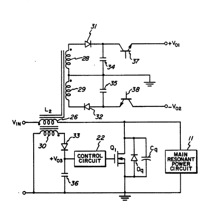
Figure 2 illustrates the portion of a preferredembodiment of a multiple output, single-ended, resonant, DC-
to-DC converter of the present invention. An input filter
inductor L2 includes a primary winding 26 and multiple
auxiliary, or secondary, windings 28-30. For illustrative
purpo~es, three secondary windings are shown in the
embodiment of Eigure 2. Each secondary winding 28-30 is
coupled in series with a diode 31-33, respectively, and a
filter capacitor 39-36, respectively. Furthermore, to obtain
an even higher degree of voltage regulation, a series pass
regulator of a type well-known in the art may be employed to
receive the respective output voltages at the junctions
between the corresponding series combination of the diode and
- 6 - 2~227 ~
RD-20,025
filter capacitor. For example, series pass regulators 37 and
38 are shown in Figure 2 as being coupled to capacitors 34
and 35, respectively. Suitable series pass regulators may
comprise semiconductor devices, such as the 7800 series of
monolithic voltage regulators manufactured by Motorola, Inc.,
National Semiconductor Corporation, and others.
In operation, when switching device Q1 is on, i.e.
conducting, the DC input voltage VIN is applied directly to
the input inductor L2. Hence, this voltage is transformed
directly to secondary windings 28-30 and rectified by diodes
31-33. As a result, the output voltages vOl-v03 are directly
proportional to the input voltage VIN. When Q1 is turned off,
filter capacitors 34-36 maintain the output voltages VO1-V03,
respectively. Advantageously, therefore, the output voltages
Vol-VO3 are independent of the switching frequency of device
Q1, which controls the main output voltage VOUT of the
converter. Moreover, if desired, one of the output voltages
VOl-V03 may be coupled to control circuit 22 for providing
regulated power thereto. For example, the output voltage V03
at the junction between diode 33 and capacitor 36 is shown as
being coupled to control circuit 22 (Figure l).
As another advantage of the present invention, the
output voltages Vol-VO3 are approximately as well regulated as
the input voltage VIN. Furthermore, as explained hereinabove,
if an even higher degree of regulation of the output voltages
VOl-V03 is deslred, then series pass regulators may be
employed, such as regulators 37 and 38 illustrated in Figure
2. Fortunately, the power dissipation of such series
regulators is generally low due to the substantially
regulated input voltage VIN-
As still another advantage of the power converterof the present invention, the auxiliary output voltages VOl-
Vo3 are not functions of the main output voltage VouT~ which
is controlled by the switching frequency of switching device
- 7 - 2 0 4 22 7 4
RD-20,025
Ql- In particular, the auxiliary output voltages VO1-V03 are
only dependent upon the input voltage VIN. Hence, efficient,
regulated auxiliary output voltages Vol-VO3 are maintained
even if the main output voltage VO~T is variable.
S Yet another advantage of the power converter of the
present invention is high-efficiency operation. First of
all, zero-voltage switching of switching device Ql is
maintained due to the resonant action of resonant circuit 12
as described in Steigerwald U.S. Patent No. 4,845,605, cited
hereinabove. Secondly, auxiliary output power for providing
the multiple auxiliary output voltages VOl-V03 is not
transferred through the resonant circuit elements.
Figure 3 illustrates an alternative embodiment of
the portion of a power converter according to the present
invention wherein input inductor L3 comprises a combination
differential-mode/common-mode choke having two coupled
primary windings 40 and 42. In such case, the input voltage
VIN iS ideally divided equally between the two primary
windings 40 and 42 of choke L3 when switching device Ql is
turned on. (In practice, however, the voltage does not
divide exactly equally due to slight differences in the
inductances of windings 40 and 42). Choke L3 further
comprises multiple secondary windings, shown in Figure 3 as
secondary windings 44-48. Each secondary winding 44-48 is
coupled in series with a rectifying diode 50-54,
respectively, which in turn is coupled to a capacitor 56-60,
respectively, for maintaining the auxiliary output voltages
VO1-Vos when switching device Q1 is turned off.
Advantageously, the auxiliary output voltages Vol-vos are
independent of the main output voltage VouT and the converter
switching frequency and are approximately as well regulated
as the input voltage VIN. Moreover, if desired, one of the
multiple auxiliary output voltages, e.g. voltage VOs, may be
- 8 - 2 ~ ~22~ ~
RD-20,025
coupled to control circuit 22 (Figure 2) for providing
control power thereto.
While the preferred embodiments of the present
invention have been shown and described herein, it will be
obvious that such embodiments are provided by way of example
only. Numerous variations, changes and substitutions will
occur to those of skill in the art without departing from the
invention herein. Accordingly, it is intended that the
invention be limited only by the spirit and scope of the
appended claims.