Note: Descriptions are shown in the official language in which they were submitted.
2~42~2,~
GLOBAL POSITIONING SYSTEM RECEIVER
Background of the Invention
This invention relates to digital signal processing
for both radar and communications using phase code
modulation, and in particular to an apparatus and method
for correlating Binary Phase-Shift Keying (BPSK) pseudo-
random noise (PN) codes in a signal processor of a
Global Positioning System (GPS) receiver.
Phase code modulation is ideally suited to measuring
time or time delay. The time delay is a measure of range
while the difference in phase measurements taken at fixed
time intervals is a measure of frequency. The phas~ code
modulation is compared (correlated) with the expected phase
or replica of the phase code modulation. Typical phase
code modulations include not only Binary Phase-Shift: Keying
(BPSK), but also Binary Frequency-Shift Keying (BFSE~).
The Global Positioning System (GPS) is a navigation
system based on eighteen satellites in orbit. When fully
operational the eighteen satellites will be evenly dispersed
in three, inclined, 12-hour circular orbits chosen l:o ensure
continuous 24-hour coverage. The GPS will provide extremely
accurate time and three-dimensional position and veLocity
information to users anywhere in the world. NormalLy,
four satellites are required for precise location determin-
mination in four dimensions (latitude, longitude, altitude
and time). The location determinations are based on
measurement of the transit time of RF signals from the
satellites selected from the total of eighteen. Each
satellite transmits a different pair of L-band carrier
signals including an Ll signal at 1575.42 MHz and an L2
signal at 1227.6 MHz. The Ll and L2 signals are biphase
modulated by two pseudo-random noise (PN) codes ccmprising
a P-code which provides for precision measurement of
transit time and a C/A (course/acquisition) code which
provides for a course measurement of transit time and
provides for easy lock-on to the desired signal suitable
for many commercial purposes. Since each satellite
uses different PN-codes, a signal transmitted by al
particular satellite can be selected by generating and
matching (correlating) the corresponding PN-code pattern.
The P-code is the principal navigation pseudo-random
noise (PN) ranging code of the Global Positioning System.
The P-code is a repetitive sequence of bits referred to as
chips (in spread spectrum parlance). The P-code for each
satellite is the product of two PN-codes Xl and X,' where
Xl has a period of 1.5 sec or 15,345,000 chips ancl X2
has a period of 15,345,037 or 37 chips longer. The
P-code generator in a GPS receiver reproduces a replica
of the P-code that is generated by a P-code generator
of a particular GPS satellite and each satellite
2 ~ 4 ,~
produces a unique P-code. The C/A code is a relatively
short code of 1023 bits or 1 msec duration at a 1.023
Mbps bit rate. This code is selected to provide good
multiple access properties for its period.
An all-digital GPS receiver is described in a paper
entitled "All-Digital GPS Receiver Mechanization", by Peter
C. Ould and Robert J. Van Wechel, reprinted by the Institute
of Navigation, Global Positioning System Papers published in
Navigation, Vol. 2, pp. 25-35, (also presented at ION
Aerospace Meeting, April, 1981). Code correlation is
accomplished digitally using either digital matched
filters (DMF) or digital correlators, depending uFon
performance requirements. In particular, a correlator
is described that is a three-sample, 2-bit correlator
used for both C/A and P-codes wherein the quantized
samples are scaled to produce all positive values so
that simple up/down counters can be used to integrate
the most significant bit (MSB) and least significant
bit (LSB) independently. However, this approach requires
one correlator/integrator in the signal processor of
the GPS receiver for each analog-to-digital bit. In a
subsequent paper entitled "All-Digital GPS Receiver
Mechanization-Six Years Later by J.S. Graham, P.C. Ould
and R.J. Van Wechel, Journal of Institute of Navic~ation,
National Technical Meeting, January 1987, a multi-tap
~Yl.~252~
correlator/integrator is described that is predominantly
a set of N times Y 16-bit up/down counters where N is
the number of A/D bits and Y is the multiple number of
taps. When sampled signals are correlated against a
replica of the transmitted code, the counters count up
or down to indicate a match or mismatch, respectively
for each A/D bit. At the end of the correlation time
interval the counts for each A/D bit are stored in
holding registers accessible by a microprocessor bus.
This integrate and dump function which is the optimal
filter requires weighting of each 16-bit up/down counter
output. The N 16-bit output weighted words are accumulated
for detection of pseudo-random noise code buried in
Gaussian noise. However, these approaches for pseudo-random
noise code correlation result in considerable harclware
even when implemented with VLSI circuitry.
New applications of the GPS system have ident:ified
the need for a GPS receiver having a signal processor
implemented on a very large scale integrated (VLS]:)
circuit. In order to accomplish this level of int:egration,
the signal processor has to be designed with minimum
circuitry to facilitate implementing it on a VLSI
circuit.
Summary of the Invention
Accordingly, it is therefore an object of this
invention to provide a GPS receiver to perform N-bit
correlation of a received PN-code modulated carrier
with sign and magnitude input weighting.
It is another object of this invention to provide
a GPS receiver which performs N-bit correlation of a
received PN-code modulated carrier using minimum circuits
and interconnections to facilitate very large scale
integrated (VLSI) circuit implementation.
It is a further object of this invention to provide
a PN-code correlation apparatus for a GPS receiver which
generates a PN-code reference to provide both an in-phase
reference (IREF) signal and quadrature-phase reference
(QREF) signal to enable performing either IF sampling
or baseband sampling of the received PN-code modulated
carrier.
It is a further object of this invention to provide
a multi-channel signal processor wherein each channel
comprises a sign and magnitude input weighted correlator
for correlating BPSK pseudo-random noise codes.
The objects are further accomplished by a Global
Positioning System (GPS) receiver comprising a GP',
receiver front end for performing sampling of a received
PN-code modulated carrier to generate in-phase (I) and
204~'522
quadrature-phase (Q) samples, a signal processor coupled to
outputs of the receiver front end for removing a doppler
frequency and PN-code modulation from the modulated carrier,
the signal processor comprises a plurality of channels, each
of the channels including a correlator means, having a sign
and magnitude input weighting, for correlating the I and Q
samples with in-phase ( IREF) and quadrature-phase (Q:REF)
components of an internally generated PN-code reference, the
correlator means controlled in response to a weighting select
signal, and means coupled to the signal processor for
processing the correlated I and Q samples. Preferably, the
means for processing the correlated I and Q samples comprises
means to provide multi-channel control signals to the signal
processor and to estimate a pseudo-range and a pseudo-range
rate.
Preferably, the GPS front end receiver comprises
either IF sampling or baseband sampling for generating said I
and Q samples. For baseband sampling the correlator
preferably comprises means for correlating the I and Q samples
with only the IREF component of the internally generated PN-
code reference. The sign and rnagnitude input weighting of the
correlator comprises register rneans for storing an R factor
weighting input, multiplexor means coupled to the register
means for selecting between weighted inside crossings of the
samples and weighted outside crossings of the samples in
accordance with the weighting select signal, and log:Lc means
coupled to the multiplexor for generating the weight:ing select
signal in accordance with sign and magnitude inputs of the
-- 6
62901-759
' 1'~
2l)42~)22
samples to the logic means.
The objects are further accomplished by a
correlation apparatus comprising means for removing :received
carrier doppler from in-phase (I) and quadrature-phase (Q)
samples of a received pseudo-random noise (PN) code modulated
carrier signal, means coupled to the received carrie;r doppler
removing means for generating a PN-code reference wh:Lch is a
replica of the received PN-code, the PN-code reference having
an in-phase ( IREF) component and a quadrature-phase (QREF)
component, and means, coupled to the carrier doppler removing
means and the PN-code reference replica generating means, for
correlating the I and Q samples with the IREF and QREF
components respectively of the replicated PN-code. The
correlating means preferably comprises sign and magn:Ltude
input weighting means of the I and Q samples. The input
weighting prepferably applies an R weighting factor t:o the
samples thereby providing the weighted samples with additional
A/D conversion gain for correlation, adder control means
coupled to the input weighting means for determining whether
each of the weighted samples is added to or
'B 62901-759
".
subtracted from an accumulated value of the weighted
samples in accordance with a correlator control signal,
means for ge~erating the correlator control signal by
comparing a sign of the sample to the PN-code reference
signal, and integrator means coupled to the adder
control means and the correlator control signal generating
means for accumulating and integrating the weighted
samples over a correlation time interval. The R factor
weighting input for outside crossings is variable under
programmed control or may be a constant for a speciiric
correlation interval (Tcj)~
The objects are further accomplished by a method
for performing PN-code correlation in a Global Posilioning
System receiver comprising the steps of sampling a
received PN-code modulated carrier in a GPS receiver
front end to generate in-phase (I) and quadrature-phase
(Q) samples, removing a doppler frequency and PN-code
modulation from the modulated carrier in a signal
processor, the signal processor comprises a plurality
of channels, each of the channels including a corre.lator
means having sign and magnitude input weighting,
correlating in the correlator means the weighted I and
Q samples with in-phase (IREF~ and a quadrature-pha;e
(QREF) components of an internally generated PN-code
reference, and processing the correlated I and Q samples
in a processor means. 2 (:~ 4 2 Jl 2 2
Preferably, the step of sampling in the GPS receiver
front end comprises the step of performing IF sampling or
baseband sampling for generating said I and Q samples.
Preferably, the step of performing baseband sampling further
comprises the step of correlating the weighted I and Q samples
with only the IREF component of the internally generated PN-
code reference.
The objects are further accomplished by a method of
performing correlation comprising the steps of: removing
received carrier doppler from in-phase (I) and quadrature-
phase (Q) samples of a received pseudo-random noise (PN) code
modulated carrier signali generating a PN-code reference which
is a replica of said received PN-code, said PN-code reference
having an in-phase ( IREF) component and a quadrature-phase
(QREF) component; and correlating said I and Q samples with
said IREF and QREF components respectively of said replicated
PN-code.
62901-759
1~
Brief Description of the Drawings
Other and further features of the invention will
become apparent in connection with the accompanying
drawings wherein:
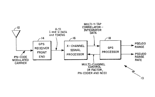
FIG. 1 is a block diagram of a Global Positioning
System receiver having an X-channel signal processor 16
comprising the invention;
FIG. 2 is a block diagram of an X-channel signal
processor comprising the multi-Y-tap correlator/integrator
nventlon;
FIG. 3 is a block diagram of one channel of an X-
channel signal processor showing the I multi-Y-tap
correlator/integrator and Q multi-Y-tap correlator/
integrator;
FIG. 4 is a timing diagram for the invention showing
I samples and Q samples alignment with a reference
code;
FIG. 5 is a logic block diagram of the I and Q
code reference generator shown in FIG. 3;
FIG. 6 is a functional block diagram of an I OI- Q
correlator/integrator tap having I or Q input weight:ing
for a 2-bit A/D;
FIG. 7 is a functional block diagram of an I or Q
correlator/integrator tap having input weighting for
an N-bit A/D;
-- 10 --
~ ; J ~. h
FIG. 8 is a block diagram of the invention comprising
an I eight-tap correlator/integrator;
FIG 9 is a block diagram of the invention comprising
a Q eight-tap correlator/integrator;
FIG. 10 is a logic block diagram of the I or Q
correlator coupled to the integrator;
FIG. llA is a logic diagram of the integrator showing
overflow control for the I or Q integrator;
FIG. llB is a timing diagram for the integrator
of the multi-Y-tap correlator/integrator showing the
time relationship of 2FSXN, a 1 ms correlation interval
(Tcj)~ and the delayed correlation interval timing pulses
TcjDXN(O) for tap O and TcjDXN(l) for tap l;
FIG. 12 is a logic diagram of one I or Q muilti-Y-tap
integrator overflow control coupled to an output register
which is shown in FIG. llA as the output register/overflow
control;
FIG. 13 shows the I or Q correlator 16-bit output
levels for one I or Q Y-tap.
Description of the Preferred Embodiment
Referring now to FIG. 1, there is shown a block
diagram of a Global Positioning System (GPS) receiver
10. The GPS receiver provides acquisition and tracking
of received Binary Phase Shift Keying (BPSK) modulated
carrier signals. The GPS receiver 10 comprises an
antenna 12 for receiving BPSK modulated carrier signals
and the antenna 12 is coupled to a GPS receiver front
end (RFE) 14 for performing RF/IF processing with
analog-to-digital (A/D) conversion in order to generate
in-phase (I) and quadrature-phase (Q) signal outputs.
The GPS RFE 14 also inc:ludes a receiver frequency
standard oscillator and timing synthesizer (not sh.own
but known to one skilled in the art) for generating the
GPS receiver 10 clocks and timing pulses. The Gpc RFE
14 outputs are coupled to an X-channel signal processor
16 which is used to acquire and track a plurality of
satellite vehicle transmitters. The maximum number of
channels is twelve which is determined by the number of
satellites in view at one time and the minimum number
is five with four required for estimating latitudc-~,
longitude, altitude, and time. The fifth is requi.red
to search the sky for determining the optimum set of
four satellites to be used for estimating latitude~,
longitude, altitude and time. The X-channel signal
- 12 -
~ 2 l~
processor 16 removes the BPSK pseudo-random noise code
modulated on the received RF carrier. The X-channel
signal processor 16 produces correlator/integrator data
which is coupled to a GPS processor 18 and the GPS
processor 18 generates an R factor, PN-coder and NCO
control signals which are fed back to the X-channel
signal processor 16. The GPS processor 18 tracks the
received RF carrier to remove the doppler frequency and
PN-code modulation in each signal processor channel.
The A/D I and Q data from the GPS RFE 14 is coupled to
a phase rotator in each channel of the X-channel signal
processor 16 for removal of received signal carrier
doppler. The GPS processor 18 estimates the pseudo
range and pseudo range rate of a GPS satellite.
Referring now to FIG. 2, a block diagram of the X-
channel signal processor 16 is shown comprising system
timing 20 means and a plurality of channels 221 to 22X,
each channel comprising the invention of an improved
multi-Y-tap correlator/integrator 241 to 24x. An input-
output interface 26 provides a serial output for the
multi-Y-tap correlator/integrator data which is fed to
the GPS processor 18 and such interface 26 receives via a
serial input an R factor control, PN-coder control and
NCO control signals for each channel from GPS processor 18.
Referring now to FIG. 3, a block diagram of one
2i,~,
X-channel 24X of the X-channel signal processor 16 is
shown comprising an I multi-Y-tap correlator/integrator
38 and a Q multi-Y-tap correlator/integrator 40. Each X-
channel receives timing signals which are coupled to a
timing signals buffer 30 for distribution within the
channel, and each X-channel receives I and Q data signals
from the GPS RFE 14. The A/D I and Q data signals are
coupled to a phase rotator 32 for removal of received
signal carrier doppler. The phase rotator 32 output in
each channel 22 is coupled to the Y-tap correlator/integrator
to remove the PN-code modulation for code and carrier
tracking in the GPS processor 18. The IouT and QOUT
from the phase rotator 32 are then fed to the I multi-Y-tap
correlator/integrator 38 and the Q multi-Y-tap correlator/
integrator 40 respectively where the I signal and Q signal
correlations strip-off the PN-code modulation for extended
range tracking in each channel. A numerical controlled
oscillator (NCO) clock signal from the timing signals
buffer 30 is coupled to a carrier NCO 44 and a code
NCO 46. The carrier NCO 44 produces five bits of the
most significant carrier NCO bits of the instantaneous
phase output (where each of the bits starting with
the most significant bit represents 180~, 90~, 45~,
37.5~ and 22.5~) and these 5 MSBs are coupled to the
phase rotator 32 for phase rotating the received I and
~2~t2~
Q data A/D samples. The limited number of carrier NCO
bits used for the phase rotator angle does not degrade
the phase resolution because the full precision estimates
are maintained in the GPS processor 18 shown in FIG. 1.
The correlated I and Q data from the I multi-Y-ta~
correlator/integrator 38 and the Q multi-Y-tap correlator/
integrator 40 in each channel is transmitted to the GPS
processor 18 at a one millisecond correlation interval
time (Tcj) over a serial output port 42. The code NCO 46
produces 6 bits of the most significant code NCO bits
of the instantaneous integer and fractional code chips
of delay or range and the most significant bit is 4
P-code (10.23 MHz) chips of delay. The 6 MSBs (re!present
4, 2, 1, 1/2, 1/4 and 1,/8 P-code chips of delay) are
coupled to the delay controller 34. The limited number
of code NCO bits used for the delay controller 34 does
not degrade fractional chips of delay or range resolution
because, as previously noted, the full precision estimates
are maintained in the GPS processor 18 shown in Fl:G. 1.
The 6 MSBs of the code NCO 46 are coupled to a delay
controller 34 to keep the received I and Q signals
centered within a particular correlator/integrator tap.
A 2FS sample clock and eight. 1/8 chip delayed Fo clocks
are coupled to the delay controller 34 along with a
signal from the code multipl.exor (MUX) 52. The output
~ i ~ f~~ ,~ ~ 2
of the delay controller 34 is a reference code which is
coupled to I and Q code reference generator 36. The I
and Q code reference generator 36 generates Y I-reference
code replica signals which are coupled to the I multi-Y-tap
correlator/integrator 38 and also generates Y Q-reference
code replica signals which are coupled to the Q multi-Y-tap
correlator/integrator 40 where Y is the number of taps
in the multi-Y-tap correlator/integrators 38, 40.
Still referring to FIG. 3, the Fo clock, which is the
local 10.23 MHz reference, is coupled from the timing
signals buffer 30 to a C/A coder 48 and P coder 50.
The C/A coder 48 generates a C/A code replica and the P-
coder 50 generates a P code replica. The C/A coder 48
and the P coder 50 generate a replica of the PN-code
modulated on the received RF carrier signal. The delayed
code replica is aligned with the received PN-code A/D
samples by the delay controller 34 which produces the REF
CODE signal. The C/A and P-codes are coupled to the
code multiplexor (MUX) 52 which selects the transfer of
such codes, and the output of code MUX 52 is a PN-code
which is fed to the delay controller 34 in accordance
with a coder control signal received from an input port
44. A PN-code chip is the time or period defined by
the PN-code frequency (1.023 MHz or 10.23 MHz for the
GPS receiver 10). The I and Q code reference tap
- 16 -
i 2 r~ 2 ,..
spacing is either 1/2 OI- 1 PN-code chip spacing, where
the PN-codes are C/A, P or E. The GPS C/A code is
1.023 MHz and P-code frequency is equal to the external
(E) code frequency 10.23 MHz. The input port 44 receives
control data from the GPS processor 18 for R factor,
C/A coder, P-coder and NCO control. The R factor
control data is coupled to the I multi-Y-tap correlator/
integrator 38 and the Q multi-Y-tap correlator/integrator
40. The coder control data is coupled to the C/A coder
48, P-coder 50 and a code multiplexor (MUX) 52. This
code control data from the input port 44 provides
control for acquisition, code and carrier tracking and
when applicable built-in-test capability. Such ccntrol
data is received from the GPS processor 18 at multiples
of a one-millisecond correlation interval for the
X-channel signal processor 16 to acquire and track up
to X satellites on C/A, P, or E-code where E-code is an
external replica of another code transmitted.
Referring now to FIGS. 4 and 5, FIG. 5 is a block
diagram of the I and Q code reference generator 36.
The timing relationship of the I-reference and Q-reference
code replica signals to the clock signals (4FS ancl 2FS)
are shown in FIG. 4. The reference code (REF. COOE)
signal shown in FIG. 3 and 5 is either ~or baseband A/D
sampling where I and Q samples are taken at the same
~ ~ ~ t~l 5 ~
instant in time or for IF sampling used in the present
embodiment where the I and Q samples are sequenced in
time through an in-phase A/D converter. IF sampling
uses only an in-phase analog-to-digital converter to
sample the IF signal at a number of quarter cycle
intervals as described in U.S. Patent Application
Serial No. 319,504, filed March 6, 1989 entitled "Spread
Spectrum Detector," by inventor Robert H. Cantwell and
assigned to the present assignee which is incorporated by
reference herein. As shown in FIG. 4, every other
in-phase sample is followed by a quadrature-phase
sample. The I and Q A/D samples are aligned in time
for processing I and Q samples together. FIG. 4 shows
such alignment for the nth A/D sample In and Qn. The
In sample delayed is InD and is aligned in time with
the Qn sample. Because the IF samples are sequenced in
time, the PN-code reference must also be sequencec in
time for alignment with the I and Q A/D sample times
for I and Q PN-code correlation. The C/A coder 48 or P-
coder 50 generate a replica of the PN-code modulated on
the received RF carrier signal. The code replica
generated by the delay control 34 in FIG. 3 is the REF.
CODE as noted previously. The six most significant
code NCO bits keep the received PN-code modulated
carrier signal centered in the selected I or Q correlator
- 18 -
r~
f~ ~ ~ ~J e~! r/~ ~o-
tap. The replicated PN-code or the REF. CODE is aligned
in time with the I and Q samples as shown in FIGS. 4.
The InREF signal is delayed similarly as the In A/D
sample is delayed in order to line up InDREF with the
QnREF signal. This delay is accomplished as shown in
FIG. 5 by the D flip-flops 57, 58, 60 which are clocked
by 2FSN or 2FS where 2FS is generated by an inverter 56.
Referring again to FIGS. 3 and 4, the leading edge
of the delayed correlation interval timing pulses
TCjDN(8:0) are shown. A correlation interval pulse (Tcj)
is delayed to account for the signal processing delays.
The delay accounts for the number of clock cycles it
takes to propagate the P, E or C/A codes through the
signal processor code MtJX 52, delay controller 34 and I
and Q code reference generator 36. The matched shift
register delays for PN-code chip spacing are generated
by the 9-bit shift register 148 (shown in FIG. 9) to
produce the TCjDN(8:0) timing as shown in FIG. 4.
Referring now to FIGS. 4 and 5, the IREFX signal at
the output of OR gate 59 and the QREFX signal at the
output of D-flip-flop 60 are coupled to the MUX 61 for
selecting the QREFX shift register 63 via the D input.
The IREFX shift register 62 generates the IREF signals
(CIX7-CIX0) for 8 taps in the present embodiment and
the QREFX shift register 63 generates the QREF signals
-- 19 --
fl ~ r'7 ~
(CQX7-CQX0) for 8 taps in the present embodiment. The
IREFX shift register 62 and QREFX shift register 63
generate correlator tap spacing CIX(7:0) and CQX(7:0)
at either 1/2 or 1 PN-code chip spacing, where the PN-
codes are the C/A code at 1.023MH or the P-code at
10.23MH. The reference code timing for CIX(7:0) and
CQX(7:0) is listed in Table 1. The 4:1 MUX 55 which
is coupled to the outputs of counter 54 selects either
the 2FSN clock or the 2FSN clock divided by 2, 10 or 20
for the CIX(7:0) and CQX(7:0) correlator tap spacing.
The output (SPACEN) of the 4:1 MUX 55 is coupled to
enable inputs of the IREFX and QREFX shift registers
62, 63 in order to control the 1/2 or 1 PN-code chip
spacing for the CIX(7:0) and CQX(7:0) correlator taps.
15 A control register 53 receives a 5-bit control wor-d
WDI(14,13,9,8,7) and generates five control signals
comprising outside tap control logic/code (1/0), E~lTEHIGHX-
logic/code (1/0), chip-spacing (1:0) and baseband/'IF
control. The outside tap control logic/code signal is
coupled to the inputs of OR gates 64 and 65 for a code
reference or a logic one reference for only the outside
correlator taps CIXO and CQXO for noise and interference
evaluation or built-in testing. The BITEHIGHX-logic/code
signal is coupled to an input of OR-gate 59 for a code
reference if logic 0 or a logic 1 reference for a]l
- 20 -
~ f5 5! ~ j ~
TABLE 1 CORRELATOR PN-CODE CHIP SPACING
P-CODE
TIMING SPACING CORRELATOR TAP NUMBER CIX( 7: O ) or CQX(7:0)
2FSN 1/2 ¦ O ¦ 1 ¦ 2¦ 3 ¦ 4 ¦ 5 ¦ 6 ¦ 7 ¦
2FSN/2 1 ¦ 0 ¦ 1 ¦ 2 ¦ 3 ¦ 4 ¦ 5 ¦ 6 ¦ 7 ¦
2FSN/10 5 ¦ O ¦ 1 ¦ 2
2FSN/20 10 ¦ 0
NOTE: 1/2 C/A code chip spacing equals 5 P-code chips.
1 C/A code chip spacing equals 10 P-code chips.
The PN-code comprises the GPS P-code and C/A code
chip spacing.
- 21 -
2 ~ 2
the correlator taps CIX~7:0) and CQX(7:0) to provide
built-in testing, noise or interference evaluation.
The chip spacing (1:0) signals are coupled to the 4:1
MUX 55 for selecting the IREFX and QREFX correlator tap
spacings. The basebandfIF control signal is coupled to
the select input of MUX 61 for IF sampling with an
IREFX and QREFX or for baseband sampling using the
IREFX for both I and Q correlator taps. There are
jamming and interference signals that can be defeated
by non-linear processing techniques. One embodiment of
these techniques is to use the IREFX for both the I and
Q correlator with IF sampling taps by controlling the
MUX 61 with the baseband/IF control signal. This
embodiment also allows a multi-channel signal processor
to be used for both IF sampling and baseband sampling
analog-to-digital A/D converters. Baseband sampling
uses A/D converters for both the in-phase samples and
quadrature-phase samples, taking both in-phase and
quadrature-phase samples at the same time.
Referring again to FIG. 3, the phase rotated samples
Iout and Qout from the phase rotator 32 are correlated in
the multi-Y-tap correlator/integrator 38, 40 with either
the C/A, P or E-code Y r-references and Y Q-references.
The PN-code reference in a multi-Y-tap correlator has
tap spacings at approximately 1/2 or 1 PN-code chip
c~'; 2 ~
intervals. The received samples spaced T seconds apart
are correlated with the PN-code reference C(jT) over
the J sample correlation interval Tcj where each code
and A/D sample time is jT. The function performed by
each correlator/integrator tap is:
J-l
ITAP = ~ SI(jT)~ C(jT) [l+¦MI(jT) ¦+K]
j=o
J-l
QTAP ~ SQ(jT)~ C(jT) [l+¦MQ(jT) ¦+K]
j=o
where:
T = 1/(2Fs) I and Q sample period
Tcj = JT Correlation Interval
S = A/D Sign Bit of I or Q sample
C = PN-Code Reference = CIX(7:0) or CQX(7:0)
C(jT) = One of the corrleator taps CIX(7:0) or CQX(7:0)
~ = Exclusive-Or Symbol
¦M¦ = Magnitude of the I or Q Sample Magnitude Bits
¦M¦ < ¦M¦MAX then K = 0
¦M¦ = ¦M¦MAX then K = value of K
R Factor = 1+1 MIMAX+K
Referring now to FIG. 6 and FIG. 7, FIG. 6 shows a
functional block diagram of an I or Q correlator/integrator
tap with input weighting for the data from a 2-bit A/D
- 23 -
3 .~ ~ r 9 6';
~J '~ h
in GPS RFE 14 (FIG. 1). Fig. 7 is a functional block
diagram of an I or Q correlator/integrator tap Wit]l
input weighting for the data from an N-bit A/D in GPS
RFE 14. The A/D I and Q data from the GPS RFE 14 is
from an adaptive analog-to-digital (A/D) converter
(described in U.S. Patent Application Serial No.
319,504 referenced hereinbefore) which detects the
received RF carrier zero-crossings using a plus and
minus A/D sign bit. A/D magnitude bits are used to
defeat jamming and interference. The correlator weighting
of the A/D bits provides A/D conversion gain against
jamming and interference. Binary weighting of the A/D
magnitude bits is for a linear A/D. Non-linear weighting
for the most significant magnitude is for an adaptive
A/D converter. The R factor for both linear and adaptive
A/D converters is the weight applied to the most
significant magnitude. The most significant magnitude
weighted by the R factor is considered an outside
crossing when the voltage level of the input to the A/D
converter exceeds the most significant magnitude
threshold. All other magnitude weights are considered
inside crossings. The I or Q correlator/integrator tap 88
in FIGS. 6 and 7 respectively comprise an adder 68 which
is coupled to an accumulator register 69. The output of
accumulator register 69 is coupled to an input of the
- 24 -
2 ~
output register 71 and it is also fed back to an A
input of adder 68. The B input to adder 68 receives a
16-bit word from an adder control 74 (FIG. 6) or adder
control 75 (FIG. 7). The adder control 74 (FIG. 6)
receives a 3-bit weighted A/D sample (BWTG) from a
single weighting network which is common to all I or Q
correlator/integrator Y-taps. The adder control 75
(FIG. 7) receives an L-bit weighted A/D sample (BWTG)
from a single weighting network which is common to all
I or Q correlator/integrator Y-taps. The correlator
CIN signal generated by XOR-gate 70 is also coupled to
adder control 74 (FIG. 6) and 75 (FIG. 7) for determining
the B input to adder 68. The adder 68 performs an add
or subtract function depending on the correlation CIN control
signal generated by an exclusive-OR (XOR) gate 70. The
inputs to the correlator XOR gate 70 are an I or Q sign
bit sample (S) and a PN-code reference replica (C). An
R factor register 66 (FIG. 6) and 72 (FIG. 7) stores
the R factor value which may be a fixed R factor or the
R factor may be downloaded from the GPS processor 18.
In the 2-bit A/D weighting embodiment (FIG. 6) a 3-bit
output of the R factor register 66 is coupled to the
outside crossing input of a 2:1 weighting MUX 67 and a
second input of MUX 67 is l+¦M¦ for inside crossings.
With the 2-bit A/D when the ¦M¦ equals zero, the connection
- 25 -
is to a logic level (001) for the inside crossings.
The R factor is determined by 1 for the sign bit, the
magnitude of ¦ ~1 ¦ MAX and K; hence, the R Factor equals
l+¦M¦MAX+K. For the 2-bit A/D ¦M¦ MAX=1 and the R factor
equals 2+K for outside crossings. In the N-bit A/D
weighting (FIG. 7) comprising a sign bit and N-l magnitude
bits, the magnitude is the one's compliment of the
magnitude bits when the sign bit is negative. In the
present embodiment of a 2-bit A/D input (FIG. 6) comprising
a sign bit and a magnitude bit, the magnitude is the
one's compliment of the magnitude bit when the sign bit is
negative. The select (SEL) input of MUX 67 is controlled
by the maximum value for the magnitude ¦M¦ of the A/'D
sample (Iout or Qout in FIG. 3), generated by the exclusive-
OR (XOR) of the sign bit ', with the magnitude bit M as
shown in Table 2.
Each correlator/integrator tap 88 correlates the I or
Q sign bit sample (S) with the PN-code reference replica
(C) and accumulates an I or Q weighted A/D sample by
adding or subtracting the weighted A/D sample from the
integrated value in the accumulator register 69. The
weighted A/D sample (BWTG) having 3-bits is added in
adder 68 when the sign bit (S) correlation matches the
PN-code reference replica (C) and is subtracted in
adder 68 when there is a ~orrelation mismatch. The
- 26 -
TABLE 2 A/D INPUT SAMPLE WEIGHTING CONTROL
A/D INPUT
S XOR M Sample
S M ¦ M ¦ Weight Crossing
0 1 1 R Factor Outs :ide
0 0 0 1 Inside
0 1 Inside
0 1 R Factor Outs ide
J' ~ t~ 5 ~
PN-code correlator/integrator tap 88 arithmetic is listed
in Table 7. The N-bit A/D weighting is shown in TaLble 3
and 4. The correlator weights are l+¦M¦ for the linear
N-bit A/D converter as listed in Table 3. The adaptive A/D
5 scaling or weighting of the bits is binary except fior
the outside crossings of the most significant magnitude
bit weighted by R. The correlator weights for an
adaptive N-bit A/D converter are l+¦M¦+K as listed in
Table 4. Except for the most significant magnitude
bit, the samples that exceed the outside thresholds are
weighted by 1+¦ r~ ¦MAX+K. With a one bit A/D there are no
outside thresholds, the magnitude of M ( ¦M¦ ) eqUa1C;
zero and the l-bit correlator weight is times one for
the sign bit. The linear/adaptive A/D weighting for
any size A/D is listed in Table 5. A 3-bit A/D used to
show an example of the weighting values is listed in
Table 6. The one's compliment input weighting using
the magnitude provides a unique decode for detecting
outside crossings. The ¦M¦MAX decode for outside
crossings is when all the magnitude bits equal a binary
or logic one. The one's compliment input weighting
uses the same weights for positive and negative numbers,
+1 to +R as listed in Table 6. This property of the
weights provides a unique correlator independent oi- the
number of A/D bits. The correlation is the "exclusive-OR"
- 28 -
~ a ~ J~ ~,J 2
TABLE 3 LINEAR BINARY WEIGHTED A/D MAGNITUDE WEIGHTS (l+¦M¦)
N S~C S M~MlM7..... ---MN-7 ¦M¦MAX
+1 1 0
2 +1 1+1
3 +1 1+1+2 3
4 +1 1+1+2+4 7
~ ~ ~ -
N +1 1+1+2+4...... ...2N-2 2N-l_
R FACTOR = 1 + IMIMAX 2
BINARY WTGS +1 2N-2 ...... .....22 21 2~
BIT NUMBER N-l N-2 ...... .....2 1 0
N A/D BITS S MN-2 ~-- M2 Ml Mo
Where: S = A/D sign bit
M = A/D magnitude bits
- 29 -
~ ~ 22
TABLE 4 ADAPTIVE A/D MAGNITUDE WEIGHTS (1+¦M¦+K)
N S~C S MnMl M~...... ..M~ ~ ¦M¦ MAX
+1 1 0
2 +1 1+1+K
3 +1 1+1+2+K 3
4 +1 1+1+2+4 7
~ ~ -
~ ~ ~
N +1 1+1+2+4........ 2N-2+K 2N-]_
R FACTOR = 1+¦M¦MAX+K = 2N 1+K
Where,
¦M¦ = Magnitude of the I or Q Sample Magnitude Bits
¦M¦ < IM¦MAX then K = 0
¦M¦ = ¦M¦MAX then K = value of K
BINARY WTGS +1 2N-2 ............. .22 21 21BIT NUMBER N-1 N-2 .............. 2 1 0
N A/D BITS S MN-2 ~-- ~2 M1 M0
- 30 -
2 ~ 2 2
TABLE 5 LINEAR/ADAPTIVE A/D WEIGHTING
1 BIT A/D 2 BIT A/D 3 BIT A/D N BIT A/D
+R
+R
+3
+R +2 +2
+l +l *l +l
--1 --1 1 --1
-R 2 -2
-R
For ADAPTIVE A,/D: R=2N-l+K
For LINEAR A/D: K=O & R=2N-
2 5 2 i~
TABLE 6 3-BIT A/D EXAMPLE
One's t'omp.
One's tomplimient Two's t'ompliment One's t~rp. A~D Weiqhting
Number S Ml Mn A/D W~ightinq Ml Mn ¦M¦ l+¦M +K trossing
+3 0 1 1 +R 1 1 +3 +R Outside
+2 0 1 0 +3 1 0 +2 +3 Inside
+1 0 0 1 +2 0 1 +1 +2 Inside
+0 0 0 0 +1 0 0 +0 +1 Inside
-1 1 1 1 -1 0 0 +0 +1 Inside
-2 1 1 0 -2 0 1 +1 +2 Inside
-3 1 0 1 -3 1 0 +2 +3 Inside
-4 1 0 0 -R 1 1 +3 +R Outside
R Factor Adaptive A/D: R=2N-l+K=4~K R Factor Linear A/D: R=0 & R=2N-1=4
~ ~ P ~
of the A/D sign bit (S) with the PN-code reference
replica (C) and adder control 74, 75 using the correlator
output as the carry-in (CIN). The more complicated
two's compliment input weighting numbers are both
positive and negative, +1 to +R and -l to -R as listed
in Table 6. Now a more complex correlator and decoding
structure are required to select the A/D sample weight
for a correlation match or mismatch. The "exclusive-OR~
of the sign bit with the PN-code reference replica
determines if the A/D input weighted sample is a match
or mismatch and if the magnitude of the input sample
weighted is to be added or subtracted from the accumulated
value in the integrator, not the sign bit of the A/D
sample.
Still referring to FIG. 6 and 7, one I or Q correlator/
integrator tap 88 with sign and magnitude (one's compliment)
input weighting and control is shown in FIG. 6 for the
present GPS receiver 10 having a 2-bit adaptive A/D
in GPS RFE 14, and an I or Q correlator/integrator tap 88
is also shown in FIG. 7 fior the general case of an N-bit
adaptive A/D in GPS RFE l.4. As noted above, the single
R factor register 66, 72 can be hardwired to the 2:1
weighting MUX 67, 73 for a fixed R factor or the R
factor may be downloaded from the GPS processor 18
~5 along with the control words for each signal processor
- 33 -
f~ ..4 .~J ~ 2 2
channel 22(1-X). The number of input weighting bits
for the MUX 67, 73 depends on the maximum value of the
R factor selected. The advantage of the present invention
is that the R factor register 66, 72 and the 2:1 weighting
MUX 67, 73 are common to all Y-taps I or Q in the
multi-Y-tap correlator/integrators 38, 40. The simple
control for the 2:1 weighting MUX 67, 73 is the maximum
value for the magnitude ¦M¦ of the I or Q A/D samFle
(Iout or Qout in FIG. 3). With a 2-bit A/D (FIG. 6)
the sign bit is plus or minus and the magnitude bit is
logic zero for inside crossings and logic one for outside
crossings, the maximum ~alue of the magnitude ¦M¦.
The general case with an N-bit A/D (FIG. 7) is the plus
or minus sign bit with more than one magnitude bit,. In
this general case when each one of the magnitude bits
is equal to logic one, it is an outside crossing weighted
by the R factor. The weightings for no outside cr-ossings
are listed in Tables 4, 5 and 6. In this general case
the magnitude of M is not at maximum value and magnitude
¦M¦MAX selects the logic O MUX weighting input. ~ith a
2-bit A/D (FIG. 6) the input weighting is 1, and for an
N-bit A/D (FIG. 7), the input weighting is l+¦M¦. In a
special case of a l-bit A/D there is only the plus or
minus sign bit and the magnitude is logic O; there are
no outside crossings. In the present embodiment of a
- 34 -
2-bit A/D input as shown in FIG. 6, the R factor register
66 equal to O results in evaluating only inside crossings
as defined in Table 6. By setting the R factor register
66 equal to 1 results in the equivalent processing of a
l-bit A/D input. Setting the R factor register 66
equals to 2(K=O) produces a linear 2-bit A/D converter
magnitude weight for outside crossings of the A/D
sample. Setting the R factor register 66 between 3 and
7 (2+K for K between 1 and 5) produces the adaptive
2-bit A/D converter magnitude weight for outside crossings
of the A/D sample. The linear and adaptive magnit.ude
weights are determined by equations listed in Table 3
and Table 4 and by example and equations in Table 5 and
Table 6. Such one's compliment magnitude weighting
reduces the number of input weighting bits that have to
be distributed. The selected I or Q input weighting
magnitude BWTG is distributed to all of the multi--Y-tap I
or Q correlator/integrators 38, 40. The advantages of
the present invention sign and magnitude input wei.ghting
include compatability with any size A/D (1 to N bi.ts),
the magnitude ¦M¦ is simply the one's compliment of the
magnitude samples when the sign bit is negative, t:he
single R factor register 66, 72 can be down loaded from
the GPS processor 18 for any desired R factor value,
and the I and Q A/D sample weight (BWTG or BWTGX) is
J ~,~ f~
common to all I or Q correlator/integrator taps (88-102,
114-128) as shown in FIGS. 8 and 9. Using the sign and
magnitude in the I or Q correlator/integrator 88 in
the present invention provides the following advar,tages:
for correlation the PN-code reference only has to be
exclusive-OR'd with the sign bits for plus and minus
adder control; the B input is sign extended and aclded
to A for plus control; minus control takes the one's
compliment of the sign extended B input; the plus or
minus adder control is the carry-in (CIN) to the adder;
the integrator output is latched in an output register
71 by the Tcj pulse, the cor-relation time interva], and
the first sample in the new correlation interval, can
be loaded directly into the accumulator register 69 by
15 bypassing the adder 68 or adding zero with the first
sample using the Tcj timing pulse for control.
The 2-bit correlator/integrator 38, 40 for the
sign and magnitude A/D converter bits is shown function-
ally in FIG. 6 and the details of the present embodiment
are shown in FIGS. 8 and 9. The sign and magnitude
input weights are listed in Table 2. The R factor for
the 2-bit adaptive A/D is l+¦M¦MAx+K = 2+K. The R factor
register 66 when loaded by the GPS Processor 18 is
3-bits for values of 0 to 7.
Referring now to FIG. 8, a block diagram of the I
- 36 -
multi-Y-tap correlator/integrator 38 is shown comprising
eight I correlator/integrator taps 88-102 (TAP0-TP.P7).
In the signal names listed in FIG. 8, X represents a
channel number, Y indicates the tap number and N indicates
an active low logic signal. A control register 80 receives
a 3-bit data word, WDI(2:0), for an R factor input from a
word data input bus (WDI). A 3-bit binary input rJLH
representing the inside crossing weight is hard wired
to a 2:1 I weighting MUX 84 equal to the binary number
001. The 3-bit R factor output of control register 80
representing the outside crossing weight is coupled to
an R factor register 82. The output of the R fact:or
register 82 is coupled to the 2:1 I weighting multiplexor
(MUX) 84. The magnitude of IouT data (¦MI¦) generated
by exclusive-OR (XOR) gate 86 is coupled to the select
B input of the 2:1 I weighting MUX 84. The logic for
selecting the inside crossing weight or the outsicle
crossing weight for the I A/D samples is listed in
Table 2. The inputs to XOR gate 86 are the IouT data
sign (SIX) and IouT magnitude (MIX). The output of the
2:1 I weighting multiplexor 84 is the B weight (BWTGX)
which is coupled to an input of each one of the I
correlator and integrators 88-102. The sign (SIX~ of
the IouT data is also coupled to an input of each I
correlator and integrator multi-8-taps 88-102 in addition
~ a ? ~ r~
to the input timing clock 2FSXN. The outputs of ]:
correlator and integrators (TAP0-TAP7) are couplecl to
the I output registers/OVF CNTL 104-118 respectively.
Referring now to FIG. 9, a block diagram of t:he Q
multi-Y-tap correlator/integrator 40 is shown comprising
eight Q correlator/integrators 114-128 (TAP0-TAP7l. A
2:1 Q weighting multiplexor (MUX) 110 receives the
3-bit LLH binary input representing the inside crossing
weight and the 3-bit RX factor representing the outside
crossing weight from the R factor register 82 shown in
FIG. 8. The output of the 2:1 Q weighting MUX 110 is
the B weight tBWTGX) which is coupled to an input of
each one of the Q correlator-/integrators 114-128. The
select B input of MUX 110 is coupled to the output: of
an exclusive-OR (XOR) gate 112 which generates the
magnitude of QOUT data ( ¦MQ¦). The logic for selecting
the inside crossing weight or the outside crossing
weight for the Q A/D sample is listed in Table 2. The
input to such XOR gate 112 comprises the magnitude of
QOUT data (MQX) and the sign of the QOUT data (SQ,Y). The
sign Of QOUT data (SQX) is also coupled to an inp~lt of
each Q correlator and integrator tap 114-128 in addition
to the input timing clock 2FSXN. The output of each Q
correlator and integrator 114-128 is fed to Q output
register/OVF CNTL 130-144 respectively between correlation
- 38 -
~ 1 2~
intervals (Tcj)~
Referring to FIGS. 3, 5 and 9, over any correlation
interval Tcj there is an integer number of 2FSXN clock
cycles, an integer number of PN-code chips, an int,eger
number of Fo clock cycles and an integer number of NCO
clocks. The exact time zero for each correlation
interval is when the PN-coder control signal and NCO
control signal from serial input port 44 are synchronously
loaded to start the new correlation interval by Tclj
timing pulse. The reference code in FIGS. 3 and 5 is
reclocked by 2FSXN in the I and Q code reference generator
36 to align the PN-code reference replica with the
incoming A/D samples. The carrier NCO 44 output i,s
reclocked by 2FSXN in the phase rotator 32 to align the
carrier NCO output with the incoming A/D samples. The
clock delays 146 generator in Fig. 9 accounts for the
PN-code Fo clock cycle propagation delays through the
C/A coder 48 or P-codes 50, code MUX 52, PN-code clelay
controller 3, and the 2FSXN clock delays through r)-flip-flOp
57, 58 and 60 shown in FIG. 5. The 9-bit shift register
148 delays for PN-code chip spacing shown in Table 1
accounts for the IREF and QREF shift registers 62, 63
delays to guarantee that each correlator/integrator tap
(88-102) and (114-128) correlates and integrates t:he
same PN-code reference replica sequence for exact]y the
- 39 -
correlation interval time Tcj (1 ms). The correlation is
performed continuously at the A/D sample rate. The
integrator function is to integrate over a fixed t.ime
interval which is the time between correlation int:ervals
and then transfer each integrator tap output (TAP0-TAP7)
to its corresponding holding output register/OVF ('NTL
130-144. The value accumulated in the integrator is
set to zero (DUMPED) at the start of a new correlation
interval. The first correlated value in the new correlation
interval is the first A/D input weighted sample BWTGX.
Referring now to FIG. 10, a more detailed logic
diagram of the I or Q correlator 150 is shown coupled to
the integrator 156. The correlator or XOR gate 70 deter-
mines if there is a match or mismatch between the sign
bit (S) and the PN-code reference replica (C) proclucing a
carry-in CIN signal for the correlation as shown ..n
Table 7. The CIN signal controlling the integrator 150
and adder control 74 is fed to a 2:1 weighting mu].tiplexor
(MUX) 152 and also fed to a B register 154, which in
combination implement the adder control 74. The weighting
data, BWTGX and BWTGXN (from inverter 151), are coupled
to the inputs of the 2:1 weighting MUX 152 and CIN
determines whether BWTGX or its compliment BWTGXN is
gated to the B register for clocking to the integrator
156. The 3-bit weighting data to the B register .. s
- 40 -
r # ~j '
clocked at the sample rate 2FSXN into the pipeline B
register 154 for input to the integrator 156. Table 7
lists the PN-code I or Q correlation and integration
functions performed in the I and Q correlator 150 and
5 integrator 156 depending on the value of the carry-in
CIN signal.
Referring now to FrGS. 10, 11A and llB, a detailed
logic diagram of the integrator 156 is shown in FlG.
11A comprising the adder 68 coupled to accumulator-
register 69. The 16-bit input to adder 68 is coupled to
the 3 LSB positions of the B register 154 in FIG. 10
and the CIN signal is coupled to the 13 MSB positions of
the B register 154 to sign extend the B input to ]6-bits.
The 16-bit A input of the adder 68 is generated by AND
gate 164 having a first input comprising 16-bits ~rom
the accumulator register 69 outputs and the second
input being the Tcj DXN(7:0) timing signals. A particular
tap selects one timing signal and is coupled to the 16-bit
positions for a zero input to adder 68 when the T(~j DXN
timing pulse is active at the start of a new correlation
interval Tcj~ The tap 0 timing pulse is TcjDXN(Ol input to
AND gate 164 is shown in FIG. llB. The output of adder
68 is coupled to accumulator register 69 which is
clocked by the 2FSXN sample clock. The output of the
accumulator register 69 is fed back to the adder 68 via
- 41 -
TABLE 7 PN-CODE I OR Q CORRELATOR/INTEGRATOR TAP 88 ~RITHMETIC
CORRELATOR
S C S XOR C = CIN INTEGRATOR COMMENT
0 1 1 A-B-A+BN+CIN Mismatch
0 0 0 A+B+CIN Ma.tch
1 1 0 A+B+CIN Ma,tch
1 0 1 A-B-A+BN+CIN Mismatch
When: CIN = 0 = ADD
CIN = 1 = SUBTRACT
Where: A = Accumulator Register Output
B = BWTGX, where X is the channel number
BN = BWTGXN (the Inverted BWTGX)
S = SIGN BIT S r or SQ
C = Code reference CIXY or CQXY
X = Channel number
Y = Correlator,/integrator tap number
N = Active Low Logic
Note: The trailing letter convention is
XYN, XY, XN, YN, X, Y, N.
- 42 -
2 ~
AND gate 164 and is gated by timing interval signals
TCjDXN(7:0) and two of these timing signals for integrator
156 tap O and 1 are shown in FIG. llB in relation to
sample clock 2FSXN. The 15 MSB output of accumulator
register 69 is coupled to overflow control 166 also
clocked by 2FSXN in accordance with the occurrence with
the correlation timing interval Tcj~ The overflo~ control
output comprises the 16-bit word outputs WDoUT (1~:0) for the
integrator 156 and WDoUT (31:16) for the Q integrator 156.
At the start of a correLation interval, the TCjDXN (7:0)
pulses for each I and Q correlator/integrator tap are
used to enable zeroing ~he A input to the adder 68 for
the first A/D sample correlated in the new correlation
interval. The 2-bit A/D sample input weight B is plus
or minus one for inside crossings. The 2-bit A/D sample
sample input weight B is plus or minus five for outside
crossings with an R factor of 5.
Referring now to FIGS. llA, llB and 12, each
correlator/integrator tap requires two timing pulses.
The timing pulses for tap 0, TcjDXN(O) and TcjDXN~
are shown in FIG. llB. For tap 0, the timing pulc;e
TcjDXN(O) enables the I or Q output register 176 t:o clock
in and then hold the correlated and integrated va] ue
for the GPS processor 18 to read one I and Q 32-bi t
output tap word WDoUT(31:16) and WDoUT(15:0) at a time
-- 43 --
~ '} ' ' ~d ~
over the serial output port 42 shown in FIG. 3. I'he
timing pulse TCjDN(0) is also used to enable AND gate
164 to zero (dump) the integrated value. The accumulator
register 69 on the next rising edge of the 2FSXN clock,
timing pulse TcjDN(l) is used to clear the overflow (OVF)
holding register 174 for tap 0. The basic timing for
each pulse TCjDXN(8:0) and tap as shown in FIG. 4 is for
1/2 P-code chip spacing, which is approximately one I
and Q sample clock 2FSN. The other chip spacings are
controlled by the counter 54 and 4:1 MUX 55 shown in
FIG. 5. The SPACEN output of the 4:1 MUX 55 is uc,ed to
enable clocking the IREFX shift register 62, QREFX
shift register 63, and the timing 9-bit shift register
148 (in FIG. 9). The 9-bit timing shift register 148
outputs TCjDXN (7:0) for each correlator/integrator
tap ensure that each tap correlates the same PN-code
sequence for the correlation time interval Tcj (1 ms).
Referring now to FIG. 12, a block diagram of the
I or Q correlator/integrator tap output register '76 and
its overflow 175 control for overflow detection is
shown. The timing pulse for the correlation interval
Tcj after clock delays 146 is delayed in the 9-bit: shift
register 148 to account for the PN-code chip spac:ing
delays. The 9-bit shift register 148 taps TcjDXN[7:0]
are used to enable the 2FSXN clock on each I or Q
- 44 -
~i3~ 22
output register 176 tap for holding each tap integrated
value for one correlation interval to the next for the
GPS processor 18 to read. The 9-bit shift register
taps TCjDXN(8:1) are used to clear the overflow holding
register 174 in each tap one clock pulse after capturing
the correlated integrated accumulator register 69
output and the overflow holding register 174 output in
the I or Q output register 176.
Referring now to FIG. 12 and FIG. 13, the I or Q
integrator overflow control logic is shown in Table 8.
Overflow is tested using XOR gate 170 coupled to OR-gate
172 as shown in Table 8 for each sample and latched
in the OVF holding register 174 when detected. An
OR-gate 172 holds any detected overflow for the remaining
time of the correlation interval (Tcj)~ At the end of
the correlation interval (Tcj)~ the overflow bit is
clocked into I or Q output register 176 by timing pulses
TCjDXN(7:0), one for each tap and the overflow stcred in
holding register 174 is cleared one 2FSXN clock later
for the next correlation interval by timing pulses
TCjDXN(8:1) one for each tap. Overflow/linear operation
is clocked into the LSB of the output register 176 at
the end of the correlation interval with the 15 MSBs
of the integrator 156. With satellite PN-codes, the
correlator is always linear and the LSB is equal to zero.
- 45 -
TABLE 8 INTEGRATOR 156 OVERFLOW CONTROL LOGIC
MSB
S,IGN BIT(15) BIT(14) BIT(15) XOR BIT(14) OUTPUT
0 0 0 ACCUMULATOR REGISTER
0 1 1 + OVERFLOW SET OUTSIDE LSB
1 0 1 - OVERFLOW SET OUTSIDE LSB
1 1 0 ACCUMULATOR REIJISTER
- 46 -
The overflow detection is required when the correlator
references CIX(7:0) and CQX(7:0) are a logic one.
Referring now to FIG. 13, the I or Q noise level
and linear range of the 16-bit correlator/integrator
38, 40 output is shown for ~ equal to 10 percent
outside crossings of the A/D samples. Algorithms used
for built-in-test and other applications use the overflow
bit. The A/D I data and Q data from the GPS receiver
front end 14 has doppler frequency removed by the phase
rotator 32 (FIG. 3) and the PN-code stripped off by the
correlator 150 (FIG. 10~ and the integrator 156 (FIG.
10) integrates the correlator match or mismatched
correlations defined in Table 7 to provide signal-to-noise
improvement of the received PN-code modulated carrier.
The maximum received power signal-to-noise at the GPS
receiver 10 for the Ll and L2 satellite transmitters is
-22dB. The minimum received power signal-to-noise
levels for Ll is -35dB and for L2 is -38dB. The equivalent
received signal-to-noise levels and the correlator/integrator
output level for the maximum Ll or L2 satellite transmitters
received power at the GPS receiver 10 is shown in FIG.
13. The example in FIG. 13 is for a signal-to-noise
improvement (SNI) of 42dB and is for the following
parameters:
- 47 -
~?, ' ~ 7
R factor = 5, ~= 10%,
2FS = 23.188MHZ, I or Q sample rate
Number of I and Q samples in lMS = 23188
Hence,
I or Q noise = J23188 + ~(R-l) x ~ x 23188 = 248
I or Q signal = 23188 + (R-l) x ~ x 23188 = 32463
SNI = signal-to-noise improvement
= 20LOG (32463/248) = 42 dB
~ equals Percentage of A/D outside crossings
The X-channel signal processor 16 of the GPS
receiver 10 comprising the present invention may be
embodied by a complement:ary metal-oxide semiconductor
(CMOS) very large scale integrated (VLSI) circuit
chip using 1.0 micron technology. A 5-channel signal
processor VLSI chip for a P-code, C/A code and an
external code comprises approximately 100,000 gates.
Such a chip, with its repetitive channels and large
number of buses can be implemented in a cell based
family gate array or sea-of-gates gate array as manu-
factured by Raytheon Company, of Lexington, Massachusetts,
and VLSI Technology, ~nc. of San Jose, California. The die
or chip is approximately 500 mils square dissipating less
than one watt of power. The P-coder and 8-tap I and Q
correlator/integrators 38, 40 for 5-channels comprises
- 48 -
approximately 60 percent of the chip or die area.
Implementing a C/A code only 5-channel receiver with a
three tap I and Q correlator/integrator 38, 40 comprises
approximately 60,000 gates requiring a die or chip size
of approximately 400 mils square. The extended C/A code
range is shown in Table 1. The signal processor 16
VLSI chip employs a serial input and output interface
to reduce the number of signal pins required for the
VLSI chip package. This provides for a wide array of
packaging options including both surface mount and thru-
hole technologies.
The GPS receiver front end 14 may be embodied with
relatively low power gallium arsenide or silicon
technology as manufactured by Raytheon Company of
Lexington, Massachusetts, and Triquint Semiconductor of
Beaverton, Oregon. The GPS processor 18 may be embodied
by an off-the-shelf single chip, CMOS, 32-bit processor
as manufactured by Texas Instruments of Dallas, Texas,
and Motorola of Pheonix, Arizona.
This concludes the description of the preferred
embodiment. However, many modifications and alterations
will be obvious to one ~f ordinary skill in the art
without departing from the spirit and scope of the
inventive concept. For example, the correlator/integrator
38, 40 may be used with a GPS receiver 10 having either
- 49 -
~l ~ lf; ~ i~ 2 ~'J
baseband sampling or ~F sampling in the GPS receiver
front end (RFE) 14. The contents of the R factor
registers 66, 67, 82 may be fixed or programmable via
the GPS processor 18. The R factor values loaded into
the R factor registers 66, 67, 82 result in several
modes of operation comprising the equivalent processing
of an N-bit to a l-bit A/D input. Other modes of
operation provide for evaluating only inside crossings,
provide for a linear N-bit A/D or an adaptive N-bit A/D
converter magnitude weight for outside crossings of the
A/D samples. Therefore, it is intended that the scope
of this invention be limited only by the appended claims.
- 50 -