Note: Descriptions are shown in the official language in which they were submitted.
20 42682
AN OVER-CURRENT DETECTOR CIRCUIT FOR AN ENHANCED
SUBSCRIBER LINE INTERFACE
CROSS-REFERENCE TO RELATED APPLICATIONS
Cross reference is made to the following related Ap-
plication entitled: "An Enhanced Subscriber Line Inter-
face Circuit", Canadian Ser. No. 2,042,675-6; "An En-
hanced High Voltage Line Interface Circuit", Canadian
Ser. No. 2,042,683-7; "A Hybrid Balance And Combination
Codec Filter Circuit", Canadian Ser. No. 2,042,680-2; and
"A Ringing Signal Control Circuit For An Enhanced Sub-
scriber Line Interface", Canadian Ser. No. 2,042,676-4,
filed on the same date (May 15, 1991) as the instant
Application, and having a common assignee.
BACKGROUND OF THE lNV~NllON
1. Field of the Invention
The present invention relates in general to the
field of telecommunications, and more particularly, to an
over-current detector circuit used in an enhanced Sub-
scriber Line Interface Circuit (SLIC).
2. Description of the Prior Art.
Subscriber line interface circuits are customarily
found in the central office exchange of a telecommunica-
tions network. The SLIC weds the digital switching net-
work of the central office exchange to a plurality of
analog subscriber lines. The analog subscriber lines
connect to subscriber stations or telephone instruments
found at subscriber locations remote from the central
office exchange.
The SLIC functions to supply power to a subscriber
station and to transmit and receive voice signals between
the digital switching network and the subscriber station.
Modern solid state SLICs are constructed using spe-
cialized integrated circuits. This construction dis-
p~ncec with the need for inductive components in the
analog end of the interface. The operating environment
of the SLIC includes a necessity to provide high voltages
' ~ -1-
ZO 42682
and currents, used for analog voice transmission and sub-
station signalling, as well as, low voltage digital logic
signals used for the transmission of digital data between
the SLIC and the digital switching network. The high
voltage requirements of -48V battery feed is accomplished
using a specialized High Voltage Subscriber Line Inter-
face Circuit (HVSLIC). Such as the HVSLIC circuit de-
scribed in Canadian patent application serial no.
2,029,139-7, filed November 1, 1990, entitled "High
Voltage Subscriber Line Interface Circuit", having a
common assignee with the present inventior.
The translation of the analog voice ~ignals to PCM
encoded digital signals and the interface of the PCM
digital signals between the line circuit and the digital
switching system is accomplished using a specialized in-
tegrated circuit known as a CODEC/FILTER. The CODEC/
FILTER converts analog voice signals received from a sub-
scriber line and the HVSLIC to PCM encoded digital sig-
nals. Similarly, PCM encoded digital signals from the
digital switching system are converted into analog voice
signals for transmission on the subscriber line. One
such device is the commercially available as the CODEC/
FILTER COMBO~, TP30XX family of COMBO~ devices manufac-
tured by the National Semiconductor Company.
The SLIC must also provide certain signalling and
detection functions in order to allow the digital switch-
ing system to communicate with a subscriber station.
These signalling and detection functions include ringing
signal control, ring-trip and loop sense detection as
well as detection of abnormal loop conditions.
These functions are normally provided by a low volt-
age companion circuit of the HVSLIC usually referred to
as a Low Voltage Subscriber Line Interface Circuit
(LVSLIC). One such LVSLIC circuit is described in Cana-
dian Patent Application Serial No. 2,029,140-1, filed
November 1, 1991, entitled "Control Circuit For A Solid
State Telephone Line Circuit", having a common assignee
with the present invention. The LVSLIC communicates via
a data and address bus with a central controller of the
~ 4~682
digital switching system. Information pert~;ning to the
status of the SLIC and the subscriber line are transmit-
ted from the LVSLIC to the central controller. Operating
commands from the central controller are received by the
LVSLIC for execution by the SLIC.
One of the functions provided by a LVSLIC is over-
current sense. Over-current sensing is performed to de-
termine whether an excessive voltage appears on the sub-
scriber loop. Large voltages directly applied or induced
into a subscriber loop can cause catastrophic damage to
the sensitive circuits of the SLIC. The over-current de-
tector circuit monitors the subscriber line and is dis-
posed to isolate the SLIC circuit from the subscriber
loop when a threshold voltage is exceeded.
However, the over-current sense circuit must be able
to discriminate between a legitimate prolonged over-
current condition, and a fast erroneous voltage pulse
that may be induced on the loop. An over-current detec-
tor circuit should be designed to keep noise pulses from
being reported to the central office controller as an
abnormal loop condition.
Presently available SLICs conform to a circuit
architecture that connects in combination an integrated
circuit HVSLIC, an LVSLIC, and CODEC/FILTER with discrete
components that provide subscriber line configuration and
protection. This SLIC combination connects a single sub-
scriber line to the central office exchange.
Such a SLIC is described in Canadian Patent Applica-
tion Serial No. 2,031,180-1, filed November 29, 1990, en-
titled "A Solid State Telephone Line Circuit", having acommon assignee with the present invention.
The SLIC just described is normally one circuit of a
plurality of SLICs that are assembled on a line card.
The line card connects a plurality of subscriber lines to
the digital switching network. Typically, eight or more
SLICs can be found on a single line card. However, each
SLIC is susceptible to catastrophic damage due to the
environment of the associated subscriber line, such as
lightning strikes, power surges, etc. A failure of one
-' A -3-
Z04268~
'~ SLIC circuit nececcitates the replacement of the line
card. It is advantageous therefore to be able to replace
only those circuits of the line card that are damaged by
the aforementioned environmental factors and not the
entire line card.
Further, since the LVSLIC acts primarily as a local
~o"~oller and signal detector between the central con-
troller of the digital switching system and the HVSLIC
and COMBO, a certain amount of economy in circuit compo-
nents can be realized by removing the LVSLIC from the
above mentioned combination. By placing the LVSLIC in a
more central location the LVSLIC can provide control and
detection functions to two or more HVSLIC and COMBO cir-
cuits. The central location also isolates the digital
control from the high voltage associated with the HVSLIC.
Accordingly, it is an object of the present inven-
tion to provide a new and effective over-current detector
circuit for an ~nh~nce~ subscriber line interface.
SUMMARY OF THE lN V ~ lON
The above and other objects, advantages, and capa-
bilities are realized in an over-current detector circuit
used in a Subscriber Line Interface Circuit (SLIC) for
validating an over-current condition on a subscriber
loop. The SLIC is connected to the subscriber loop via a
cut relay and includes a sense circuit for sensing the
magnitude of electrical current flowing in the subscriber
loop. The sense circuit is arranged to produce an over-
sense signal when a threshold limit is exceeded. The
SLIC further includes a logic interface for transmitting
data representing the status of the SLIC to a central
controller. The over-current detector circuit of the
present invention includes a first counter connected to
the SLIC disposed to receive the oversense signal. The
first counter is arranged to begin counting when the
oversense signal is received and produces an o~L~u~ sig-
nal responsive to the oversense signal continuing for a
period that is greater than 56 milliseconds. Indicative
of a dc over-current on the subscriber loop.
204268~
~- A timer circuit connected to the SLIC also receives
the oversense signal. The timer is arranged to begin
counting when the oversense signal is received.
A ceconA counter connected to the SLIC receives the
oversense signal and is arranged to advance by one count
on the high to low transition of the oversense signal.
The second counter produces an ou~ signal when three
counter advances are produced before the timer means
reaches a 56 millisecond period. Indicative of an ac
over-current condition on the subscriber loop.
A register circuit is connected to the first counter
and to the seconA counter. The register circuit is ar-
ranged to receive the first counter ou~uL signal, and
transmit to the logic interface an over-current signal
advising the central controller that an over-current con-
dition exists on the subscriber loop. Alternatively, the
register circuit is arranged to receive the second
counter GU~ signal producing a similar over-current
signal that is transmitted to the logic interface advis-
ing the central controller that an over-current condition
exists on the subscriber loop.
Finally, a cut clear pulse generator is connected to
the register circuit and to the cut relay. The cut clear
pulse generator is arranged to receive the over-current
signal from the register circuit and produce an ou~u~
pulse that enables the cut relay. The cut relay then
electrically breaks the subscriber loop, isolating the
SLIC from the subscriber loop.
BRIEF DESCRIPTION OF THE DRAWINGS
A better understAnAing of the invention may be had
from the consideration of the following detailed descrip-
tion taken in conjunction with the accompanying drawings
in which:
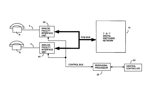
FIG. 1 is a simplified block diagram of a T-S-T
central office switching system where the enhanced SLIC
in accordance with the present invention is used to
advantage.
204268%
'~ FIG. 2 is a block diagram of a line card including
the enhanced SLIC in accordance with the present
invention.
FIG. 3 is a block diagram of one of the two over-
current sense circuits residing in the line controlinterface of the e~hAnc~ SLIC in accordance with the
present invention.
FIG. 4 is a block diagram of the over-current
detector circuit in accordance with the present
invention.
DESCRIPTION OF A PREFERRED EMBODIMENT
Turning now to FIG. 1 of the included drawings
a central office switching system or central office ex-
change of the type to which the invention is used to ad-
vantage is illustrated. The central office switchingsystem includes a time division multiplexed Time-Space-
Time (T-S-T) digital switching network 10 consisting
minimally of an originating time switch and control unit,
a space switch unit and a terminating time and control
unit (not shown). The T-S-T network 10, connects to
Analog Facility Interface Units (AFIU) 30 and 40 via a
(Pulse Code Modulation) PCM BUS. Each AFIU 30 and 40
allows, in this embodiment, the connection of subscriber
lines 3 and 4 respectively to the network 10. Subscriber
lines 3 and 4 further connect to subscriber telephone in-
struments A and B, respectively. The network 10 and each
AFIU 30 and 40 is further connected to a Peripheral Pro-
cessor (PP) 20, via a CONTROL BUS. The PP 20 maintains
control of its environment by scAnn;ng the AFIUs 30 and
40 and controlling the associated network time and con-
trol units. The total control of the network connections
within the network 10 is the responsibility of the Cen-
tral Controller (CC) 50. That is, the central controller
50, via the PP 20, informs the time and control units of
the time switch connections and also informs the space
switch unit of the space switch connections. In addition
the CC 50 maintains a data base of the call processing
20426~32
- and administrative software for the central office
SWit~ i ng system.
Analog voice signals from the transmitter of sub-
scriber instrument A are transmitted to AFIU 30 where
they are converted to PCM encoded digital signals. The
PCM encoded digital signals are then inserted into avail-
able channels on the PCM BUS and transmitted to the digi-
tal switching network 10. Under control of the PP 20 the
PCM enGoAPA digital signals from subscriber A are
switched through the digital switching network 10 and
transmitted to AFIU 40 on the PCM BUS. The received PCM
encoded digital signals are converted back to analog
voice signals and transmitted via subscriber line 4 to
the receiver of subscriber instrument B. The SLIC of the
present invention is located within the AFIU.
Turning now to FIG. 2 of the included drawings a
block diagram of a line card including the enhanced SLIC
is shown. The line card shown in FIG. 2 includes eight
SLICs. Each SLIC is arranged to interface a single sub-
scriber line comprised of a Tip (T) lead and Ring (R)lead to the T-S-T digital switching network 10. The line
card includes four thick-film transmission hybrid (XBRID)
modules 100. All critical analog components of the SLIC
are contained on the XBRID module 100. Each XBRID module
100 further includes two High Voltage Line Interface
(HVLI) circuits such as HVLI lDl and two Hybrid Combo
(HCOMBO) circuits such as HCOMBO 102 along with matched
resistor networks and battery feed transistors (not
shown). An HVLI 101 and a HCOMBO 102 form one functional
SLIC that in combination provide most of the so-called
BORSCHT-functions. In particular, the function of the
r-riber power supply (Battery), line status monitoring
(Signals, Supervision), analog-digital conversion
(Coding) and filter functions and two wire-four wire
transition (Hybrid) are provide by the HVLI 101 and
HCOMBO 102 of each XBRID module 100.
In addition to powering the subscriber line, the
HVLI 101 performs the essential two wire-four wire hybrid
function of splitting the balanced signal on the T and R
20 42682 -
leads to separate transmit/receive paths. The differen-
tial audio signals are transmitted and received to/from
the HCOMBO 102. The HVLI 101 further performs loop su-
pervision, ring trip detection, ground sensing and over-
current detection. A more detailed explanation of theelectrical structure and operation of HVLI 101 may be had
by reference to co-pending Canadian Patent Application
Serial No. 2,042,683-7.
The HCOMBO 102 synthesizes the input impedance of
the SLIC and performs hybrid balance echo cancellation.
Additionally, the HCOMBO 102 converts the differential
audio signals from the HVLI 101 to PCM encoded digital
signals and from PCM encoded digital signals to differen-
tial audio signals. A more detailed explanation of the
electrical structure and operation of HCOMBO 102 may be
had by reference to co-pending Canadian Patent Applica-
tion Serial No. 2,042,680-2.
The remainder of the BORSCHT functions are provided
by the Line Configuration and Protection (LCP) circuit
103, located off the XBRID module 100. The LCP 103 ap-
pears between the T and R leads of a subscriber line and
the HVLI 101. The LCP 103 functions to provide overvolt-
age protection (Overvoltage), the application of ringing
current to the subscriber line (Ringing) and testing of
the subscriber line as well as the SLIC (Test). The LCP
103 contains ring relays which under software control in-
ject ringing current from a ringing generator (not shown)
to the subscriber line. Similarly the subscriber line as
well as the SLIC can be isolated and tested via a test
relay (not shown) that provides facility test (Out Test)
and circuit test (In Test). The test relay allows the
application of test signals from a test program which
resides in the CC 50. The LCP 103 further includes a cut
relay (not shown) which isolates the SLIC from the sub-
scriber line when an over-current condition is detected.
In a digital common logic area of the line card
resides a plurality of Line Control Interface (LCI) cir-
cuits 104. Each LCI 104 performs aIl of the control and
sense logic functions for the two SLICs of an associated
2042682
~ XBRID module 100. In particular, each LCI 104 functions
to administer and control the ringing and test relays,
hook status reporting, dial pulse detection, ring trip,
y-O~Id sensing, and over-current detection. Each LCI 104
connects its associated XBRID module 100 to PP 20 via a
control and sense bus.
Digital logic buffers 105 transmit data from the
HCOMBO 101 of XBRID module 100, to the PCM bus of the
network, and conversely, receive PCM data from the net-
work PCM bus to a respective HCOMBO 102. CODEC Control
circuit 106 is an octal Time Slot Assigner Circuit (TSAC)
device that functions to generate transmit and receive
frame sync pulses to its connected HCOMBO devices 102.
One TSAC 106 connects to all eight HCOMBOs of the line
card. The network provides a required 1.544 MHz clock
with a nominal 50% duty cycle for the purpose of shifting
PCM data in and out of the HCOMBO 102 data registers. A
frame (125~sec) provides for 24 eight bit PCM channels
with one framing bit for synchronization. One such TSAC
device is the TP3155 Time Slot Assigner Circuit manufac-
tured by the National Semiconductor Corporation.
As can be seen in FIG. 2, the four XBRID modules 100
on the line card, include eight SLIC circuits that via
each SLICs associated LCP 103 connect to eight subscriber
lines. Further, each of the four LCI 104 circuits is
co~ected via a control and sense bus to an associated
XBRID module 100 and the HVLI 101 and HCOMBO 102 pair.
Still further, a single CODEC controller 106 connects to
all eight HCOMBO devices 102 via a PCM and CODEC data
bus, allowing the CODEC collL~oller 106 to control the PCM
time slot allocation for each of the eight SLICs.
Finally, the PCM data and control and sense data is
transmitted to the digital switching network 10 via the
TTL buffers 105 and the network bus.
The LCI circuit 104 provides an over-current sense
point to indicate to software when an excessive voltage
AprDArS on the subscriber line. There are two stages of
over-current sense implementation which LCI 104 will sup-
port. First, the over-current would be read by software
_g_
204268~
~- but the CUT relay would not be implemented in hardware.
In the C~con~, the cut relay would be activated. An
over-current condition is ~?~e~ by HVLI 101 and communi-
cated to LCI 104 by developing an active low signal
OVERSENSE.
Turning now to FIG. 3, of the included drawings, one
copy of the two over-current circuits found within LCI
104 is shown. LCI 104 is essentially memory mapped hard-
ware for the time switch of the T-S-T digital switching
network 10. It receives asynchronous peripheral proces-
sor accesses under software control. Control and sense
information is r~ to and from the LCI 104 on a two
bit (one bit per line circuit) parallel bidirectional
bus. The data lead which conveys control and sense data
to the over-current circuit of the present invention is
shown in Fig. 3 as C/S.
The over-current circuit includes an address decoder
200 and a multiplexer 250, that are connected to a four
bit address bus. The type of access information, that
i~, data that collLLols the LCI 104 and sense data that
the peripheral proce~sor reads from the LCI 104, is de-
termined by the four bit address and the card enable
signal CEN. For example, an address of 0011 would ad-
dress the multiplexer 250 to allow the peripheral proces-
sor to read or sense if an over-current condition exists.
An address of 1011 with signal CEN enabled would enable
address decoder 200 and prepare cut register 220 for the
input of data from the C/S data lead. Since the C/S data
lead is bidirectional, signal RPL applied to transceivers
230 and 240 controls the direction of the information
traveling on the C/S data lead. Thereby, allowing the
reading of signal OVRCRNT from the multiplexer 250 (sense
data) or the input of a control data bit (control data)
to the cut register 220. The over-current circuit fur-
ther includes an over-current detector circuit 210 con-
nected to HVLI 101. Signal OVERSENSE is developed in
HVLI 101 when an over-current condition is sensed on the
subscriber loop. OVERSENSE is then coupled into detector
210 where it is tested to ascertain if the over-current
--10--
Z04268~
~ condition is valid. The circuit tests for both dc and ac
over-current conditions and if a valid condition exists,
produces signal OVRCRNT. Signal OVRCRNT is coupled to
multiplexer 250 for transmission to the peripheral
proceCcor.
Simultaneously, signal OVRCRNT is also coupled into
cut register 220. Signal OVRCRNT clears cut register
220, deactivating a cut relay (not shown) which is ar-
ranged to break the tip and ring leads of the subscriber
loop. This immediately removes the over-current condi-
tion and prevents damage to HVLI 101. Once the over-
current sense point is set, it will remain set until
software writes a control bit to the cut register 220,
reactivating the cut relay.
Turning now to Fig. 4 of the included drawings the
over-current detector circuit of the present invention
will be explained. The over-current detector 210 is con-
nected to HVLI 101 via the OVERSENSE signal lead. OVER-
SENSE is connected to a dc on counter 501, a hit counter
502 and a hit timer 503. Counters 501, 502 and timer 503
are used to determine the validity of the OVERSENSE sig-
nal received from HVLI 101. The dc on counter 501 and
the hit counter 502 are connected to over-current regis-
ter 505 where valid over-current signals are latched.
Once set, circuit 505 pro~llc~s o~L~L signal OVRCRNT.
Signal OVRCRNT is then transmitted to multiplexer 250 and
cut clear pulse generator 507. Cut clear pulse generator
507 produces a C~TCLR pulse when a valid over-current
condition is se~e~. This clear pulse is applied to cut
register 220. Clear pulse generator 506 is arranged to
clear over-current register 505 when cut register 220 is
set by software.
With renewed reference to FIG. 4 an explanation of
the manner in which the present invention operates will
now be given. The circuit of the present invention can
detect both dc and ac over-current conditions. For a dc
over-current, dc on counter 501 is held clear as long as
there is no over-current indicated from HVLI 101. A low
logic input on OVERSENSE removes the clear and enables dc
--11--
204268~
-- on counter 501 to begin counting. Counter 501 is clocked
with a 250 Hz clock signal from the CLK input. If OVER-
SENSE remains low for 15 counts (56 milliseconds), then
the over-current register 505 is set, producing signal
G~K~NT. Additionally, OVRCRNT is applied to cut clear
pulse generator 507 where a pulse CUTCLR is generated and
transmitted to cut clear register 220. The CUTCLR pulse
clears register 220 and opens the subscriber loop via a
cut relay (not shown). Once the over-current register
505 is set it will remain set until software writes a
positive logic data bit into cut register 220. The tran-
sition of signal CUTRLY from a low logic level to a high
logic level signal causes the clear pulse generator 506
to produce a clear pulse to the over-current register
505, thereby, clearing register 505.
The detection of an ac over-current condition works
in a similar fashion. A low logic signal at OVERSENSE
enables the hit timer 503 to begin counting. A high to
low transition of the OVERSENSE input also causes the hit
counter 502 to register one hit. Each subsequent low
pulse on OVERSENSE will cause the hit counter 502 to ad-
vance. If three hits are registered before the hit timer
503 reaches a count of 15 (56 milliseconds minimum), then
it is considered a valid ac over-current and the over-
current register 505 is set. However, if the hit timer503 reaches a count of 15 before the hit counter 502
reaches a count of three, then the hit counter and hit
timer are reset by the reset circuit 504 and the next
pulse on OVER~ will restart the ac detection se-
quence. The interaction between the over-current regis-
ter 505 and the cut register 220 remains the same whether
it is a dc or an ac over-current condition.
As can be appreciated from the above description the
over-current detector circuit of the present invention
effectively discriminates between a legitimate prolonged
over-current condition, and a fast erroneous voltage
pulse that may be induced on the loop. Large voltages
directly applied or induced into a subscriber loop can
cause catastrophic damage to the sensitive circuits of
-12-
204Z68~
the SLIC. The over-current detector circuit monitors the
~criber line and is ~i~pose~ to isolate the HVLI 101
from the subscriber loop when a over-current condition is
detected.
Furthermore, it will be obvious to those skilled in
the art that numerous modifications to the present inven-
tion can be made without departing from the scope of the
invention as defined by the appended claims. In this
context, it should be recognized that the essence of the
present invention resides in a new and effective over-
current detector circuit for an enhanced subscriber line
interface.
-13-