Note: Descriptions are shown in the official language in which they were submitted.
~ 9//D~/ ~ ~ ~0
~ 2~4313~
SPECIFICATION
TITLE OF THE INVENTION
Digital Signal Encoding Apparatus
BACKGROUND OF THE INVENTION
Field o~ the Invention
This invention relates to an apparatus ~or encoding an input
digital signal.
DescriPtion of the Prior Art
For high e~iciency encoding o~ audio or voice signals,
there is known an encoding technique by adaptive bit allocation
in which the input signals, such as audio or voice signals, are
divided on the time axis or on the ~requency axis into a
plurality o~ channels and the numbers o~ the bits are adaptively
allocated ~or the respective channels. Among the encoding
techniques of the audio signals by adaptive bit allocation, there
are a sub-band coding (SBC), in which the audio signals on the
time axis are divided into a plurality o~ ~requency bands ~or
encoding, an adaptive trans~orm coding (ATC) in which signals on
the time axis are converted into those on the ~requency axis by
orthogonal transform and divided into a plurality of ~requency
bands in each o~ which adaptive signal encoding is per~ormed, and
a so-called adaptive bit coding (APC-AB), in which the sub-band
encoding and adaptive trans$orm encoding are combined such that
the signals on the time axis are divided into ~requency bands and
the signals of the reæpective bands are converted into baseband
~ 2043133
signals and predictively encoded by nth order linear predictive
analyses, where n is an integer equal to two or more.
In the field o~ high e~iciency encoding, techniques o~ high
e~iciency encoding, in which so-called masking characteristics
of the human auditory sense is taken into account, have been
adopted extensively. The masking e~iect means a phenomenon in
which a signal is masked by another signal and thereby becomes
inaudible. This masking ef~ect is classi~ied into that on the
audio signals on the time axis and that on the signals on the
~requency axis.
The masking e~fect on the audio signals on the frequency
axis is explained. In the case o~ a sine wave Ws having a
~requency ~s' the masking spectrum or masking curve MS,
representing the masking e~ect by the human auditory sense, is
as shown in Fig. 1. By this masking spectrum MS, an area
indicated by hatched lines is masked. Thus the noise within the
masking spectrum MS, i~ any, becomes inaudible, so that, with the
actual audio signal, any noise within the masking spectrum MS is
allowable. Thus the allowable noise level in the case o~ the
sine wave Ws is below the level shown at j in Fig. 9. Also the
masking effect is maximum at the ~requency fs ~ the sine wave Ws
and becomes the lower the more the frequency is removed from the
frequency ~s ~ the sine wave Ws. ~ -
The masking on the audio signals on the time axis isclassified into temporal masking and concurrent masking.
,:
. 2043133
Concurrent masking means such effect in which a smaller sound (or
noise) generated simultaneously with a larger sound is masked by
the larger sound and becomes inaudible. Temporal masking means
an e~ect in which, as shown in Fig. 2, the smaller sound or
noise temporally be~ore and after a larger sound (a high level
signal part C in the ~igure) is masked by the larger sound and
becomes inaudible. With temporal mas~ing, masking o~ the sound
temporally a~ter the larger sound is`~termed ~orward masking and
masking o~ the sound temporally be~ore the larger sound is termed
backward masking. In temporal masking, the ef~ect of ~orward
masking FM in Fig. 2 persists ~or a long time (of the order of
100 msec, ~or example), while that of backward masking BM has a
shorter duration (o~ the order o~ 5 msec, ~or example), on
account o~ the characteristics o~ the human auditory sense. The
masking level or masking quantity is o~ the order of 20 dB and
dB with ~orward masking and with backward masking,
respectively.
Meanwhile, with the above described high e~iciency
encoding, it is desired to achieve ~urther increase in the bit
compression rate L or the amount o~ bit reduction. However, with
the high ef~iciency encoding, in which bit compression is
achieved by taking advantage of the above described masking
e~fect, only one o~ the masking effect on the signals on the
~requency axis or the masking ef~ect on those on the time axis
is taken into account, that is, it has not been tried to take
2~133
both masking e~ects into account simultaneously.
OBJECTS AND SUMMARY OF THE INVENTION
It is there~ore an object of the present invention to
provide a digital signal encoding apparatus in which both the
masking e~ect o~ the signals on the frequency axis and the
masking effect o~ the signals on the time axis are utilized
e~fectively to achieve a further increase in the amount o~ bit
reduction or to lower the bit rate. `
It is another object o~ the present invention to provide a
digital signal encoding apparatus in which deterioration in the
sound quality may be minimized despite the low bit rate.
For accomplishing the above objects, the present invention
provides a digital signal encoding apparatus ~or encoding an
input digital signal comprising dividing means to which said
input digital signal is supplied, said dividing means being
adapted ~or dividing the frequency range of said input digital
signal into a plurality of ~requency bands, first noise level
setting means ~or setting a ~irst allowable noise level of each
frequency band based on the energy o~ each frequency band, second
noise level setting means ~or setting a second allowable noise
level o~ each ~requency band based on the energies of the signals
temporally adjacent to the signals o~ the frequency band under
consideration ~or quantization, ~synthesizing means for
synthesizing said ~irst and second allowable noise levels and
means for quantizing signal components o~ each frequency band
20~3133
with the number o~ bits corresponding to the level o~ the
di~erence between the energy of each ~requency band and the
output o~ said synthesizing means.
According to the present invention, an allowable noise level
which takes into account the masking on the ~requency axis is set
by first noise level setting means ~or the signal o~ the
frequency band under consideration ~or quantization, while
another allowable noise level which takes into account the
masking on the signals temporally adjacent to the signals o~ the
~requency band under consideration is set by second noise level
setting means ~or the same signal o~ the frequency band under
consideration for quantization.
With the digital signal encoding apparatus of the present
invention, the ~requency range o~ the input digital signal is
divided into a plurality o~ ~requency bands so that the bandwidth
is broader towards the side o~ the ~requency bands o~ higher
~requencies. The ~irst allowable noise level is set ~rom one
~requency band to another on the basis of the energy o~ each
frequency band, while the second allowable noise level is set on
the basis o~ the energies o~ the signals temporally adjacent to
the signals o~ the band which is under consideration for
quantization. The signal components o~ each ~requency band are
quantized with the number of bits corresponding to the level of
the di~erence between the sum output of the ~irst and second
allowable noise levels and the energy of each frequency band.
,,
. ~ '
,
2043133
In this manner, both the masking e~ect ~or the signals o~ the
~requency band under consideration on the ~requency axis and the
masking e~ect ~or the signals on the time axis may be utilized
e~fectively ~or increasing the degree o~ bit reduction or
lowering the bit rate while minimizing deterioration o~ the sound
quaIity even though the number o~ bits is reduced.
BRIEF DESCRIPTION OF THE DRAWINGS
Fig. 1 is a chart showing the spectrum of audio signals.
Fig. 2 is a chart ~or illustrating the temporal masking.
Fig. 3 is a block circuit diagram showing the construction
of a digital signal encoding apparatus according to an embodiment
o~ the present invention.
Fig. 4 is a chart ~or illustrating the critical bands.
Fig. 5 is a chart ~or illustrating the Burke spectrum.
Fig. 6 is a circuit diagram showing a ~ilter circuit.
Fig. 7 is a chart for illustrating a masking spectrum.
Fig. 8 is a chart ~or illustrating the synthesis of a
minimum audibility curve and the masking spectrum.
Fig. 9 is a block circuit diagram showing the construction
o~ a modified embodiment.
Fig. 10 is a chart for illustrating the resolution o~ the
~requency domain and the time domain.
DESCRIPTION OF THE PREFERRED EMBODIMENTS
By re~erring to the accompanying drawings, certain
illustrative embodiments of the present invention will be
20~3133
explained in detail.
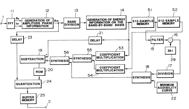
Referring to Fig. 3, a digital signal encoding apparatus
according to the present invention includes a band-dividing
circuit 13, a sum detection circuit 14, a filter 15, a
subtraction circuit 16, a division circuit 17 and a synthesizing
circuit 18, operating conjointly as first noise level setting
means for dividing the input digital signals into a plurality of
~requency bands so that the bandwidth`will be broader towards the
side o~ the ~requency bands o~ higher ~requencies, and for
setting a first allowable noise level on the band-by-band basis
based on the energy o~ each band. The digital signal encoding
apparatus also includes memories 51 and 52, coe~icient
multiplication units 53 and 54 and a synthesizing circuit 55,
operating conjointly as second noise level setting means for
setting a second allowable noise level based on the energies of
signals temporally adjacent to the signals of a ~requency under
consideration ~or quantization. The signal encoding apparatus
~urther includes a synthesizing circuit 56 as synthesizing means
~or synthesizing the allowable output noise levels o~ the ~irst
and second-noise level setting means, and a quantization circuit
24 ~or quantizing signal components of each ~requency band with
the number o~ bits corresponding to the level o~ the difference
between the energy o~ each ~requency band and the output ~rom the
synthesizing circuit 56. Thus, with the present apparatus, the
~irst allowable noise level which takes the masking on the
2~3133
~requency axis and a minimum audibility curve into account is set
by the first noise level setting means ~or the signal o~ the
frequency band under consideration ~or quantization, while the
second allowable noise level which takes the temporal masking by
signals temporally adjacent to the signals of the frequency band
under consideration into account is set by the second noise level
setting means for the same signal o~ the frequency band under
consideration. The quantization ou~put from the quantization
circuit 24 is outputted via a buf~er memory 25 at an output
terminal 2 o~ the present digital signal encoding apparatus.
It is noted that, in the present apparatus, shown in Fig.
3, an adaptive trans~orm encoding (ATC) is employed, in which
audio signals, for example, are processed by FFT (fast Fourrier
trans~orm) ~or converting the signals on the time axis into those
on the ~requency axis, and the resulting signals on the frequency
axis are encoded, or re-quantized. More speci~ically, referring
to Fig. 3, the audio signals, which are the signals on the time
axis, are supplied to an input terminal l and thence transmitted
to a FFT circuit 11. In the FFT circuit 11, the audio signals
on the time axis are converted at a predetermined time interval,
~or example, at every ~12 samples, into signals on the ~requency
axis, ~or producing FFT coef~icients each consisting of a real
number component Re and an imaginary number component Im. These
FFT coe~ficients are transmitted to an amplitude phase
information generating circuit 12, where an amplitude value Am
2~3~33
.
and a phase value are produced from the real number component Re
and the imaginary number component Im, with the in~ormation o~
the amplitude value Am being entered to the present apparatus as
the input digital signal. It is noted that the human auditory
sense in general is sensitive to the amplitude on power in the
frequency domain, even though it is rather dull to the phase.
With this in view, only the amplitude value Am is taken out ~rom
the output o~ the amplitude phase information generating circuit
12 as the above mentioned input digital signal.
The input digital signal o~ the amplitude value Am thus
produced is transmitted to the band-dividing circuit 13, where
the input digital signal, expressed as the amplitude value Am,
is divided into, ~or example, so-called critical bands. The
critical bands take human auditory characteristics or ~requency-
analyzing capability into account. Thus the frequency range of
O to 24 k~z is divided into 24 ~requency bands so that the
bandwidths o~ the bands will become broader in the direction of
the higher frequency bands. It is noted that the human auditory
sense has characteristics of a sort o~ bandpass ~ilters, with the
bands o~ the ~requency range divided by the filters being termed
the critical bands shown in Fig. 4. In this ~igure, the number
o~ the critical bands is 12 and the bands are termed B1 to B12.
The amplitude values Am ~or the-critical bands, such as 24
critical bands, obtained at the band-dividing circuit 13, are
transmitted to the sum detection circuit 14, where the energies
2~l~3133
or spectral intensities o+` each band are +`ound by taking the sum
of the amplitude values in each band (the peak value or the mean
value of the amplitude values Am or the energy sum in each band).
The outputs o~ the sum detection circuit 14, that is the spectrum
of the sums o~ the bands, are generally termed the Burke
spectrum, the values of which are shown for example in Fig. 5.
For taking the effect of the Burke spectrum on the masking
into account, a predetermined weighting function is convolved on
the burke spectrum (convolution). To this effect, the outputs
of the sum detection circuit 14, that is the values of the burke
spectrum SB, are transmitted to a filter circuit 15 by means of
a memory 51, which reads and/or writes the outputs of the sum
detection circuit 14 each consisting of, for example, 512
samples. The ~ilter circuit 15 is constituted by delay (z1)
elements lOlm2 to lOlm+3 for sequentially delaying the input data,
multiplication units 102m3 to 102m+3 for multiplying the outputs
from the delay elements by filter coefficients (weighting
+.`unctions), and a summation circuit 104. More specifically, the
outputs of the delay elements are multiplied at the
multiplication units 102m_3, to 102~+3 by, for example, filter
coefficients 0.0000086, 0.0019, 0.15, 1, 0.4, 0.06 and 0.007,
respectively, by way of performing a convolution of the Burke
spectrum SB. By this convolution, the sum oY the effects from
the adjacent values of the Burke spectrum on the values of the
Burke spectrum under consideration, as shown by broken lines in
2~3~33
Fig. 5, is found as the outputs ~rom the summation circuit 104,
and the results of convolution is outputted at output terminal
105.
Meanwhile, i~ a level a, corresponding to the first
allowabIe noise level used ~or calculating the masking spectrum
(allowable noise spectrum) of the Burke spectrum SB, is low, the
masking spectrum or masking curve with respect to signals on the
~requency axis is also low, so thà~ it becomes necessary to
increase the number o~ bits allocated for quantization by
quantization circuit 24. Conversely, i~ the level a is higher,
the masking spectrum is increased, so that it becomes possible
to reduce the number of bits allocated ~or quantization. It is
noted that the level a is a noise level which will prove to be
the above mentioned ~irst allowable noise level ~or each critical
band upon deconvolution which will be explained subsequently.
In general, the spectral intensities or energies o~ the audio
signals are low in the higher ~requency range. With this in
mind, the level a is set so as to be higher towards the higher
~requency range having the low energy values, ~or reducing the
number o~ bits allocated ~or the higher ~requency range. Thus,
in the first noise level setting means, the level a set so as to
be higher ~or the same energy value for the critical bands of
higher ~requencies.
Thus the present apparatus calculates the level a
corresponding to the first allowable noise level and controls the
2~133
level a so as to be higher towards the side o~ the bands o~
higher $requencies. To this end, the output o~ the filter
circuit 15 is supplied to the subtracter 16 adapted ~or finding
the level a in the convolved region. The subtracter 16 is
supplied with a permission ~unction (a ~unction expressing the
masking level) ~or ~inding the level a. The level a is
controlled by increasing or decreasing the permission function,
which is supplied ~rom a ~unction generating circuit 29.
The level a corresponding to the allowable noise level may
be ~ound ~rom $ormula (1)
a = S - (n - ai) (1)
where i is the number given to the critical bands in the order
o~ increasing frequencies.
In this ~ormula (1), n and a are constants, with a>O, S is
the intensity o~ the Burke spectrum following convolution and (n-
ai) in ~ormula (1) becomes the permission ~unction. Since it is
more advantageous to decrease the number o~ bits irom the higher
range with lesser energy amounts ~or the sake o~ decreasing the
number o~ bits on the whole, as discussed above, the values n and
a are set so that n=38 and a=l in the present embodiment, whereby
satis~actory encoding can be achieved without deterioration in
the sound quality.
The level ~ found in this manner is transmitted to the
division unit 17. The division unit 17 ~unctions to deconvolve
the level a in the convolved region. Thus, by this
12
2043133
deconvolution, the masking spectrum can be obtained ~rom the
level a. That is, this masking spectrum proves to be the
allowable noise spectrum ~ound ~rom one band to another.
Although deconvolution necessitates a complex processing
operation, it is per~ormed with the present embodiment with the
use of the simplified division unit~lq.
The masking spectrum is transmitted to a subtracter 19 by
means of synthesizing circuits 1~ and`56. To the subtracter 19,
the output of the sum detection circuit 14, that is the Burke
spectrum SB, is supplied by means o$ a delay circuit 21. Thus
the masking spectrum and the burke spectrum SB are processed by
the subtracter 19 by a subtracting operation, whereby, as shown
in Fig. 7, the Burke spectrum SB is masked at lower than the
level indicated by the level of the masking spectrum MS.
The output of the subtracter 19 is supplied to the
quantization circuit 24 by means of a ROM 20. In the
quantization circuit 24, the amplitude Am supplied thereto by
means of the delay circuit 23 is quantized with the number of
bits conforming to the output from the subtracter 19. In other
words, the signal components o~ each ~requency band are quantized
with the number of bits allocated in accordance with the level
difference between the energy of each critical band and the
output of the synthesizing circuit ~6. Meanwhile, the delay
circuit 21 is provided for delaying the Burke spectrum SB from
the sum detection circuit 14 in consideration of the delay in
13
2~3~33
each circuit upstream o~ the synthesizing circuit ~6, while the
delay circuit 23 is provided for delaying the amplitude Am in
consideration of the delay caused in each circuit upstream o~ the
ROM 20. The ROM 20 stores the data o~ the number of bits
allocated for quantization in the quantization circuit 24 and
outputs the data of the allocated number o~ bits con~orming to
the output of the subtracter 19.
It will be noted that, in the sy`nthesis by the synthesizing
circuit 18, the data indicating the so-called minimum audibility
curve (equal loudness curve) RC, which represents the
characteristics o~ the human auditory sense, ~rom a minimum
audibility curve generating circuit 22, shown in Fig. 8 and the
masking spectrum MS, are synthesized. By synthesizing the
minimum audibility curve RC and the masking spectrum MS in this
manner, the allowable noise level may be de~ined as the upper
boundary of an area indicated by the hatched lines in the
drawing, so that the number o~ bits allocated to this area may
be diminished. Meanwhile, in Fig. 8, the ~requency range has
been divided into the critical bands shown in Fig. 4 and the
signal spectrum SS is shown simultaneously.
With the present digital signal encoding apparatus, the
allowable noise level is increased and the allocated number of
bits decreased towards the higher ~requency side with the lesser
amount o~ the energy, while the signal components are quantized
with the number of bits which takes into account the masking of
14
20~31~3
the signals on the $requency axis ~rom one band to another, so
that the amount of bit reduction may be increased, that is, the
bit rate may be decreased.
Also, in the present embodiment, the allocated number of
bits ~or quantization is determined in consideration o~ the above
mentioned masking on the frequency axis, while the second
allowable noise level o~ the band under consideration is set on
the basis o~ the energies o~ the signals temporally adjacent to
the band under consideration ~or quantization. In this manner,
the allocated number o~ bits for quantization which takes into
account the temporal masking on the time axis may be determined
simultaneously. That is, the second allowable noise level is
additionally set for the ~requency band under consideration at
the current time point, for which the first allowable noise level
has been set in the ~irst noise level setting means, so that the
temporal masking by signals lying at the temporally adjacent
earlier and later points on the time axis may also be taken into
account. To this e~ect, not only the output o~ the synthesizing
circuit 18 but also the output o~ the synthesizing circuit 55 o~
the second noise level setting means is supplied to the
synthesizing circuit 56.
In this manner, the level o~ temporal masking based on the
energies o~ the signals lying at the~adjacent time points with
respect to the signal at the current time point o~ the band under
consideration is computed as the signal of the second allowable
2~431~3
noise level and supplied to the synthesizing circuit 55, so that
the allowable noise level by these temporally adjacent signals
is ~ormed by the synthesizing circuit 55.
For obtaining the second allowable noise level, the present
apparatus is provided with the memory 51 adapted +or
writing/reading the output o+~ the sum detection circuit 14 ~or
every 512 samples, memory 52 similar to memory 51, coef$icient
multiplication 53, 54 and the synthesizing circuit 55. That is,
i$ the time point at which the output o+~ memory 51 is obtained
is the current ti~e point To~ the time point at which the output
o$ the sum detection circuit 14 is supplied to the memory 51 is
the later time point T+1 which is temporally a$ter the current
time point To ($uture time relative to current time point To)~
while the time point o$ outputting +'rom the memory 52 is the
earlier time point T_1 temporally be$ore the current time point
To (past time relative to current time To)~
The signal at the later time point T+1, that is the output
o~ the sum detection circuit 14, is supplied to the coe~$icient
multiplication unit 53. In the coe$$icient multiplication unit
53, the signal at the later time point T+1 is multiplied by a
multiplication coe$$icient which has been determined in
consideration o$ the temporal masking by the signal o$ the band
under consi.deration supplied at the ~ater time point T+1 to the
unit 53 on the signal o$ the band under consideration at the
current time point TO(background masking). That is, the
16
2~3133
multiplication coe~ficient is set in consideration o~ the effects
brought about at the synthesis circuits 55 and 56. I~ the signal
at the later time point T~l is normalized to 1, the signal at the
later time point T+1 is multiplied by a multiplication
coe~ficient kB corresponding to the level at which the backward
masking by the signal at the later time point T+1 acts on the
signal at the current time point To~ The signal at the earlier
time point T_l, that is the output ~rom memory 52, is supplied to
the coe~icient multiplication unit 54. At the coe~ficient
multiplication unit 54, the signal at the earlier time point T1
is multiplied by a multiplication coefficient determined in
consideration o~ the temporal masking effect o~ the signal of the
band under consideration at the current time point To by the
signal o~ the band under consideration supplied at the earlier
time point T_l to the coe$ficient multiplication unit 54 (forward
masking). Thus the multiplication coe~icient is also determined
to take the e~ect brought about at the synthesizing circuits 55
and 56 into account. I~ the signal at the earlier time point T
is normalized, the signal at the earlier time point Tl is
multiplied by a multiplication coe~ficient kp corresponding to
the level at which the forward masking by the signal at the
earlier time point T1 acts on the signal at the current time
point To~ The output o~ the coe~icient multiplication units 53
and 54 are synthesized in the synthesizing circuit 55 into the
above-mentioned second allowable noise level. The synthesizing
17
2~3~ 33
circuit 55 operates for adding the outputs of the coe~icient
multiplication units 53 and 54 to together. The so-produced
output of the synthesizing circuit 55 is supplied to the
synthesizing circuit 56.
In the synthesizing circuit 56, the larger one of the
outputs of the synthesizing circuit 55 or 18 is selected or,
alternatively, the outputs of the circuits 55, 18 are added
together after multiplication by predetermined weighting
coefficients. The latter synthesizing operation by addition may
also be so performed that, in finding the second allowable noise
level, the energies of the overall frequency bands are taken into
account.
The above described minimum audibility curve synthesizing
operation may be omitted in which case the minimum audibility
curve generating circuit 22 and the synthesizing circuit 18 shown
in Fig. 3 may be eliminated. Thus the output of the subtracter
16 may be transmitted directly to the synthesizing circuit 56
a~ter deconvolution by the division circuit 17.
With the above described digital signal encoding apparatus,
the first allowable noise level which takes the masking on the
frequency axis into account is set by the first noise level
setting means for the signals under consideration for
quantization, at the same time that the second allowable noise
level, which takes the temporal masking by signals temporally
adjacent to the signals of the band under consideration into
18
2~3133
account, is also set by the second noise level setting means Ior
the same signals under consideration ~or quantization. The
number of bits allocated for quantization by the quantization
circuit 24 is set from one band to another on the basis of these
$irst and second allowable noise levels, so that the amount of
bit reduction may be increased, or conversely, the bit rate may
be lowered, without degrading the sound quality.
The present invention may also bè applied to a band-dividing
and encoding apparatus, shown for example in Fig. 9, besides the
apparatus for adaptive transIorm and encoding, shown for example
in Fig. 3.
Referring to Fig. 9, audio signals on the time axis are
supplied via input terminal 61 to bandpass ~ilters (BPFs) 621 to
623. The BPFs 621 has the Irequency range o~ O to 6 kHz of the
input audio signals as the passband, the BPF 622 has the
Irequency range o~ 6 to 12 kHz o~ the input audio signals as the
passband and the BPF 623 has the ~requency range o~ 12 to 24 kHz
OI the input audio signals as the passband. The outputs of these
BPFs are transmitted to ~ast Fourrier trans~orm (FFT) circuits
631 to 633. In the FFT circuit 631, FFT processing is performed
Ior example for every 128 samples, whereas, in the FFT circuits
632 and 633, FFT processing is performed for example for every 64
samples. The outputs OI these FFT circuits are transmitted to
quantization circuits 641 to 643, similar to the circuitry
downstream of the FFT circuit 11 in Fig. 3, so as to be processed
19
2~31~j3
similarly to the preceding embodiments. The outputs o~ the
quantization circuits 641 to 643 are synthesized in a
synthesizing circuit 65 and outputted at an output terminal 66.
With the arrangement shown in Fig. 9, it is possible to increase
the amount of bit reduction, while minimizing the deterioration
in the sound quality, similarly to the apparatus shown in Fig.
1.
Fig. 10 shows the resolution in the frequency domain and the
time domain in the apparatus shown in Fig. 10, wherein a unit o~
processing by band division or fast Fourrier transform is shown
and each block is designated by two parameters m and n is b(m,
n), where m is the band number and n the time number. It is seen
~rom Fig. 8 that, ~or the lower range o~ 0 to 6 kHz, each block
in each ~requency band has a time duration (time resolution) of
10.67 msec, and that, for the mid and higher ~requency ranges of
6 to 12 kHi~ and 12 to 24 kHz, respectively, each block has the
time duration o~ 5.3 msec and the time duration o~ 2.67 msec,
respectively.
" ~ ~, .. . ........................ .