Note: Descriptions are shown in the official language in which they were submitted.
~9-89-100
2~3~77
TRIPLE FIELD BUFFER FOR TELEVISION IMAGE STORAGE AND
VISUALIZATION ON RASTER GRAPHICS DISPLAY
FIELD OF THE INVENTION:
This invention relates generally to the display of
television images with a non-interlaced display terminal
and, in particular, to a display system including a frame
buffer and control apparatus therefor for providing
access to digitized television color image data for
accomplishing digital filtering, motion detection and
correction and for accomplishing synchronization.
BACKGROUND OF THE INVENTION:
A desirable feature in certain graphics systems, such as
a multi-media workstation, is the display of an
interlaced image, such as a color television image, with
a non-interlaced graphics display screen. However,
several problems must be overcome in order to provide
this capability in a satisfactory manner.
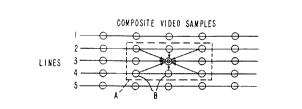
A first problem relates to enhancing the quality of the
television image. One known method for providing image
enhancement involves a digital filtering or decoding
technique, as depicted in Fig. la. However, this
technique requires real-time access, relative to the
incoming video, to a neighborhood (A) of pixels (B) that
are located on three consecutive television lines of a
video field.
A second problem is related to accomplishing
motion-adaptive deinterlacing. As il]ustrated in Fig. lb
this technique requires an access to pixels (B) located
on three television lines. Two of the three line belong
to a current video field while the third line, shown as a
dashed line, is associated with a previous video field.
Additionally, all three of the lines must be synchronized
with the image lines of the graphics display.
'09-89-100 2
~ ~ ~ 3 ~ ~7
A third problem is related to achieving a full
synchronization of the deinterlaced television image
relative to the graphics image. Such synchronization
implies that fully stored frames, each frame comprising
two fields, of television video must be used for the
visualization of the television image on the graphics
screen.
Aspects of the second and third problems are further
illustrated in Figs. lc and ld. Fig. lc shows a position
of an object, represented by a vertical line, in two
consecutive television fields when the object is moving
in a horizontal direction. The first field is depicted in
Fig. lc(a) while the second, consecutive field is
depicted in Fig. lc(b). It can be seen that due to the
horizontal offset between the object image in the two
fields that if all lines of both television fields are
displayed simultaneously on a graphics screen, as
depicted in Fig. lc(c), the image of the object is
blurred.
Fig. ld illustrates the case, for the same moving
vertical object, when the graphics screen is not
synchronized with incoming television video. As a
result, if a new field is partially written into a frame
buffer that contains a previous field the image of the
moving object is split. Fig. ld(c) illustrates a
combined effect of deinterlacing and image splitting. As
can be seen the net result is a blurring of the
television image when displayed upon the non-interlaced
graphics display screen.
In U.S. Patent No. 4,694,325, issued September 15~ 1987,
S. Mehrgardt discloses an interface circuit for
interfacing a color television receiver to a home
computer wherein the home computer has a graphics clock
signal unsynchronized with that of the television
receiver. The circuitry of Mehrgardt includes a digital
delay line having cascaded delay stages. However
Mehrgardt is concerned only with already decoded Red,
~09-89-100 3 2 Q ~ 3 ~
Green and Blue signals and not with the reception and
subsequent display of a composite signal.
In U.S. Patent No. 4,344,075, issued August 10, 1982, J.
Rudy discloses a system for eliminating ragged vertical
edges displayed by a NTSC color carrier on a
non-interlaced display. Rudy discloses timing control
circuitry that is operative only during a selected single
scan line of a non-display portion of each successive
field of a given non-interlaced television raster
scan-line pattern (col. 2, lines 45-61).
In U.S. Patent 4,698,674, issued October 6, 1987, L.
Bloom discloses a data converter for converting
sequentially digitized interlaced data, from a television
camera or other data source, to non-interlaced data for
storage in a computer memory. The approach of Bloom is
to store two fields of the image in a memory. Bloom
apparently assumes that the fields of the television
image are synchronized (gen-locked) with the frames of
the graphics screen. However, .in practically all
applications this is not the case. Instead, the timing of
a non-interlaced graphics controller is typically totally
independent from a television video source.
Other references of general interest include the
following. In U.S. Patent No. 3,970,776, July 20, 1976 K.
Kinuhata et al. disclose a system for converting the
number of lines of a television signal having interlaced
frames, each frame formed by two adjacent interlaced
fields. In U.S. Patent No. 4,484,188, issued November
20, 1984 G. Ott discloses video signal generation
circuitry for improving the resolution of a video signal
by forming additional video scan lines between successive
scan lines. The system of Ott forms the additional video
scan line by combining video attributes of adjacent scan
lines. In U.S. Patent No. 4,480.267~ issued October 30,
1984, P. van den Avoort et al. disclose field
interpolation for obtaining substantially equal
amplitudes of information from each of two successive
~09-89-100 4 2~ ~3~ 77
fields of a television signal. van den Avoort is
concerned with a conversion from a 313-line television
picture to a 625-line television picture. In U.S. Patent
No. 4,694,348, issued September 15, 1987, K. Kamiya et
al. disclose a scan interlace converter for a liquid
crystal display panel of a television receiver. In U.S.
Patent No. 4,660,070, issued April 21, 1987, Nishi et al.
disclose a video display processor for writing video
image data into a video memory. The video display
processor generates memory address data in accordance
with horizontal and vertical synchronization signals. In
U.S. Patent No. 4,518,984, issued May 21, 1985 H.
Mitschke discloses circuitry including a video frame
store 221 for obtaining a flicker-free image when
producing a combined text and graphics (Videotext)
display.
However, none of the forgoing U.S. Patents either
singularly or in combination teach a method or apparatus
that overcomes in a satisfactory manner all of the above
described problems relating to image quality enhancement,
motion-adaptive deinterlacing and synchronization when
displaying an interlaced image, such as a television
signal, with a non-interlaced graphics display system.
It is thus an object of the invention to provide method
and apparatus for displaying an interlaced image signal
on a non-interlaced graphics display screen.
It is a further object of the invention to provide method
and apparatus for dlsplaying on a non-interlaced graphics
display screen a television color image frame comprised
of two interlaced fields; the invention providing three
field buffers, two for storing the two fields of a
completed frame while the third field buffer stores a
current television field.
''09-89-100 5 2~ ~3~77
SUMMARY OF THE INVENTION
The foregoing problems are overcome and the objects of
the invention are realized by a method and apparatus for
displaying, with a non-interlaced display system, an
image signal expressive of an interlaced image. The
interlaced image may be provided by a composite color
television signal that provides a plurality of separately
provided image fields. In accordance with a method of the
invention there are disclosed the steps of (a) storing in
a first memory a first image field; (b) storing in a
second memory a second image field; (c) reading the first
and the second memories; (d) simultaneously displaying on
a display screen the first and the second image fields as
a single image frame; and (e) while performing the step
of reading the method includes a step of storing in a
third memory a third image field. For image fields
numbered 1, 2, 3, 4, 5...n.. the system of the invention
reads the image fields two at a time in accordance with a
predetermined sequence given by: 1 and 2, 2 ~nd 3, 3 and
4, 4 and 5, ... (n - 1) and n, n and (n + 1).
For a case where the image frame is selected to have a
longer duration than an image field the invention detects
a relationship between the image frame and the image
field and alters the predetermined display sequence such
that the image fields are displayed in a sequence given
by: (n - 2) and (n - 1), (n - 1) and n, and (n + 1) and
(n + 2).
For a case where the image frame is selected to have a
shorter duration than an image field the invention alters
the predetermined sequence such that the image fields are
displayed in a sequence given by: (n - 2) and (n - 1), (n
- 2) and (n - 1), and (n + 1) and ~n + 2).
A frame buffer of the invention has a 3x3, a 4x3 or an
8x3 arrangement of memory blocks, each of the blocks
storing a portion of a television field. The frame buffer
~09-89-100 6 2~3~ ~
is read out such that, for example, a 3x3 neighborhood of
pixels are provided in parallel for display or for
subsequent pre-display processing such as interpolation.
BRIEF DESCRIPTION OF THE DRAWING
The above set forth and other features of the invention
are made more apparent in the ensuing Detailed
Description of the Invention when read in conjunction
with the attached Drawing, wherein:
Fig. la illustrates a conventional digital filtering or
decoding scheme that operates on a neighborhood of image
pixels selected from three consecutive scan lines;
Fig. lb illustrates a techni~ue for achieving
motion-adaptive deinterlacing;
Figs. lc and ld illustrate a deinterlacing effect and a
deinterlacing effect with split screen, respectively,
when displaying with a prior art system a linear,
vertically disposed object that is moving in a horizontal
direction;
Fig. 2 shows in block diagram form one embodiment of the
the invention having a television decoder serially
positioned before a frame buffer and an interpolator
positioned after the frame buffer;
Fig. 3 shows in block diagram form another embodiment of
the invention having the television decoder serially
positioned after the frame buffer;
Fig. 4 shows in block diagram form another embodiment of
the invention having the television decoder and the
lnterpolator serially positioned after the frame buffer;
Fig. 5 illustrates a presently preferred 3 by 3 memory
block organization of the frame buffer;
rog-89-100 7
2~31 ~7
Fig. 6 illustrates in greater detail one embodiment of a
frame buffer memory block;
Fig. 7 illustrates in greater detail another embodiment
of a frame buffer memory block;
Fig. 8a illustrates a preferred frame buffer video line
storage se~uence;
Fig. 8b illustrates the storage sequence of Eig. 8a in
greater detail;
Fig. 9 is a timing diagram that illustrates the operation
of the disp'ay system of the invention for a plurality of
consecutively displayed high resolution frames;
Fig. 10 is a timing diagram showing in greater detail a
relationship of an increment (INC) signal in relation to
high resolution and television vertical sync signals;
Fig. 11 is a block diagram that illustrates in greater
detail the serializer block of Figs. 2, 3 and 4;
Fig. 12 is a block diagram that illustrates in greater
detail the frame buffer controller block of Figs. 2, 3
and 4;
Fig. 13 is a block diagram that illustrates in greater
detail the delta timing generator block of Fig. 12;
Fig. 14 is a timing diagram that illustrates the
operation of the delta timing generator block of Fig. 13;
Fig. 15 is a block diagram that illustrates in greater
detail a portion of the television address generator
block of Fig. 12;
Fig. 16 is a block diagram that illustrates in greater
detail another portion of the television address
generator block of Fig. 12;
~09-89-lO0 8 2 ''~
Fig. 17 is a block diagram that illustrates in greater
detail the video refresh address generator block of Fig.
12;
Fig. 18 is a timing diagram that illustrates the
operation of the video refresh address generator block of
Fig. 17;
Fig. l9 is a block diagram that illustrates in greater
detail the scan control block of Figs. 2, 3 and 4;
Fig. 20 is a block diagram that illustrates in greater
detail the organization of the line memories of Fig. 4;
and
Figs. 21, 22 and 23 are tables illustrating, for the
different embodiments of the invention, various aspects
of the operation of reading sequences of lines from the
frame buffer for display.
DETAII.ED DESCRIPTION OF PREFERRED EMBODIMENTS
OF THE INVENTION
Figs. 2, 3 and 4 illustrate in block diagram form three
presently preferred embodiments of the invention. The
embodiment shown in Fig. 2 illustrates a system 10 that
stores component digital video within a frame buffer 12
that is 16 bits in depth. The system 10 also includes an
interpolator and solves two of the previously described
problems, namely motion artifact elimination and full
synchronization of television and graphics images.
Although requiring more memory to store the television
image than do the other embodiments of the invention the
em~odiment of Fig. 2 provides a full solution for s~;stems
using component video representation such as production
HDTV standards (SMPTE 240M standard) or Super-VHS systems
having higher quality than NTSC. It is noted that there
is no need for a television decoder for systems such as
HDTV or Super-VHS that employ chrominance/luminance
analog component inpllts. In this case, a TV decoder is
~09-8g- 100 9
31 77
not needed although an additional Analog-to-Digital
Converter (ADC) is required to digitize luminance and
chrominance components.
Discussing now the embodiment of Fig. 2 in greater detail
an Input Analog Composite Video Signal from a television
signal source .is applied to ADC 14. ADC 14 provides a
Digital Composite Video Signal. An eight bit resolution
ADC l~ output has been found to provide adequate picture
quality. The Digital Composite Video Signal is applied
to a conventional television decoder 16 that provides a
digital luminance (Y) output, a digital chrominance (C)
output, a television vertical sync (T W S) signal, a
television horizontal sync (TVHS) signal, and a
television field indicator signal EVENFIELD.
Suitable devices for providing converter 14 and decoder
16 functions, except EVENFIELD generation, are
manufactured by the Philips Corporation as device part
numbers TDA8708 and SAA9051. These devices are described
in "Digital Video Signal Processing" Philips Components
Manual No. 9398 063 30011. It should be noted that both
12 bit and 16 bit devices are available for use and that
these and other devices are available that correspond to
the CCIR 601-1 recommendation for digital television
encoding and transmission as set forth in "Handbook of
Recommended Standards and Procedures, International
Teleproduction Society", 1987, p.62. The generation of
the EVENFIELD signal is described below.
The luminance and chrominance signals are each expressed
with ei~ht bit resolution and are provided to the frame
buffer 12 for storage. The TVVS, TVHS and EVENFIELD
signals are provided to a frame buffer controller 18
where these signals are employed in a manner which will
be discussed.
Frame buffer controller 18 generates a plurality of
video RAM (VRAM) control signals, including row address
strobes (RAS), a column address strobe (CAS), a
'09-89-100 10
2 ~3 ~ 3 ~
transfer/output enable signal TR/QE, a frame buffer
address (FBAD), and a frame buffer write enable (FBWE).
The controller 18 hardware set-up data is loaded from a
host computer data bus (DB). The frame buffer control
signals are generated and used in a manner described in
the selected VRAM specification. For example, one
suitable type of device is manufactured by Toshiba and is
known as a TC24256 1 Mbit VRAM. Although frame buffer 12
is preferably comprised of VRAM devices the use of VRAMs
is not essential. The same result can be achieved using
conventional dynamic RAM (DRAM) devices but with a
requirement for more memory chips in order to provide the
required memory bandwidth at the output of the frame
buffer 12.
Controller 20 generates a high resolution graphics image
(HR VIDE0) signal. Controller 20 also provides timing
functions for a high resolution color monitor 22, such as
a high resolution vertical sync (HRVS) signal and a high
resolution horizontal sync (HRVS) signal. The HRVS and
HRHS signals are also used as inputs to the frame buf~er
controller 18. The controller 20 generates a serial clock
SCLK for shifting data from the serial port of the VRAMs
and a high resolution video clock HRVCLK for shi~ting
data from a serializer 24. HRVCLK corresponds to the
overall number of pixels on a horizontal line of the high
resolution color monitor 22. SCLK is derived by dividing
HRVCLK by three. The high resolution color monitor 22 has
a pixel resolution of, for example, 1024x1024 displayable
pixels.
With each SCLK, the output of the frame buffer 12
provides to the serializer 24 nine 16 bit pixels for a
total of 144 bits. The nine pixels represent a 3x3 pixel
neighborhood comprised of 144 bits as shown in Fig. la.
In other words, the frame buffer 12 delivers three
sampled television l.ines by three pixels to the
serializer 24 at a serial clock time, although only one
line will be shown finally on the display screen of
monitor 22. The serializer 24 thus converts the parallel
'09-89-100 11 ~ 7
output of the frame buffer 12 to a sequential pixel data
stream to eventually be displayed pixel-by-pixel on the
display screen.
Traditionally, a serializer is employed to serially shift
only one line of data read in parallel from a frame
buffer. However, in accordance with the invention three
lines are read in parallel from the frame buffer 12.
Hence, during each HRVCLK period, the serializer 24
output shifts out three vertically adjacent pixels (48
bits) to the scan control device 26.
As a consequence of a "three by three" block memory
organization described in detail below the three lines at
the output of the serializer 24 are not necessarily
consecutive video lines. Moreover, their order is
variable and depends on the particular addresses of the
frame buffer where the lines are located. The scan
control device 26 rearranges the output of the serializer
24 in a manner described in detail below, providing a
required line order arrangement to the input of the
interpolator 26a.
If motion correction processing is not employed then the
output of the scan control device 26 may be coupled
directly to a color matrix 28. Furthermore, this
si.mplest case does not require access to three television
lines in para]lel. However, the three by three frame
buffer organization is still employed to achieve proper
synchronization between an incoming television image and
the displayed graphics image.
If motion detection and correction is employed, as
illustrated in Fig. 2, then the interpolator 26a is
installed as shown between the scan control 26 and the
color matrix 28. A suitable interpolator architecture
and operational description is found in the literature,
such as in an article "Improved Definition Televlsion" by
Leonard ~eldman, Radioelectronics Magazine, January 1989,
p.43.
09-89-lO0 12 2 ~ ~ 3 ~ ~ 7
It should be noted that the system described by Feldman
cannot be used when two independent video sources are to
be shown on the same screen. The interpolator requires
access to three television lines simultaneously, two of
which belong to a current television field and one of
which belongs to a previous field. The source assumes
that the television line rate is simply doubled on the
output, i.e. the video output is a direct function of the
video input. For this case, the current field is always
present on the inputs of the system, and the previous
field is stored. Using one more line delay, the necessary
three lines become available at the input of the
interpolator. However, as was previously stated a high
resolution image is typically absolutely independent of a
second image source, and the current video field is
asynchronous with the frame buffer output. The present
invention overcomes this problem by always providing the
required data to the input of the interpolator 26a.
As was stated the interpolator 26a provides an input
signal to the color matrix 28. The color matrix 28
converts, in accordance with an applicabie standard such
as CCIR 601, an eight bit luminance signal and an eight
bit chrominance signal to eiqht bit red, eight bit blue
and eight bit green signals. The color primary signals
serve as an input to multiplexer 30. A second input to
the multiplexer 30 is the HR VIDE0 signal comprised of 24
bit pr;mary colors from the controller 20.
Selection of the high resolution television image or the
HR VIDE0 signal for display on the screen of the high
resolution color monitor 22 is controlled by a KEY signal
output of the controller 20. The KEY signal may be
provided on a pixel basis, by decoding one of the graphi~
pixel data values, or decoding a so-called "window
identification number" that identifies where the
television image is intended to be shown through a
graphics window. In the latter case, the graphics image
pixel data has a special field, called "window-ID". In
the former case one of the colors is not displayed on the
''09-89-100 13
2 ~ 7 ~
screen. Instead, the video image sample passes through to
that pixel location on the screen. For example, through
the use of multiplexer 30 a television image may be
displayed in conjunction with text and/or graphical
information provided as the HR VIDE0 signal.
The 24 bit output of the multiplexer 30 is provided to an
RGB Digital-to-Analog Converter (DAC) 32 which in turn
provides in a conventional manner R, G, B analog signals
for driving the high resolution color monitor 22.
The embodiment shown in Fig. 3 illustrates a system lOa
that is similar to the system 10 of Fig. 2. However, the
system lOa stores a digital composite signal and, as a
result, includes a frame buffer 12 that is eight bits in
depth. Furthermore, the system lOa does not include the
interpolator 26a. Consequently this embodiment solves
only the aforementioned synchronization problem. It is
noted that unlike the system of Fig. 2 the system lOa has
the television decoder 16 provided in the data path after
the frame buffer 12. As a result, while the system 10 of
Fig. 2 requires a TV decoder 16 that operates at the
sampling clock rate, such as 13.5 Mhz according to CCIR
601, the system of Fig. 3 requires a TV decoder 16 that
operates at the high resolution video clock rate, which
is significantly higher than the sampling clock rate. For
example, the high resolut~on video clock rate is 25 Mhz
for 640x480 resolution and 110 Mhz for 1280x1024
resolution. A suitable high frequency TV decoder can be
constructed by employina Application Specific Integrated
Circuits (ASIC) technology.
The system lOb of Fig. 4 provides a complete solution to
all of the problems previously described. The system lOb
incorporates a plurality of line memories 34 and an
interpolator 26a~ in addition to the architecture shown
in Fig. 3 that stores a digital composite signal in a
frame buffer ]2 that is eight bits in depth. The
embodiment of Fig. ~ is especially useful for a
television studio environment based on digital composite
~09-89-100 14
2 ' ~
NTSC. Such an environment processes the digital composite
video that is output directly from widely used so called
D2-type digital tape recorders. Such recorders store
video as an eight bit composite digital representation of
composite analog video, sampled with a frequency four
times higher than the color burst frequency, i.e. 14.32
Mhz. If digital composite video is stored directly in
the frame buffer 12, for the purpose of further editing
or image exchange between remote workstations, the ADC 14
shown in Fig. 4 is not required.
For the case where a television image is stored as an
eight bit composite signal and is decoded after the frame
buffer 12, as shown in Figs. 3 and 4, the TV decoder 16
is positioned between the scan control 26 and the color
matrix 28 and the television synchronization signals T W S
and TVHS are derived from the ana'og composite signals by
a conventional synchronization selector or Sync Decoder
18a. Suitable devices are commercially available from
several television component manufacturers.
The decoding process employed by the system lOa shown in
Eig. 3 requires two or three lines of current field data
to be accessed in parallel. The present invention
provides for the use of either decoding scheme. For
example, if a three line decoding scheme is used as
described in an article "High picture quality digital TV
for NTSC and PAL systems" by S. Suzuki et al. in IEEE
Transactions on ~onsumer Electronics, Vol. CE-30, No. 3,
August 1984, p.213-219. Using this technique the lines
are read from a television field stored in the frame
buffer 12 and are supplied to the serializer 24. The
lines are put in correspondent order by the scan control
26 and are sent to the TV decoder 16 input. It is noted
the serializer 24 has a 72 bit input and a 24 bit output,
or one half of the signal lines required by the
embodiment of Fig. 2.
For the more complex case shown in Fig. 4, where both
motion correction and television signal decoding schemes
'09-89-100 15
2~ ~3~-,7
are employed, it is necessary to provide simultaneous
access to the three lines of the current field and one
line of the previous field. However, the three by three
frame buffer 12 memory organization does not provide
ready access to four lines of video information. Such
access can be provided by interleaving write and read
cycles of the VRAM primary port, using write cycles to
store sampled data and read cycles to provide an access
to the nine pixels in three consecutive lines, and then
feeding the result directly to the serializer for
further processing. However, this approach requires a
complex read/write controller 18, and does not exploit
the advantage of using the VRAM secondary port.
The presently preferred embodiment of Fig. 4 instead
employs a simpler technique for accessing three video
lines by providing the line memories 34 in a manner
described below.
Various aspects of the three presently preferred
embodiments of Figs. 3, 4 and 5 are now described in
greater detail.
As can be seen in Fig. 5 the frame buffer 12 is organized
as a 3x3 matrix of nine memory blocks or modules MM00
through MM22. Memory modules MM00, MM01 and MM02 are
controlled by signal RAS0, MM10, MM11 and MM12 are
controlled by RAS1 and MM20, MM21 and MM22 are
controlled by RAS2. Primary port data terminals of MM00,
MM10 and MM20 are connected, providing a 16 bit (Fig. 2)
or an eight bit (Figs. 3 and 4) wide DQ0 data bus. In the
same manner the MM01. MMll and MM21 primary data
terminals are connected to provide a data bus DQl and the
MM02, MM12 and MM22 primary data terminals provide a data
bus DQ2.
The frame buffer memory address FBAD, WE and other memory
control signals are connected in common to all memory
modules, but are not shown in Fig.5 to simplify the
drawing.
~09-89-100 16 7 ~ 3 ~
The serial outputs of the memory modules MM00, MM01 and
MM02 are combined in a serial output bus S00. The serial
output bus S01 represents the serial outputs of MM10,
MMll and MM12 and serial bus S02 represents the serial
outputs of MM20, MM21 and MM22.
The storage capacity of an individual memory module
varies from implementation to implementation as a
function of whether a digital composite signal or a
digital component signal is stored, and also as a
function of the television standard in use. For example,
and referring to Fig. 6, to store a digital composite
NTSC signal, which has a relatively low resolution, the
memory module may include two 256 Kbit memory devices,
each organized as 64K words by four bits, i.e. as 256 by
256 words by four bits. As a result, a memory module may
be considered as a 256 by 256 by eight bit memory device
having eight primary port data terminals (DQ), eight
serial output pins (S0), and common control signals.
A memory block suitable for storing digital component
NTSC signals is shown in Fig. 7. Four 64K by four bit
memory devices are combined to provide a 16 bit sample
storage. Hence, referring again to Fig. 5, data buses
DQ0, DQ1 and DQ2 have eight bits when using eight bit
digital composite signals and 16 bits when using
component 16 bit signals. Accordingly, the serial data
buses (S00-S02) have 24 or 72 wires to accommodate in a
parallel manner all memory device serial data outputs.
Incoming sampled television lines are stored in the frame
buffer 12 in accordance with the organization depicted in
Fig. 8. The total amount of frame buffer 12 memory space
required for storing three television fields is referred
to in Fig. 8 as Memory Fields A, B and C. Each memory
field is stored within all memory devices, consuming one
third of th~ memory space in each of the memory rows
(e.g. MM00, MM01 and MM02). It can be seen that the frame
buffer 12 stores the television lines in a specific order
with each memory block taking part in storing three video
'~G9-89-100 17
2~ '3~ ~
fields. As such, and assuming that the even field is
received first, the lines 0, 2 and 4 of the first
incoming field are loaded in the upper, middle and
bottom memory blocks in the memory row address location
0. Subsequently, lines 6, 8 and 10 of the first incoming
field are stored in the same order, but using the memory
row address 1. The incoming lines are stored in this
manner until the entire first incoming field is stored.
Considering that an NTSC field has approximately 240
active lines, only 80 rows of memory are required for
storing one complete field in each memory device, while
256 rows are available overall. The total amount of frame
buffer 12 memory space required to store the first
incoming field (A) consumes the memory space referred to
as FIELD A. For this example FIELD A requires 240 rows of
storage equally divided over the three memory blocks.
The second incoming video field consumes the memory space
referred to in Fig. 8 as FIELD B. The second field is
stored within the frame buffer 12 with an address shift
or offset equal to 85, but in a slightly different order
beginning with the third row of memory devices.
The third incoming field consumes the memory space
referred on Fig. 8 as Field C. It is stored with an
address offset equal to 170, but again starting from the
first row of memory devices.
In accordance with the invention after the first two
incoming fields ~A and B) are fully stored they are read
out in parallel and displayed as a first high resolution
frame image. A detailed distribution of incoming
television lines and frame buffer row addresses is shown
in Fig. 8b. Memory field A is stored in all three memory
device rows. The first memory device row stores a portion
A1 of memory field A~ the second row stores A2 and the
third row stores A3. Memory fields B and C are
distributed accordingly. As ~an be seen in the timing
diagram of Eig. 9 after the sampling and storage of six
television fields occurs the addressing sequence repeats.
Y09-89-100 18 ~3~77
It is noted that the NTSC case requires 240 row locations
of storage in that NTSC has approximately 480 active
lines per frame, or 240 active lines per field. Thus, for
a 256 by 256 memory organization only 80 rows of m~emory
of each device are used, leaving sufficient unused
storage space for the next two fields. It is further
noted that approximately 15 per cent of a television
frame is typically not displayed on a TV receiver because
of so called frams "over-scan". Thus, a television
camera provides a wider and a taller image than that
usually shown on the television monitor. As a result, a
fewer number of lines can be sampled. Furthermore, the
total number of sampled lines per field is a function of
number of lines to be shown on the monitor 22, that is,
on the desired mapping of the television image to the
graphics screen.
For the PAL television standard employed primarily in
Europe and having more than 512 active lines per frame
full storage can be utilized, meaning that if 255 lines
are sampled approximately 15 percent of the active lines
are skipped. However, this is not significant in that
normally 15 percent of the image is not required for
display as in the NTSC case. Of course, if all lines of
a PAL image are required to be sampled and stored then
larger memory devices can be employed, e.g. with an
organization of 512 by 512.
At present there are several proposals for defining a
HDTV format. A simplest approach is to double the number
of lines. Thus, for the NTSC case the proposal is to have
1050 scan lines per frame instead of 525 and for the PAL
case to have 1250 scan lines per frame. An intermediate
approach is to have 1125 lines per frame, with 1035
active lines. For all these proposed standards the use of
memory devices with 512 by 512 organization is sufficient
to sample a required number of lines. In that displays
with horizontal resolution up to 1536 pixels cannot show
full HDTV resolution the 3 by 3 approach to memory
organization discussed above is applicable using memory
~09-89-100 19 ~Q~~ ? s, ~
devices organized as 512 by 512. Only in the case of a
very high resolution display, such as a display having
2048 horizontal pixels, does it appear advantageous to
fully sample HDTV lines in the frame buffer 12. For this
case a frame buffer 12 memory row includes four memory
modules and requires 25 percent more memory devices,
providing a 4 by 3 frame buffer 12 embodiment instead of
the 3 by 3 implementation previously described. For this
approach the teaching of the invention is still fully
applicable and is modified so that three horizontally
adjacent pixels out of the four available from the
serializer 24 are used at one time. For this case 12
pixels are collected and then processed in four cycles
while the next 12 pixels are read from the frame buffer
12 in three clock cycles.
A further embodiment is the use of an 8 by 3 frame buffer
organization which may be required to provide very high
resolution display such as 2048 by 1536 at a 60 Hz
non-interlaced scan and with a corresponding 260 Mhz
video pixel clock with sufficient video refresh
bandwidth. Current VRAM technology has a 35 or 40 Mhz
serial clock limit therefore requiring eight memory
devices for a frame buffer 12 memory row. This 8 by 3
architecture is also fully compatible with the teaching
of the invention.
For simplicity further discussion is made only for the
NTSC case, it being realized that the teaching of the
invention is also applicable to the PAL standard and to
other standards.
As can be realized, a problem is presented in that the
high resolution graphics frame and a television field do
not typically have the same duration or period.
Furthermore, there is a finite llmit to the precision
with which the duration of the frame can be specified.
Moreover, although the high resolution frame duration and
accuracy is specifiable by the manufa~turer of the high
resolution display apparatus and can be changed according
Y09-89-100 ~ 3 ~ ~ 7
to the system requirements, the television sync
parameters are prescribed by the television standard in
effect where the apparatus is used. Thus, timing
incompatibilities between the graphics display apparatus
and the incoming television video fields will adversely
effect the quality of the displayed television image on
the high resolution graphics screen.
The invention overcomes such problems relating to timing
incompatibilities by selecting the period of the high
resolution video frame to be slightly greater than a
longest television field period or, alternatively, less
than a shortest television field period, as specified by
the applicable television standard. For example, if the
television standard requires a field frequency of 60 Hz
plus or minus 1%, the graphics display frame frequency is
selected to be higher than 60.6 Hz or lower than 59.4 Hz.
This aspect of the invention is illustrated by the timing
diagram on Fig. 9, where the case of a graphics frame
having a longer duration than that of a television field
is shown. As was previously described, the process of
high resolution graphics video refresh requires two
stored television fields with one of the currently
displayed fields having been displayed during the
previous graphics frame.
The first line of Fig. 9 shows a time sequence of
television fields, numbered sequentially from the
beginning of the sampling process. The line A(WR)
illustrates when memory field A stores sampled data and
corresponds to the incoming fields 1, 4, 7 etc.. The line
A(RD) shows when field A provides data to the output of
the display. The next four lines illustrate the in/out
sequence for frame buffer 12 memory fields B and C. The
line labeled HI-RES FRAMES illustrates a sequence of
pairs of television fields, read from memory fields A, B
and C and combined to form the high resolution frames
displayed by monitor 22. For example, the first two
television fields 1 and 2 are read from memory fields A
Y09-89-100 21
and B, providing the first high resolutio~r~ame~ mage
for display on monitor 22. The next two television
fields 2 and 3 are read from memory fields B and C and
combined on the screen into the second high resolution
frame, etc. The high resolution HRVS and television T W S
vertical sync pulses are also shown. It can be seen that
the television vertical field period is shorter than the
high resolution frame period. Furthermore it can be seen
that each sampling period, A(WR) and B(WR), is located
between two T W S pulses and each reading period, A(RD)
and B(RD), is located between two HRVS pulses.
In accordance with an aspect of the invention the
sequence of reading frame buffer 12 memory fields is a
function of a phase difference (delta) between HRVS and
T W S. For simplicity the sampling process starts when the
phase difference delta between the HRVS and T W S signals
is approximately zero. Delta gradually increases and then
falls again to approximately a zero value.
Thus, Fig. 9 shows that the television field reading
sequence is (1,2), (2,3), (3,4), (4,5), where a
subsequently displayed field is reused as a currently
displayed field, followed by the pair (6,7). The point in
time where the reading sequence is altered is determined
based upon a measurement of delta, that is, the time
difference between TVVS and HRVS. As will be shown, when
delta becomes approximately equal to the television field
period the sequence of reading memory ~ields is altered.
It is seen from Fig. 9 that the memory field sampling
process typically overwrites one of the previously
sampled and stored fields with a new field before the
stored field is completely read to the screen. When the
value of delta approaches approximately the television
field period both new fields are read from the frame
buffer 12. This provides a "jump" in time, insuring that
by the end of the television field storage into a memory
field that the previously stored television field data
has been completely read out. The circuitry that measures
Y09-89-100 22
~ Q ~ 7 7
delta provides a signal INC when the value of delta
becomes critical. The INC signal interrupts the order of
frame buffer read (or video refresh) addresses and causes
a frame buffer 12 video-refresh address counter to
increment. As seen in Fig. 9 delta gradually increases
until (delta 4) generates an INC signal. Two new fields
(6 and 7) are then read from the frame buffer 12 to the
display output instead of one new field and one "old"
field (5 and 6). Although the value of delta continues
to increase it eventually falls to approximately zero and
thereafter begins to increase again. When delta once
more reaches the critical value another INC signal is
generated, causing the field pair (12,13) to be displayed
instead of (11,12).
The display process as described above is repeated to a
point in time when it is determined that one of the
television fields cannot be read fully because the
associated frame buffer 12 FIELD A, B or C is required
for storing a next incoming television field. Thus, and
employing the example given in Fig. 9, after reading and
displaying television fields 4 and 5, both new fields 6
and 7 are read and displayed, then fields 7 and 8, 8 and
9, 9 and 10, 10 and 11 and finally again both new fields
12 and 13.
The frame buffer controller 18 implements the change in
the field order for the field storage reading process by
determining delta between the high resolution graphics
vertical sync pulse HRVS and television vertical sync
pulse TVVS. When this delta becomes less than some
minimum overlapping time of the television and graphics
frame it indicates that if the television field reading
sequence is not modified to obtain two new fields that a
currently displayed field, if displayed again during a
next high resolution graphics frame display period, will
be required for storing a new incoming television field
before the end of the graphics frame display period. If
the associated FIELD were to be reused during this period
~9-89-100 23 ~ 7
undesirable flicker and/or other display anomalies would
occur.
For the case when the graphics frame period is less than
the television field period the same basic procedure is
employed but, instead of displaying two new fields~ two
previously displayed fields are displayed. For example,
t~e television display sequence may be fields l and 2, 2
and 3, 3 and 4, 3 and 4, and 6 and 7. As a result, one
of television fields (5) is skipped. This approach may
cause an artifact of flickering. However, if the
difference between the television field period and
graphics frame period is sufficiently small, such as 1%,
only approximately one in one hundred frames is skipped.
As a result, the visual effect of the flicker is
insignificant.
Restating the foregoing teching, for image fields
numbered 1, 2, 3, 4, 5...n.. the system of the invention
reads the image fields two at a time in accordance with a
predetermined sequence given by: l and 2, 2 and 3, 3 and
4, 4 and S, ... (n - l) and n, n and (n + 1). For a case
where the image frame is selected to have a longer
duration than an image field the invention detects a
relationship between the duration of the image frame and
the duration of the image field and alters the
predetermined display sequence such that the image fields
are displayed in a sequence given by: (n - 2) and (n -
l), (n - 1) and n, and (n + 1) and (n + 2). For the case
where the image frame is selected to have a shorter
duration than an image field the invention alters the
predetermined sequence such that the image fields are
displayed in a sequence given by: (n - 2) and (n - 1), (n
- 2) and (n - 1), and ~n + 1) and (n + 2).
It is noted that two fields, one odd and one even, are
available at the output of the frame buffer 12. Thus,
there are always two fields available permitting the
display of an interlaced television frame on a high
)9-89-100 24 2 ~ 3 ~ ~ 7
resolution non-interlaced monitor without a "splitting"
artifact.
Delta calculation is further illustrated by the timing
diagram of Fig. lO. Time intervals RDl, RD2, etc,
correspond to periods of reading from the frame buffer 12
and time intervals WRl, WR2, etc, correspond to periods
of writing to the frame buffer 12. During interval RD1
the reading process is completed before the correspondent
locations of the frame buffer 12 are updated by a new
television field during the WRl interval. The RD2
interval is the last interval where it is "safe" to write
into and read from the same memory field because the
reading is completed just as writing is ended.
Correspondingly, after the HRVS pulse 2 it is necessary
to issue the INC signal so that the video refresh address
for the high resolution period between HRVS pulses 3 and
4 is incremented. The value of delta, the time between
the occurrence o~ T W S and HRVS, provides a warning
signal when
delta + THR >= 2TTV,
where THR is the high resolution frame period and TTV is
the television field period.
To provide a margin of safety it is assumed that the
slowest television field frequency is 61 Hz and that the
high resolution frame frequency is 59 Hz. Then,
TTV = 1/61 = 16393 ns, and
THR = 1/59 = 16949 ns, therefor
delta = 2TTV -THR = 15387 ns.
It is convenient to employ TVHS periods to measure delta.
The TVHS period for NTSC is equal to
TTV/262.5 ~ 16393/262.5 = 62.5ns,
~g-89-100 25
2 ~J ~.~ 3 ~
where 262.5 is a number of television lines in one field.
Therefore, if the number of TVHS pulses between TW S and
HRVS becomes larger than (delta/62.5) = 246, it indicates
that the INC signal must be generated.
After the INC signal is generated delta continues to
increase, but INC should not be generated again until
delta becomes less than 246.
Control circuitry for providing access to the frame
buffer 12 and for providing proper data flow for solving
the problems noted previously is now described in greater
detail.
The serializer 24 and frame buffer 12 connection is shown
in greater detail in Fig. 11. The serializer 24 includes
three identical components SERO, SERl and SER2 which are
essentially shift registers having a parallel load
capability. The shift registers use the video clock VCLK
as a shift clock. The shift registers are loaded from the
frame buffer 12 during the active output of counter CNT
24a. CNT 24a divides VCLK by three, providing one VCLK
period to load the registers inside the serializers
SERO-SER2, and two VCLK periods to shift the data out of
the registers. The multiplexors between the registers
switch the inputs of the correspondent registers between
the frame buffer serial data outputs SO during load and
the outputs of the previous registers during shift. The
output of the counter CNT 24a is also used as a serial
clock SCLK to shift data out from the frame buffer 12
secondary port.
The frame buffer controller 18 is illustrated in Fig. 12.
Controller 18 includes a television address generator 50,
video refresh address generator 51, delta generator 52,
state machine 53, frame buffer address multiplexor 54 and
row address strobe multiplexors 55, 56 and 57.
The TV address generator 50 provides a frame buffer write
address WR~. to the multiplexor 54 and generates WRASO,
~9-89-100 26
WRASl and WRAS2 row address strobes for frame buffer
write control during sampling (storage) of television
data into the frame buffer 12. As was previously
mentioned in regard to Figs. 8a and 8b the write address
sequence is a function of whether an even or an odd field
is sampled, with the sequence repeating after six fields
are written. In addition, each television line is stored
into one of the rows of memory devices under control of
the RAS strobes. The TV address generator 50 accepts
TVVS and TVHS signals from the TV decoder 16 or SYNC
selector 18a and switches a signal RAS, generated by a
state machine 53, to one of three outputs WRASO, WRASl
and WRAS2 depending on what row of frame buffer 12 memory
devices must store the sampled TV data.
The delta generator 52 generates the INC signal by
measuring the time between T W S and HRVS with the
accuracy of one period of the television horizontal sync
signal TVHS. It also uses HRHS for timing control. The
INC output of the generator 52 is also input to the state
machine 53 as an indication as to whether the value of
delta is sufficiently small to begin the sampling
process.
The state machine receives a sampling enable command
SAMPLEEN from the host processor. When SAMPLEEN signal is
active, the state machine 53 generates the necessary RAS
timing for read or write cycles. The RES signal is issued
after each SAMPLEEN signal in order to properly set
counters in the address generators 50 and 51. The T W S
enables the state machi,ne 53 to begin sampling from the
beginning of the television frame. The polarity of the
signal R/W indicates whether a read or a write cycle is
being performed. The write cycle begins after each TVHS
signal and lasts during an active television line. The
read cycle corresponds to the HRHS signal. The process
of writing sampled television data into the primary port
of the frame buffer 12 interrupts HRHS for a short time
in order to generate a transfer of a sampled television
~9-89-100 27 ~'iJ~'3~i 7
line to the secondary port of the frame buffer from where
it is shifted out by an SCLK to the serializer 24.
After being reset by the state machine 53 the video
refresh address generator 51 provides a sequence of frame
buffer 12 read addresses RRAO, RRAl and RRA2 to a frame
buffer address multiplexer 54. It also generates three
row address strobes RRAS0, RRASl and RRAS2 which are
active during the frame buffer 12 video refresh time. The
RAS signal from the state machine 53 assists the Video
refresh address generator 51 in generating the RRA0-2
strobes. In addition, the Video refresh address
generator 51 issues a SCANCNTR signal to the Scan Control
26 and an interpolation operation control signal IOP to
the Interpolator 26a. The functions of these last two
signals are described below.
Multiplexors 55, 56 and 57 allow row address strobes
from the TV address generator 50 or row address strobes
from the Video refresh address generator 51 to reach the
frame buffer 12 during read and write cycles,
respectively. The multiplexors are controlled by the
signal R/W from the state machine 53.
The frame buffer 12 address multiplexor 54 connects the
frame buffer 12 address bus FBAD to the WRA bus from the
TV address generator 50 during write cycles, and to the
RRA0-2 buses from the Video refresh address generator 54
during read cycles. Multiplexor 54 is controlled by the
R/W signal from the state machine 50 which is, for
example, low during read cycles and high otherwise. It
should be noted that during a read cycle the signals
RRAS0, RRASl and RRAS2 switch read addresses RRAO, RRA1
and RRA2, respectively, to the output of the multiplexor
54. Therefore, during write cycles all frame buffer 12
memory devices are addressed in common by the address
WRA, but only one of the memory rows is enabled for
writin~ under control of RAS0, RAS~ or RAS2. During
read cycles three different addresses RRA0, RRAl and RRA2
are applied to the frame buffer address bus, these
~9-89-100 28
r ~ ~ ~
addresses being time multiplexed by RRAS0-2. Thus, each
row of the memory devices accepts its own associated
address and three different lines are then loaded to the
memory device secondary ports. The lines are then read
in parallel and synchronously with SCLK.
It is noted that memory device column address control is
not discussed for simplicity. This aspect of the
operation of the memory devices is conventional and
performed in accordance with the specific VRAM device
specifications.
The delta generator is illustrated in the block diagram
on Fig. 13 with reference to the timing diagram of Fig.
14. Counter CNT is reset by T W S and uses TVHS as a
clock. A HRVS pulse loads the CNT output into a register
Rl. Thus, the value stored in the register Rl represents
the value of delta expressed in television line periods.
Because this number is less than 255, eight bit
resolution is sufficient for CNT and Rl.
A host computer stores a critical delta number into a
register R2 during system set-up time. As was previously
shown, for the NTSC case the critical value of delta is
equal to 246. The comparator CMP compares the outputs of
Rl and R2, providing control of gates ANDl and AND2. In
addition, other inputs of the ANDl and AND2 gates are
connected to the output of XOR which, in accordance with
the timing diagram on Fig. 14, provides a pulse with the
length of HRHS during each HRVS.
If Rl<R2 then the output of XOR passes through AND2 and
resets flip/flop FF4. If Rl>R2 then the ANDl output sets
FF3 to a "one", starting the INC pulse. Next, the HRHS
input sets the FF4 flip/flop, which in turn switches off
AND2. The following HRHS resets FF3 thus terminating INC.
Meanwhile, FF4 stays set due to the feedback from the FF4
Q output to the D input through the OR gate. As a
result, INC is generated once when the value of delta
becomes larger than the mlmber stored in the register R2,
~9-89-100 29
2 ~ ; 3 ~ 7
and circuit 52 will become ready to again generate the
INC signal only after the data stored in Rl becomes less
than the data stored in R2.
The TV address generator 50 is comprised of two major
blocks. The first block generates strobes WRASO-2 and is
illustrated in Fig. 15. The second block generates the
WRA address and is shown in Fig. 16.
The F/Fs 66, 67 and 68 of Fig. 15 are set by a T W S pulse
to the states 1, O, O, respectively, at the beginning of
even fields and to the states 0, O, 1, respectively, at
the beginning of odd fields. The TVHS pulse shifts the
data in F/Fs 66, 67 and 68 each new television line. The
state machine 53 applies the RAS strobes to the gates 69
after sampling is enabled.
During even fields, the first sampled television line is
accompanied by the WRASO signal formed from the RAS
signal. Subsequently, the first TVHS pulse after SAMPLEEN
becomes active shifts the data in the F/Fs 66, 67 and 68
to the state 010 and WRASl is formed from the RAS strobe.
The next TVHS pulse shifts the F/F data to the state 001
thereby generating WRAS2 from RAS. Due to the connection
from the output of F/F 68 to the input of F/F 66 the data
pattern 100 is repeated again during the fourth line to
be sampled. As a result, durinq even fields the first
sampled line is stored in the first row of the memory
devices~ the next line is written in the second row and
so forth in accordance with Figs. 8a and 8b.
~uring odd fields, the first sampled television line is
accompanied by the WRAS2 signal, the second sampled line
by WRASO, and the third by WRASl. Therefore, the first
line is stored in the third row of the memory devices,
the second in the first row and the third in the second
row.
The Even Field Selector ~0 examines the phase difference
between TVVS and TVHS pulses. For even fields, the phase
~9-89-100 30
20~3~ ~7
is 0 and the output of the selector 60 is high. During
the beginning of odd fields the phase is equal to half of
television line period, switching the selector 60 output
to zero. Therefore, during even fields, the RES signal
from the state machine 53 resets F/F 63, the output of
which allows T W S to appear on the output of gate 65 to
set F/F 66 and reset F/F 68. The F/F 67 is always reset
by T W S. During odd fields F/F 63 is set and the output
of gate 64 sets F/F 68 and resets F/F 66 to zero.
The write address generator of Fig. 16 contains three
data registers 70, 71 and 72 having inputs connected to
the data bus DB. The host computer writes the values 0,
and 170 into these registers during system set-up
time. Depending on the state of a counter 76 the
multiplexor 73 connects one of the registers 70, 71 or 72
to the inputs of a counter 74. The counter 74 is loaded
by a T W S pulse from the output of multiplexor 73 and is
incremented by the signal WRASl during odd fields and by
the signal WRAS2 during even fields. The count control
of the counter 74 is provided by the logic 75 in the
manner illustrated. Counter 76 is clocked by the T W S
signal and divides the television vertical sync frequency
by three. The gates 77 control whether the RES pulse sets
or resets the counter 76. Counter 76 is reset if the
sampling process starts from an even field and is set if
the sampling process starts from an odd field. As a
result, the sampling process starts from a zero address
if the first field to be sampled is even and starts from
an address equal to 85 if the first field sampled is odd.
The output of the gate 78 also sets the F/F 79 which
disables gate 78 assuring that the counter 76 is set or
reset only once during the sampling. The F/F 79 is reset
during a passive state of the SAMPLEEN signal.
In accordance with the circuit of Fig. 16 at the
~eginning of a sampling process, and if the first
sampled TV field is even, the counter 76 permits the
address zero to be loaded into counter 74. After WRAS0,
~9-89-100 31 ~ 3 ~ ~' 7
WRASl and WRAS2 are generated, from Fig. 15, the counter
74 is incremented, providing the frame buffer 12 with an
address of one for the next three television lines.
During the first line sampling in the next field, which
is an odd field for this example, the counter 76 is
incremented, allowing the value of 85 stored in register
71 to be loaded to the counter 74. Then WRAS2 loads
sampled data into the row address 85 of the third row of
the frame buffer 12 memory devices. The next two lines
are also sampled into the row address 85, but to the
first memory row MM00-02 by the WRAS0 signal, and to the
second memory row MM10-12 by the WRAS1 signal. The WRAS1
signal increments the counter 74 to the address 86, and
the process repeats in the same manner until the odd
field is completely sampled. When the next (even) field
is sampled the counter 76 again increments allowing the
number 170 stored in R 72 to be loaded into the counter~
As a result, the write address sequence corresponds to
that shown in Fi~. 8b.
The Video Refresh Address Generator 51 is illustrated in
Fig. 17. During a read cycle the state machine 53
provides a RAS signal which is delayed by F/Fs 81 and 82
to produce three row address strobes RRAS0 9 RRASl and
RRAS2, as depicted in the timing diagram of Fig. 18. As
shown in Fig. 12 during a frame buffer 12 read (video
refresh) operation each strobe is connected to frame
buffer 12 memory devices through an associated
multiplexor 55, 56 or 57 and the falling edge of each
RRAS signal enables a corresponding address RRA0, RRAl
and RRA2 to the frame buffer 12 through the multiplexor
54. As a result, each individual memory row receives a
video refresh address.
The video refresh address is generated by three RAM
memory devices RAM0 83, RAMl 84 and RAM2 85. RAM0 83
provides a sequence of addresses for the upper row of the
memory chips, RAM1 supplies addresses for the middle row,
and RAM2 generates addresses for the bottom row. RAMs
83-85 have a common address bus the upper bits of which
09 89 100 32 2
are provided by counter CNTl 88. CNT1 88 begins counting
after being reset to zero by the RES signal at the
beginning of sampling and subsequently counts by modulo
six. The lower address bits of RAMs 83-85 correspond to
the high resolution display line number supplied by a
counter CNT2 87. CNT2 87 is reset by the HRVS signal and
subsequently counts the number of high resolution line~
using the HRHS signal as a clock.
For the case of Fig. 2, where there is no TV decoder at
the output of the frame buffer 12, the seguence of
addresses stored in the RAMs 83-85 is illustrated in Fig.
21. Fig. 21 is best understood in relation to Fig. 8b
which shows the write address distribution. It is
assumed that, ir accordance with Fig. 8b, fields O and 1
are already sampled and field 2 is currently being
sampled. Eields O and 1 are read from the frame buffer 12
to provide a non-interlaced frame that is a combination
of these two fields. It is noted that the odd field is
the last to have been sampled and is therefore
considered as a current field in the interpolating
scheme. Thus, when the odd line is shown on the screen
it is brought from the frame buffer 12 directly to the
input of the interpolator 26a, and when the even line is
displayed it is read from the frame buffer 12 together
with two odd lines, one above and one below the even
line. As a result, all three lines are presented to the
inputs of the interpolator 26a. The interpolator 26a
compares three adjacent and vertically located pixels,
where two of the pixels belong to "current" odd lines
and where one belongs to a "previous" even line. Based
on the result of comparison, the interpolator 26a
determines whether to allow the previous pixel or a mean
value of all three pixels to be sent to the screen. It
should be noted that in another embodiment some other
Gombination of pixel values could be used. That is,
instead of the mean value an interpolated value of two
current pixels may be sent to the screen. In any case,
three lines are reguired for interpolation. In order to
instruct the interpolator 26a to either pass the line to
~9-89-100 33 2 i~ . ~ s - ~
U ~
the output or to instead interpolate it a SCANRAM 86 is
used. SCANRAM 86 provides an "interpolation operation"
bit IOP. If IOP is equal to zero no interpolation is
accomplished, and if IOP is equal to one interpolation
occurs.
The first column Fig. 21 shows the displayed line number.
If line 1 is displayed, it is read from field buffer B3
address 85. If line 2 is displayed, then three lines are
read from the frame buffer 12 from the location 85 in the
memory field B3, location O in the memory field A2 and
from location 85 in field Bl. The IOP field indicates to
the interpolator 26a whether to interpolate the pixel
values or whether to send them directly to the display
screen. The sequence of addresses is readily calculated
from the information provided in Fig. 8a. Next, fields 1
and 2 are read from the frame buffer 12. The address
sequence may be derived from write addresses for fields 1
and 2 in Fig. 8a. Similarly, other address sequences for
all possible combinations of field pairs are derived.
There are six different sequences for reading frcm the
frame buffer 12 the field pairs (O,l), (1,2), (2,3),
(3,4), (4,5) and (5,6). Fields (6,7) are read in the same
manner as fields (O,1), fields (7,8) are read in the same
manner as fields (1,2), etc.. CNTl 88 of Fig. 17
provides a value for choosing what field pair is read
next.
If, after field pair 1 and 2 is read, the INC signal is
generated the Video refresh address generator 51 operates
to skip the reading of field pair 2 and 3 and to read
instead field pair 3 and 4. Thus, the INC signal causes
CNT1 88 to increment causing the next address sequence to
read field pair (3,4) instead of (2,3).
As can be appreciated the line order presented to the
input of the interpolator 26a should be consistent. For
example, three consecutive lines 1, 2 and 3 may be
considered as "top", "middle" and "bottom" lines. Hence,
all "top" lines should be applied to the same input of
Y09-89-100 34
the interpolator 26a. Thus, if the interpolator has three
input buses, one bus must always receive a "top" line,
one bus always receives a "middle" line and one input bus
always recèives a "bottom" line. However, if the
interpolator 26a input buses are connected directly to
the serial outputs of the serializer 24, which in turn is
connected to the serial outputs of the top, middle and
bottom row of frame buffer 12 memory devices, the order
of the lines appearing on the inputs of the serializer 24
change in a manner as shown in the O~DER OF LINES column
of Fig. 21.
In accordance with an aspect of the invention the order
of the lines is corrected by the Scan Control 26 block
illustrated in Fig. 19. The serial video data buses SDO,
SDl and SD2 from the serializer 24 (Fig. 11) are coupled
to three multiplexors MUXO 90, MUXl 91 and MUX2 92 which
are controlled by a 6 bit SCANCNTR input from the output
of SCANRAM 86 of Fig. 17. The SCANCNTR CODE output by
SCANRAM 86 is also shown in Fig. 21. Using the SCANCNTR
CODE the Top Line (TL) output of MUXO 90 provides the top
line to the interpolator 26a, the Middle Line (ML) output
of MUX1 91 always provides the middle line, and the
Bottom Line (BL) output of MUX2 92 always provides the
bottom line.
For the case of Fig. 3, where the TV decoder 16 follows
the Scan Control 26, another line sequence code is loaded
into the RAMs 83-86 of Fig.17. Preferably the TV decoder
16 receives three lines from the same field in order to
restore the Luminance and Chrominance (Y, C) signals. The
table illustrated in Fig. 22 illustrates this process.
This table is similar in some respects to the table
illustrated in Fig. 21, showing that in order to display
line 2, lines O, 2 and 4 are read from the frame buffer.
The required sequences of field buffers, row addresses
and order of lines i5 also illustrated in Fig. 22.
For the case of Fig. 4 where both the interpolator 26a
and T~ decoder 16 are provided the interpolator 26a still
~09-89-100 35 ~ & ~
receives three lines from two fields while the TV decoder
16 still receives three lines from the same field, for a
total of four lines. In order to provide more than three
lines in pa~allel, while only three lines are read from
the frame buffer 12, the line memories 34 are employed
to provide the interpolator 26a with the necessary lines
after the lines are decoded by the TV decoder 16.
Fig. 20 shows the line memories 34 in greater detail. The
line memories 34 are comprised of three Line Memories
(LMl 34a, LM2 34b and LM3 34c) each of which stores one
TV line. Data from the TV decoder 16 is seguentially
shifted through the three line memories. The outputs of
the line memories provide the necessary sequence of
television lines to the interpolator 26a, as shown in the
table of Fig. 23. Lines 1, 3 and 5 are read from the
frame buffer 12 to the TV decoder ~6 which in turn
extracts line 3 and sends it the line memory LM3 34c.
Lines 2, 4 and 6 are next read from the frame buffer 12,
line 4 is decoded by the TV decoder 16 and stored in LM3
34c while line 3 is shifted to LM2 34b. In the next
cycle, lines 3, 5 and 7 are read from the frame buffer
12, line 5 is decoded by the TV decoder 16 and stored in
LM3 34c while line 4 is shifted to LM2 34b and line 3 is
shifted to LMl 34a. Thus, the outputs of LM3, LM2 and LMl
provide the correct line sequence to the interpolator
26a.
Although the invention has been described above in the
context of specific memory devices and organizations and
specific television standards and the like it should be
realized that the practice of the invention is not to be
construed to be limited to only these embodiments. As
such, while the invention has been particularly shown and
described with respect to presently preferred embodiments
thereof, it will be understood by those skilled in the
art that changes in form and details may be made therein
without departing from the scope and spirit of the
invention.