Note: Descriptions are shown in the official language in which they were submitted.
20442'3
WO 91/07857 PCT/SE90/00665
A METHOD AND APPARATUS FOR SWITCHING DATA INFORMATION THROUGH A
DIGITAL SELECTOR
TECHNICAL FIELD
' The present invention pertains to a telecommunication system which
operates with pulse code modulation and time multiplex, and more
particularly relates to a method and apparatus for through-
connecting data information in a digital selector or AXE switch.
.. PRIOR ART
A known selector memory device includes an input, a number of
memory cells, and an output. Data information, distributed on
incoming time slots, arrives at the ingut of the selector memory
device and is written into said device in the order in which it
arrives. Data read-out from the memory cells to the output is
controlled by control information stored in a control memory
device connected to the selector memory device. Data information
is written inter a memory cell and data information is read-out
from a memory cell during the time interval of one time slot. In
the case of known techniques, the time interval of one time slot
thus comprises a write phase and a read phase.
DISCLOSURE OF THE INVENTION
In present day techniques, selector memory devices are used in
various types of digital selectors. For instance, the selector
core of a blocking-free selector of the T-S-type (Time-Space) is ...
constructed of a number of selector memory devices which func-
tionally form a matrix. The memory devices are connected to I/O-
devices (IN/OUT)., each of which connects an incoming and an
outgoing line to the selector core. Each I/O-device handles a
plurality of data channels. Data information is written into the
selector memory devices in rows in the matrix, whereas data
information is read from the matrix in columns.
2044273
WO 91/07857 PCT/SE90/00665
When such a selector is extended or enlarged upon, the number of
selector memory devices required is squared, whereas the number of
control memory devices increases linearly with the number of I/O-
devices. Consequently, a large number of selector memory devices
are required in order to realize a large blocking free T-S-selec-
tor or switch which possesses many I/O-devices. This results in
problems relating to space and to power.
The inventive method and apparatus solve the aforedescribed
problem in that one single inventive selector memory device will
l0 effectively replace several known selector memory devices. Thus,
several read-outs are effected from the selector memory device
during a single time slot interval. Each read-out in a given time
slot interval is controlled by a separate control memory device.
The inventive selector memory device has an input and data
information arriving on said input is distributed on incoming time
slots. The incoming data information is written, in a known
manner, into the selector memory device during a write-phase of
one time slot interval. The selector memory device is con-
veniently provided with a plurality of outputs, one for each read
phase, and during one time slot interval data information is read-
out during a number of read phases equal to the number of selector
memory outputs . Read out is controlled during each read-out phase
by by a control memory device which is individual to said read-
out phases. Accordingly, a plurality of control memory devices are
connected to the selector memory device, such that each of the
control memory devices will correspond to a selector memory output
and a read phase. During the read phases in a time slot interval,
data information is read to each of the outputs in sequence,
wherein read-out from each read phase is controlled by a come-
sponding control memory device.
Thus, according to the present invention a write-in operation and
several read-out operations are carried out in the selector memory
device during a time interval corresponding to an incoming time
slot, thereby enabling an inventive selector memory device to
replace a plurality of known selector memory devices. The
advantages afforded by the use of the inventive selector memory
3
WO 91/07857 Q 4 ~ 2'~ 3 PC?/SE90/00665
device are found primarily in the use of large selector cores,
since large space savings are made and power developments are low
when the inventive selector memory device is used instead of known
selector memory devices. For instance, when using selector memory
devices which have four read phases for each write phase, the
number of selector memory devices is lowered by a factor of four,
in comparison with the use of known selector memory devices.
BRIEF DESCRIPTION OF THE DRAWINGS
The method and apparatus according to the invention will now be
described in more detail with reference to the drawings, in which
Figure 1 illustrates a selector memory device of known technique;
Figure 2 illustrates the manner of arrangement of a known selector
memory device in the selector core of a selector of T-S-type:
Fv~~ure 3 illustrates an inventive selector memory device; and
Fi.~ure 4 illustrates the inventive selector memory device arranged
in the selector core of a selector of T-S-type.
BEST MODE FOR CARRYING OUT THE INVENTION
Figure 1 illustrates a selector memory device SS of known kind.
Data information, distributed on incoming time slots, enters the
selector memory device SS on its input IN. A number of incoming
time slots form a frame. The incoming data information is written,
for each frame, cyclicly into the selector memory device SS,
wherein the information in a given incoming time slot is written
into a memory cell with an address which corresponds to the number
of the slot.
The data information written into the selector memory device SS is
read out to an output OUT under the control of control information
stored in a control memory device CS connected to the selector
memory device SS. The data information read-out from the device SS
is distributed on outgoing time slots. When reading information
from the device SS, the control information contained in the
control memory device CS is read cyclicly, an address of a memory
cell in the control memory device CS corresponding to the number
20442'3
WO 91/07857 PCT/SE90/00665
of the outgoing time slot. In the case of known techniques, the
time interval of a time slot thus comprises partly a write phase
and partly a read phase.
Selector memory devices of the aforedescribed kind are used in the
digital selectors for coupling information from an incoming time
slot to any predetermined, outgoing time slot whatsoever. For
instance, these known selector memory devices are used in non-
restricted digital selectors of the type T-S (Time-Space). The
selector core of one such known selector is illustrated in Figure
2. The selector core according to the illustrated example includes
sixteen selector memory devices SS which functionally form a
matrix, and four I/O-devices each of which connects an incoming
line 10, ... 13 and an outgoing line 20,...23 to the selector
memory devices. Data information is read into the selector memory
devices SS in rows, whereas information is read from the said
devices in columns.
Data information is written into the selector memory devices SS
during the write phase of a time slot interval, the same data
information being simultaneously written into all of the selector
memory devices belonging to the same row in the matrix. During the
read phase of a time slot interval, data information is read from
one of the selector memory devices in each column. Read-out is
controlled by control information contained in a control memory
device CS belonging to each column. The control information
controls, for each outgoing time slog that selector memory device
SS in the column which pertains to the read-out and also that
memory cell in the selector memory device concerned from which the
information shall be read-out. Control memory device CS number 0
controls the read-out from column number 0 to I/O-device number 0,
via outgoing line number 20, control memory device CS number 1
controls the read-out from column number l.to I/O-device number 1,
via outgoing line number 21, and so on.
The fact that data information in a selector memory device is
switched from an incoming time slot to some other outgoing time
slot endows the selector core with its time selection property (T-
5
WO 91 /07857 2 0 4 4 2 7 3 P~/SE90/00665
step) . The selector core obtains its space selection property (S-
step) due to the fact that a choice of the selector memory device
concerned takes place, when reading data information from one
column in the selector memory device.
When the aforedescribed T-S-selector is extended with additional
I/O-devices with associated lines, in order to handle additional
data channels, the number of selector memory devices SS of known
kind will increase considerably, since the number of selector
memory devices is equal to the square of the number of I/O-
devices. For instance, when the number of I/O-devices is increased
to eight, the number of selector memory devices increases to
sixty-four. The number of control memory devices CS is equal to
the number of I/O-devices, and therewith also increases to eight.
The problem represented by this dramatic increase of the number of
selector memory devices with the number of I/O-devices is solved
by the present invention in that, in accordance with the prin-
ciples of the invention, one single selector memory device
essentially replaces effectively several selector memory devices
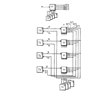
of known kind. Figure 3 illustrates an inventive selector memory
device SS. Data information entering the selector memory device SS
is distributed on incoming time slots. The data information enters
on an input IN. The in-coming data information is written-in
cyclicly, in the same manner as data is Written into the earlier
known selector memory device described above. The write-in of
information takes place during a write phase of a time slot
interval, as earlier described.
The inventive selector memory device is equipped with a plurality
of outputs 0UT0,...0UT3, according to the illustrated embodiment
four outputs. Connected to the selector memory device SS are an
equal number of control memory devices CSO,...CS3 corresponding
to respective outputs. The control memory devices contain con-
trol information for controlling the read-out of data information
from the selector memory device. In the illustrated example, the
outputs and control memory devices are numbered from 0 to 3. Each
of the control memory devices is connected to a corresponding
2044273
WO 91/0757 PCl'/SE90/OObbS
output for read-out purposes. With read-out to output number 0
OUTO, control memory device number 0 CSO is connected to control
the read-out. In the case of read-out to output number 1 OUT1, the
control memory device number 1 CS1 is connected to control the
read-out, and so on. In order to enable one single selector memory
device according to the invention to replace several selector
memory devices of known kind, several read-outs are effected
sequentially, each to a respective output, during a time slot
interval corresponding to an incoming time slot. Read-out takes
place during a read phase. In the case of the illustrated example,
one time slot interval includes four read phases, data information
being read-out to the output OUT number 0 during the first read
phase under the control of control information stored in the
control memory device CS number 0, data information being read to
the output number 1 during the second read phase of the time slot
interval, under the control of control information.contained in
the control memory device CS number 1 and so on. During a read
phase, the actual read-out is controlled in the same manner as in
known techniques. During the first read phase of a time slot
interval, for instance number 7, the control information in the
control memory device number 0, memory cell number 7, controls
which memory cell of the selector memory device data information
can be read from. Thus, the control information contains the
address in the selector memory device from which data information
can be read. In the case of the illustrated example, the time
interval includes a time slot, thus partly a write phase and
partly four read phases. The inventive selector memory therewith
replaces effectively four selector memory devices of known kind.
Thus, one advantage of using the inventive selector memory device
is found in the saving of memory space.
Figure 4 illustrates the selector core of a T-S-selector which is
of the same size as the selector core of the Figure 2 embodiment,
but which is constructed with selector memory devices according to
the invention. The gain obtained in the form of saved memory space
when using the inventive selector memory device instead of a known
selector memory device is clearly evident when a comparison is
made between these two selector cores. In the case of the selector
7 20442'3
WO 91/07857 PCT/S E90/00665
core illustrated in Figure 4, the number of selector memory
devices SS has been reduced to four, i.e. to a quarter of the
number of selector memory devices required in the Figure 2 em-
bodiment.
As with the earlier described selector core, the selector core of .
the Figure 4 embodiment includes four I/O-devices. The selector
core includes four inventive selector memory devices SS which are
arranged in a column, column number o. Each inventive selector
memory device SS replaces a row of known selector memory devices
in the earlier described T-S-selector. Data information from the
I/O-devices is supplied to the selector memory devices on incoming
lines 14, 15, 16, 17, and subsequent to time-slot-switching in the
selector memory devices the data information is delivered from the
outputs OUT 0, OUT 2, OUT 2, OUT 3 back to the I/O-devices on
outgoing data lines 24, 25, 26, 27.
The following takes place in the T-S-selector core illustrated in
Figure 4 during a time slot interval corresponding to an incoming
time slot, for instance time slot number 7. During the write
phase, data information from the I/O-devices is written into
memory cell number 7 in corresponding selector memory devices. The
time slot interval includes thereafter four read phases. During
the first read phase, control information in the memory cell
having address number seven in control memory device CS number 0
controls the read-out from one single selector memory device of
the column to I/O-device number 0 on the autgoing data line number
24 which is connected to output OUT number 0 on respective
selector memory devices SS. The control information partly
controls which of the selector memory devices is relevant for
read-out and partly controls from which memory cell in the
selector memory device concerned read-out shall be effected.
During the second read phase of the exemplifying time slot
interval, the read out from one of the selector memory devices is
controlled by control information in control memory device CS
number 1. The read out is then effected to I/O-device number 1 on
the output line 25 which is connected to output OUT number l on
respective selector memory devices. Read-out from the selector
;v<.. ~ v .;..., , v .. . .,,. . .', '. A,~ '. . . :
.. .. . . ;; : .: . " . , , . ;,
' . , ..
;:.
,
:
. : -. .. . .. ;. .,.:. , ",
,: . : ;
:, .
' ' '
: : ' v '
' '
~
. ... .
, . ;:
: ,
,. :: ~ ,
;;:
' .
1
~
~f :w ~. . : ; ,. '. ,
. ' ;.; . ,
/
204427
WO 91 /07857 PCT/SE90/00665
memory devices takes place in the same manner during the third
and fourth read phases, read-out during the third read phase is
controlled by control memory device number 2 and data information
is delivered to I/O-device number 2. The read-out during the
fourth read phase is controlled by control information in control
memory device CS number 3, data information being delivered to
I/O-device number 3. During the read phases of the time slot
interval, read-out is thus effected to all I/O-devices, with the
read-out to different I/O-devices taking place during separate
read phases of the time slot interval.
It is, of course, possible to extend the selector core with more
I/O-devices and more selector memory devices. For instance, if the
selector core is extended with a further four I/O-devices, the
number of selector memory devices increases to sixteen selector
memory devices arranged functionally in two columns of eight.
Information is written-in rowwise, so that the same data informa-
tion is written into the two selector memory devices belonging to
the same row. Data information is delivered to the selector memory
devices from the I/O-device which corresponds to respective rows
of selector memory devices. In read-out, data information is read
from one of the columns to four of the eight I/o-devices and from
the other column to the remaining four I/O-devices. Thus, read-
out from each column is effected to four I/O-devices corresponding
to said column, since the selector memory devices in respective
columns have four outputs and are controlled by four control
memory devices during four read phases of each time slot interval.
It will be seen that compared with known technique, each in°
dividual read-out effected in accordance with the invention will
take place more quickly than a read-out from known selector memory
devices, since a time slot interval corresponding to an incoming
time slot includes four read phases instead of only one, as in the
earlier known case. This rapid read-out of information enables the
number of selector memory devices required to be reduced when
using the inventive selector memory device.
204423
WO 91/07857 PC1"/SE90/OOu65
The aforedescribed, exemplifying selector memory device has four
read phases for each write phase and is connected to the same
number of control memory devices and therewith replaces four
selector memory devices of the earlier known kind. It is also
possible to construct an inventive selector memory device such
that said device will replace a number of known selector memory
devices other than four. For instance, the inventive selector
memory device can be constructed for two or eight read phases for
each write phase and can be connected to a corresponding number of
control memory devices. The factor which is capable of limiting
.. the number of control memory devices that can be connected to the .
selector memory device is found in the shortest possible read
out time, since it must be possible to effect during a time slot
interval the same number of read-outs as the number of control
memory devices.that are connected to a selector memory device.
Although not really preferred, it is conceivable in the case of
multiplexes to provide a selector memory device with fewer outputs . , .
than the number of read phases and the number of control memory
devices connected to the selector memory device. When demul
tiplexers are connected to the I/O-devices in a selector, it is
conceivable for more I/O-devices in time multiplex to share a line
or some other data transmission medium from the outputs of the
selector memory devices.