Note: Descriptions are shown in the official language in which they were submitted.
204~319
PATENT APPLICATION
Attorney's Docket No. D/891 14
BACKGROUND OF THE INVENTION
This invention relates generally to the rendering of latent
electrostatic images visible using multiple colors of dry toner or developer
and, more particularly, to a high speed, highlight printer which exhibits
high copy quality without degradation of process speed.
The invention can be utilized in the art of xerography or in
related printing arts. In the practice of conventional xerography, it is the
general procedure to form electrostatic latent images on a xerographic
surface by first uniformly charging a photoconductive insulating surface or
photoreceptor. The charge is selectively dissipated in accordance with a
pattern of activating radiation corresponding to original images. The
selective dissipation of the charge leaves a latent charge pattern on the
imaging surface corresponding to the areas not struck by radiation.
This charge pattern is made visible by developing it with toner.
The toner is generally a colored powder which adheres to the charge
pattern by electrostatic attraction.
The developed image is then fixed to the imaging surface or is
transferred to a receiving substrate such as plain paper to which it is fixed
by suitable fusing techniques.
Multi-color imaging has also been accomplished utilizing basic
xerographic techniques. In this instance, the foregoing process is essentially
repeated for three or four cycles. Thus, the charged photoconductive
surface is successively exposed to filtered light images. After each exposure
the resultant e~ectrostatic latent image is then developed with toner
particles corresponding in color to the subtractive primary of the filtered
light image. For example, when a red filter is employed, the electrostatic
latent image is developed with toner particles which are cyan in color. The
cyan toner powder image is then transferred to the copy sheet. The
foregoing process is repeated for a green filtered light image which is
204~319
-
developed with magenta toner particles and a blue filtered light image
which is developed with yellow toner particles.
Each differently colored toner powdered image is sequentially
transferred to the copy sheet in superimposed registration with the powder
image previously transferred thereto. In this way, three or more toner
powder images are transferred sequentially to the copy sheet. After the
toner powder images have been transferred to the copy sheet, they are
permanently fused thereto. The foregoing color imaging process is known
as full color imaging.
Another color imaging process is known as highlight color
imaging. In highlight color imaging two different color developers are
customarily employed, usually black and some other color, for example,
red. In one type of highlight color imaging, a tri-level image is formed on
the imaging surface utilizing a three level ROS (Raster Output Scanner) to
form the tri-level image on a charge retentive surface that had previously
been uniformly charged . The tri-level image comprises two image areas
and a background area.
The concept of tri-level xerography is described in U.S. Patent
No. 4,078,929 issued in the name of Gundlach. The patent to Gundlach
teaches the use of tri-level xerography as a means to achieve single-pass
highlight color imaging. As disclosed therein, the charge pattern is
developed with toner particles of first and second colors. The toner
particles of one of the colors are positively charged and the toner particles
of the other color are negatively charged. In one embodiment, the toner
particles are supplied by a developer which comprises a mixture of
triboelectrically relatively positive and relatively negative carrier beads. Thecarrier beads support, respectively, the relatively negative and relatively
positive toner particles. Such a developer is generally supplied to the
charge pattern by cascading it across the imaging surface supporting the
charge pattern. In another embodiment, the toner particles are presented
to the charge pattern by a pair of magnetic brushes. Each brush supplies a
toner of one color and one charge. In yet another embodiment, the
204~319
-
.~
development system is biased to about the background voltage. Such
biasing results in a developed image of improved color sharpness.
In tri-level xerography, the xerographic contrast on the charge
retentive surface or photoreceptor is divided three, rather than two, ways
as is the case in conventional xerography. The photoreceptor is charged,
typically to 900v. It is exposed imagewise, such that one image
corresponding to charged image areas (which are subsequently developed
by charged area development, i.e. CAD) stays at the full photoreceptor
potential (Vddp or Vcad, [see Figures 1a and 1b]). The other image is
exposed to discharge the photoreceptor to its discharge potential, i.e. Vc or
Vdad (typically 100v) which corresponds to discharged area images that are
subsequently developed by discharged-area development (DAD). The
background areas exposed such as to reduce the photoreceptor potential
to halfway between the Vcad and Vdad potentials, (typically 500v) and is
referred to as Vw or VWhite. The CAD developer is typically biased about
1 OOv closer to Vcad than VWhite (about 600v), and the DAD developer system
is biased about 1 OOv closer to Vdad than VWhite (about 400v).
Because the composite image developed on the charge retentive
surface consists of both positive and negative toner a pre-transfer corona
charging step is necessary to bring all the toner to a common polarity so it
can be transferred using corona charge of the opposite polarity.
As will be appreciated, a highlight color printer which is capable
of a high degree of copy quality at a relatively high process speed is quite
desirable. However, to date no acceptable system that incorporates both of
these characteristics has been identified. Considered have been two pass
highlight color systems using insulative magnetic brush (IMB) black
development which would satisfy the goal of high quality and single pass
systems (Tri-level Xerography) which would satisfy the latter goal but with
a compromise in black copy quality.
Various techniques have heretofore been employed to create
and develop electrostatic images as illustrated by the following disclosures
which may be relevant to certain aspects of the present invention.
2044319
U.S. Patent No. 4,761,668 granted to Parker et al and assigned to
the same assignee as the instant application which relates to tri-level
printing discloses apparatus for minimizing the contamination of one dry
toner or developer by another dry toner or developer used for rendering
visible latent electrostatic images formed on a charge retentive surface such
as a photoconductive imaging member. The apparatus causes the
otherwise contaminating dry toner or developer to be attracted to the
charge retentive surface in its inter-document and outboard areas. The dry
toner or developer so attracted is subsequently removed from the imaging
member at the cleaning station.
U.S. Patent No. 4,761,672 granted to Parker et al and assigned to
the same assignee as the instant application which relates to tri-level
printing discloses apparatus wherein undesirable transient development
conditions that occur during start-up and shut-down in a tri-level
xerographic system when the developer biases are either actuated or de-
actuated are obviated by using a control strategy that relies on the
exposure system to generate a spatial voltage ramp on the photoreceptor
during machine start-up and shut-down. Furthermore, the development
systems' bias supplies are programmed so that their bias voltages follow the
photoreceptor voltage ramp at some predetermined offset voltage. This
offset is chosen so that the cleaning field between any development roll
and the photoreceptor is always within reasonable limits. As an alternative
to synchronizing the exposure and developing characteristics, the charging
of the photoreceptor can be varied in accordance with the change of
developer bias voltage.
U.S. Patent No. 4,811,046 granted to Jerome E. May and assigned
to the same assignee as the instant application which relates to tri-level
printing discloses apparatus wherein undesirable transient development
conditions that occur during start-up and shut-down in a tri-level
xerographic system when the developer biases are either actuated or de-
actuated are obviated by the provision of developer apparatuses having
rolls which are adapted to be rotated in a predetermined direction for
preventing developer contact with the imaging surface during periods of
- 2044~19
.~,,
start-up and shut-down. The developer rolls of a selected developer
housing or housings can be rotated in the contact-prevention direction to
permit use of the tri-level system to be utilized as a single color system or
for the purpose of agitating developer in only one of the housings at a time
to insure internal triboelectric equilibrium of the developer in that housing.
U.S. Patent No 4,771,314 No. granted to Parker et al and
assigned to the same assignee as the instant application which relates to tri-
level printing discloses printing apparatus for forming toner images in
black and at least one highlighting color in a single pass of a charge
retentive imaging surface through the processing areas, including a
development station, of the printing apparatus. The development station
includes a pair of developer housings each of which has supported therein a
pair of magnetic brush development rolls which are electrically biased to
provide electrostatic development and cleaning fields between the charge
retentive surface and the developer rolls. The rolls are biased such that the
development fields between the first rolls in each housing and the charge
retentive surface are greater than those between the charge retentive
surface and the second rolls and such that the cleaning fields between the
second rolls in each housing and the charge retentive surface are greater
than those between the charge retentive surface and the first rolls.
U.S. Patent No. 4,833,504 No. granted to Delmer Parker and
assigned to the same assignee as the instant application which relates to tri-
level printing discloses a magnetic brush developer apparatus comprising a
plurality of developer housings each including a plurality of magnetic rolls
associated therewith. The magnetic rolls disposed in a second developer
housing are constructed such that the radial component of the magnetic
force field produces a magnetically free development zone intermediate a
charge retentive surface and the magnetic rolls. The developer is moved
through the zone magnetically unconstrained and, therefore, subjects the
image developed by the first developer housing to minimal disturbance.
Also, the developer is transported from one magnetic roll to the next. This
apparatus provides an efficient means for developing the complementary
half of a tri-level latent image while at the same time allowing the already
developed first half to pass through the second housing with minimum
image disturbance.
U.S. Patent No. 4,901,114 issued on February 13, 1990 in the
name of Parker et al and assigned to the same assignee as the instant
application which relates to tri-level printing discloses an electronic printer
employing tri-level xerography to superimpose two images with perfect
registration during the single pass of a charge retentive member past the
processing stations of the printer. One part of the composite image is
formed using Magnetic Ink Character Recognition ( MICR ) toner, while the
other part of the image is printed with less expensive black, or color toner.
For example, the magnetically readable information on a check is printed
with MICR toner and the rest of the check in color or in black toner that is
not magnetically readable.
U.S. Patent No. 4,868,611 issued in the name of Richard P.
Germain on September 19, 1989 discloses a highlight color imaging method
and apparatus including structure for forming a single polarity charge
pattern having at least three different voltage levels on a charge retentive
surface wherein two of the voltage levels correspond to two image areas
and the third voltage level corresponds to a background area. Interaction
between developer materials contained in a developer housing and an
already developed image in one of the two image areas is minimized by the
use of a scorotron to neutralize the charge on the already developed
image.
U.S. Patent No. 4,562,130 granted to Tateki Oka on
December31, 1985 discloses a method of forming composite images
wherein a first electrostatic latent image of positive image is formed on a
photosensitive member after which a scorotron charger is used to correct
the potential of the background area to an intermediate potential. This is
followed by the formation of a second latent image by exposing the
intermediate potential to a negative image.
U.S. Patent No. 4,959,286 granted to Charles Tabb on
September 25, 1990 discloses an imaging method and apparatus
utilizing some of the features of both single and two pass
20~319
highlight color imaging. Both developer housings are always actively
engaged. One housing is used for charged area development (CAD) and
the other is used for discharged area development (DAD). The developer
housing biases are switched or adjusted in order to preclude unwanted
image development. When the DAD image moves through the CAD
housing the CAD bias is switched to bias away the developer in the CAD
developer housing. Likewise, when the CAD image moves through the
DAD housing its bias will be switched to bias away the DAD developer.
BRIEF SUMMARY OF THE INVENTION
In accordance with the present invention there is disclosed a
single pass printer which utilizes two imaging systems for forming latent
electrostatic images on charge retentive belt photoreceptor. After the
charge retentive belt is uniformly charged, a 600 SPI Raster Output Scanner
(ROS) or other device in a "write black" mode forms a bi-level (i.e.
background and image areas) latent electrostatic image. The bi-level
image is then developed using an Insulated Magnetic Brush (IMB), HAZE
(Highly Agitated Zone), MAZE (Magnetically Agitated Zone) or other "high
~ resolution" development system using Discharge Area Development (DAD)
with negative black toner and positive carrier. The next step comprises
forming a second image with a Dlow UMC (unit manufacturing cost) 300
spi imaging device which images in the write white mode exposing all non-
developed charged areas except those to be developed in color. This
photodischarge step is of an "intermediate exposure" designed to
photodischarge the background area of the original bi-level image to a
voltage level comparable to the partially neutralized black image. This
second imaging step is followed by a second development step as the
image passes through a second development housing. The second
development housing is a tri-level type housing (i.e. multi-roll, Conductive
Magnetic Brush (CMB) development system that exhibits a low
development field. The second development housing contains a positive
charging color toner and negative carrier.
- 7a -
According to one aspect of the present invention there is provided a method of
forming plural images, the method including the steps of a:
uniformly charging a charge retentive belt;
using a 600 spi ROS, discharging portions of the uniformly charged retentive
belt to form relatively high and low voltage areas of the same polarity on the belt;
providing a high resolution development system;
providing an electrical bias for the development system such that a relatively
large development field is provided between a developer structure forming a part of
the development system and the relatively low voltage areas,
using the high resolution development system, developing the areas of
relatively low voltage with first toner material contained in the developer structure;
using a 300 spi LED, discharging portions of the relatively high voltage areas
of the charge retentive belt to form areas at a voltage level intermediate the relatively
high and low voltage areas; and
developing the rem~ining areas of high voltage level with a second toner
material which is distinct and of opposite polarity from the first toner material leaving
the intermediate voltage background level undisturbed.
According to another aspect of the present invention there is provided an
apparatus for forming plural images using a charge retentive belt, the apparatus
compnsmg:
means for uniformly charging the belt;
a 600 spi ROS for discharging portions of the uniformly charged retentive belt
to form relatively high and low voltage areas of the same polarity on the belt;
a high resolution development system for developing the areas of relatively
low voltage with a first toner;
means for electrically biasing of the development system such that a relatively
large development field is provided between a developer structure forming a part of
the development system and the relatively low voltage;
a 300 spi LED for discharging portions of the relatively high voltage areas of
the charge retentive belt to form areas at a voltage level intermediate the relatively
high and low voltage areas; and
.,, ,~
- 7b -
means for developing the areas of high voltage level with a second toner
material which is distinct from the first toner material.
s
204~319
DESCRIPTION OF THE DRAWINGS
Figure 1a is a plot of photoreceptor potential versus exposure
illustrating a tri-level electrostatic latent image;
Figure 1 b is a plot of photoreceptor potential illustrating single-
pass, highlight color latent image characteristics;
Figure 2 is schematic illustration of a printing apparatus
incorporating the inventive features of our invention;
Figure 3a depicts the voltage profile on a charge retentive
surface after a first exposure step;
Figure 3b depicts the charge retentive surface of Figure 3a after
development of the first image formed by the first exposure step;
Figure 3c depicts the charge retentive surface subsequent to a
second exposure step; and
Figure 3d depicts the charge retentive surface after a second
development step.
DETAILED DESCRIPTION OF THE PREFERRED
EMBODIMENT OF THE INVENTION
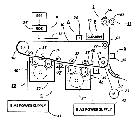
As shown in Figure 2, a printing machine incorporating the
invention utilizes a charge retentive member in the form of a
photoconductive belt 10 consisting of a photoconductive surface and an
electrically conductive substrate and mounted for movement past a
charging station A, an exposure station B, developer station C, transfer
station D and cleaning station F. Belt 10 moves in the direction of arrow 16
to advance successive portions thereof sequentially through the various
processing stationsdisposed aboutthe path of movementthereof. Belt 10
is entrained about a plurality of rollers 18, 20 and 22, the former of which
can be used to provide suitable tensioning of the photoreceptor belt 10 and
the latter of which can be used as a drive roller. Motor 23 rotates roller 20
to advance belt 10 in the direction of arrow 16. Roller 20 is coupled to
motor 23 by suitable means such as a belt drive.
20~319
..~,
As can be seen by further reference to Figure 2, initially
successive portions of belt 10 pass through charging station A. At charging
station A, a corona discharge device such as a scorotron, corotron or
dicorotron indicated generally by the reference numeral 24, charges the
belt 10 to a selectively high uniform predetermined negative potential.
Alternatively, the belt may be charged to a uniform predetermined positive
potential. Any suitable control, well known in the art, may be employed
for controlling the corona discharge device 24.
Next, the uniformly charged portions of the photoreceptor
surface are advanced through exposure station B. At exposure station B,
the uniformly charged belt photoreceptor or charge retentive surface 10 is
exposed to a laser based input and/or output scanning device 25 which
causes the charge retentive surface to be discharged to form bi-level
images, each comprising a background level Vbkg DAD of about -700 volts
and a discharged image area, Vima9e DAD of approximately -100 volts
(Figure 3a). The scanning device 25 is a two level, 600 Spots Per Inch (SPI)
Raster Output Scanner (ROS). Other exposure devices such as LED bars may
be employed in lieu of the device 25
At development station C, a magnetic brush development
system, indicated generally by the reference numeral 30 advances
developer materials into contact with electrostatic latent images on the
photoreceptor. The development system 30 comprises first and second
developer housings 32 and 34. Preferably, each magnetic brush
development housing includes a plurality of magnetic brush developer
rollers. Thus, the housing 32 contains a pair of rollers 35, 36 while the
housing 34 contains a pair of magnetic brush rollers 37, 38. Each pair of
rollers advances its respective developer material into contact with the
latent image. Appropriate developer biasing is accomplished via power
supplies 41 and 43 electrically connected to respective developer housings
32 and 34.
The discharged area, Vjmage DAD of the bi-level image is
developed using an Insulated Magnetic Brush (IMB), HAZE (Highly Agitated
Zone), MAZE (Magnetically Agitated Zone) or other nhigh resolution"
development system using Discharge Area Development (DAD) with negative black
toner and positive carrier contained in the housing 32. A Haze or Maze development
5 system consists of the photoreceptor belt 10 urged into intim~te contact with rollers 35
and 36 to effect the agitated zone. The photoreceptor voltage profile and development
black image are illustrated in Figure 3b. For proper development of the bi-levelimage, the developer rolls 32 and 34 are electrically biased to voltage, Vdev bias DAD
equal to approximately -600 volts. With such biasing of the developer rollers, a10 relatively large development field, Vdev field DAD iS provided
Subsequent to development of the bi-level image, a second image is formed
with a "low I~MC" (unit manufacturing cost) 300 spi im;~ging device, for example a
light emitting diode (LED) array 48 disposed intermediate the developer housings 32
and 34. The im~ging device 48 discharges all non-developed charged areas of the bi-
15 level image except those to be developed in colour. This results in a second bi-level
image (Figure 3c) comprising a discharged area voltage level, Vbkg CAD of
approximately -350 volts and an image area voltage level, Vimage CAD of approximately
-700 volts. This photodischarge step is of an "intermediate exposure" designed to
photodischarge the background area of the original bi-level image to a voltage level
20 comparable to the partially neutralized black image.
The second imaging step is followed by a second development step as the
image passes through the second development housing 34. The second development
housing is a tri-level type housing (i.e. multi-roll, Conductive Magnetic Brush (CMB)
development system that exhibits a low development field. It contains a positive25 charging colour toner and negative carrier. For development of the coloured image,
the developer rolls 37 and 38 are electrically biased to a voltage of approximately
-450 volts resulting in a relatively small development field, Vdev field CAD The voltage
profile of both the developed black and colour images are depicted in Figure 3d.Because the composite image developed on the photoreceptor consists of both
30 positive and negative toner, an erase member indicated by reference character 45
together with a suitable pre-transfer corona
2Q~4319
~,
discharge member 56 using either negative or positive corona discharge are
provided to condition the toner for effective transfer to a substrate .
A sheet of support material 58 (Figure 2) is moved into contact
with the toner image at transfer station D. The sheet of support material is
advanced to transfer station D by conventional sheet feeding apparatus,
not shown. Preferably, the sheet feeding apparatus includes a feed roll
contacting the uppermost sheet of a stack of copy sheets. Feed rolls rotate
so as to advance the uppermost sheet from stack into a chute which directs
the advancing sheet of support material into contact with photoconductive
surface of belt 10 in a timed sequence so that the toner powder images
developed thereon contact the advancing sheet of support material at
transfer station D.
Transfer station D includes a corona generating device 60 which
sprays ions of a suitable polarity onto the backside of sheet 68. This attracts
the charged toner powder images from the belt 10 to sheet 58. After
transfer, the sheet continues to move, in the direction of arrow 62, onto a
conveyor (not shown) which advances the sheet to fusing station E. A
detack corona generating device (not shown) may also be employed.
~ Fusing station E includes a fuser assembly, indicated generally by
the reference numeral 64, which permanently affixes the transferred
powder image to sheet 58. Preferably, fuser assembly 64 comprises a
heated fuser roller 66 and a backup roller 68. Sheet 58 passes between
fuser roller 66 and backup roller 68 with the toner powder image
contacting fuser roller 66. In this manner, the toner powder image is
permanently affixed to sheet 58. After fusing, a chute, not shown, guides
the advancing sheet 58 to a catch tray, also not shown, for subsequent
removal from the printing machine by the operator.
After the sheet of support material is separated from
photoconductive surface of belt 10, the residual toner particles carried by
the non-image areas on the photoconductive surface are removed
therefrom. These particles are removed at cleaning station F. A cleaner
housing 70 is disposed at the cleaner station F. The cleaning station F also
may contain a pre-clean corona device, not shown.
20g~319
Subsequent to cleaning, a discharge lamp (not shown) floodsthe
photoconductive surface with light to dissipate any residual electrostatic
charge remaining prior to the charging thereof for the successive imaging
cycle.