Note: Descriptions are shown in the official language in which they were submitted.
204~376
ELECTRON SOURCE WITH MICRDDOT EMI _ VE CATHODES
DESC~IPTIQN
m e present invention relates to a mic mdot emissive cathode electrDn
source and to its production process. It more partiaularly applies to
the production of flat display screens.
French patents 2 593 953 and 2 623 013 disclose display means by
cathadoluminescence excited by field emission and which incorporate a
microdot emissive cathode electron source.
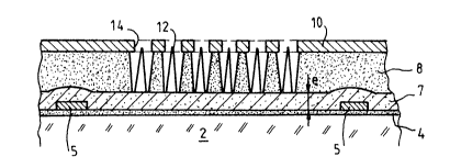
Fig. l diagramnatically shows a known micm dot emissive cathode elec-
tron saurce described in detail in French patent 2 623 013. This
source has a matrix structure and aptionally comprises an an e.g. glass
substrate 2, a thin silica film 4. On the latter are fonmed a plur-
ality of electrodes 5 in the form of parallel conductive strips se~ving
as cathode canductors and constituting the columns of the matrix struc-
ture. Each of the cathode ca,nductors is covered by a resistive ca,ating
7, which can be continuaius (except at the ends in order to permit the
connection of the cathode conductors to the polarizing means 20).
An electrically insulating layer 8, made fm m silica, ca,versi the resis-
tive coating 7. Above the insulating layer 8 are forned a plurality of
electrodes 10, a,nce again in the form of parallel conductive strips.
These electrcdes 10 are perpendicular to the electm des 5 and serve as
grids, which constitute the rows of the matrix structure.
The knawn source also has a plurality of elementary electron emitters
(mic m dots), ane of which is diagrammatically shawn in fig. 2. In each
of the intersection zones of the cathode conductors 5 and the grids 10,
the resistive coating 7 corIesponding to said zone supports e.g.
molybdenum microdots 12 and the grid 10 corresponding to said zone has
an cpening 14 facing each of the microdots 12. Each of the latter
substantially adopts the sllape of a cone, whose base rests on the
coating 7 and whose apex is level with the corresponding opening 14.
Obviously, the insulating layer 8 also has openings 15 penmitting the
passage of the microdots 12.
B 10443.3 AM
~,
20~437S
-- 2 --
For information, the following orders of magnitude are given:
thickness of insulating layer 8: 1 micrometer,
thickness of a grid 10: 0.4 micrometer,
diameter of an opening 14: 1.4 micrometer,
diameter of a base of a microdot 12: 1.1 micrometer,
thickness of a cathode conductor 5: 0.2 micrometer,
thickness of a resistive coating: 0.5 micrometer.
The essential object of the resistive coating 7 is to limit the current
in each emitter 12 and consequently to homogenize the electron emis-
sion. In an application to the excitation of spots (pixels) of a dis-
play screen, this makes it possible to eliminate the excessively bright
dots.
The resistive coating 7 also makes it possible to reduce breahdown risk
at the microdots 12 through limiting the current and thus preventing
the appearance of short-circuits between rows and columns.
Finally, the resistive ooating 7 allows the short-circuiting of a few
emitters 12 with a grid 10, the very limited leakage current (a few yA)
in the short-circuits not disturbing the cperation of the renainder of
the cathode conductor. Unfortunately, the problem caused by the appear-
ance of short-circuits between the microdots and a grid is not solved
in a satisfactory manner by a device of the type described in French
patent 2 623 013.
Fig. 3 diagra~matically shows a microdot. A metal particle 16 causes a
short-circuit of the microdot 12 with a grid 10 and in this case all
the voltage applied between the grid 10 and the cathode conductor 5
(Vcg approximately 100 Vj is transferred to the terminals of the
resistive coating 7.
In order to be able to accept a few short-circuits of this type and
which are virtually inevitable due to the very large number of micro-
dots, the resistive coating 7 must be able to withstand a voltage close
B 10443.3 AM
2044376
-- 3 --
to 100 V, which requires its thickness to exceed 2 ~m. In the oppositecase, it would lead to a brea~down due to the heat effect and a con-
plete short-cirsuit would appear between the grid and the cathode
conductor making the electron source unusable.
The present invention obviates this disadvantage. It aims at i~provingthe breakdown resistance of an electron source having microdot emissive
cathodes, said improvement being obtained without increasing the thick-
ness of the resistive source.
In order to achieve this objective, the invention recommends the use ofelectrcdes (e.g. cathcde conductors) in grating form in such a way that
these electrcdes and the associated resistive coatings are substan-
tially in the same plane. In this configuration, the breakdown resis-
tance is no lalger dependent (primarily) on the thickness of the resis-
tive coating, but instead on the distance between the cathode conductor
and the micrcdot. It is therefore sufficient to maintain a sufficient
distance between the cathode conductor and the microdot to prevent
breakdown, whilst still retaining a homcgenization effect for which the
resistive coating is provided.
More specifically, the present invention relates to an electron source
incorporating, on an insulating support, a first ~series of parallel
electrodes serving as cathode conductors and carrying a plurality of
microdots made from an electron emitting material and a second series
of parallel electrcdes, serving as grids and which are electrically
insulated from the cathode conductors and forming an angle therewith,
which defines intersection zones of the cathode conductors and the
grids, the grids having openings respectively facing the microdots.
Each of the electrodes of at least one of the series has a grating
structure in contact with a resistive coating.
In a preferred manner, the electrodes having a grating structure are
metallic and are e.g. of Al, Mo, Cr, Nb, etc. It also has an improved
B 10443.3 AM
2044376
conductivity. In a preferred manner, the size of a mesh of the grating
is less than the size of an intersection zone. Advantageously, an
intersection zone cover~ several grating meshes.
This assists the operation of the electron source for bwo reasons:
a) The nominal current per mesh decreases as the number of meshes
increases. When the cathode conductors have a grating structure, the
access resistance of a cathode conductor to all the microdots of a
mesh can be accepted in proportion to the number of meshes, which makes
it possible to reduce the leakage current in the case of a short cir-
cuit. Thus, the access resistance is not very dependent on the size of
the mesh and the number of mic m dots per mesh. It is mainly dependent
on the resistivity and thickness of the resistive coating.
b) The larger the number of meshes within an over~p zone, the less
the non-operation (short-circuit) of a mesh disturbs the cperation of
the electron source. (In the case of an application to the excitation
of a screen, only a fraction of a pixel is extinguished for a defective
mesh, which is not visible on the screen).
The meshes of the grating can have a random shape and can e.g. be
rectangular or square. According to a preferred embodiment, the gra-
ting meshes are square. According to a variant, the catho e conductors
have a grating-like structure.
In this case, advantageously, the micrcdots occupy the central regions
of the grating meshes. This arrangement makes it possible to pr~vide
an adequate distance between a cathode conductor and the microdots to
prevent breakdown.
According to a development of this variant, each cathode conductor is
covered by a resistive coating. According to another development, a
resistive coating is insertad between the insulating support and each
cathode oonductor.
B 10443.3 AM
20~376
The resistive coating can be made frcrn a material such as indiun oxide,
tin oxide or iron oxide. Preferably, the resistive coating is of do~ed
silicon.
Whatever material is chosen, it is necessary to ensure that the latter
has a resistivity adapted to the har~genization and short-circuit
protection effects. This resistivity generally exceeds 1021~ cm,
whereas the resistivity of the cathcde conductor is generally belcw
10 3l~ an.
In another constructional variant, the grids have a grating st_ucture.
In this case, the cathode conductors may or may not have a grating
structure. The resistive coating is no longer necessary, but can still
be present in order to maintain a hanogenization effect.
In a develcpment of this variant, each grid is covered by a second
resist?ve coating having openings facing the micrcdots. In a further
develo~nent of this variant, each grid rests on a second resistive
coating having cpenings facing the microdots.
The resistive coating can be made f mrn a material such as indium cxide,
tin oxide or iron oxide. Preferably, the resistive coating is of dcped
silicon.
No matter which material is chosen, it must be ensured that the latter
has a resistivity adapted to the hcmogenization and short-circuit
protection effects. This resistivity generally exceeds 10 ~ cm,
whereas the resistivity of the cathode conductor is generally belcw
10 3~ cm.
If all the grids and cathode conductors have a grating structure, the
meshes of the gratings preferably have the sarne dimensions.
m e invention is described in greater detail hereinafter relative to
non-limitative ernbodiments and the attached drawings, wherein shcw:
B 10443.3 AM
2044376
-- 6 --
Fig. 1, already described and relating to the prior art, diagram-
matically a microdot emissive cathode electrvn source.
Fig. 2, already described and relating to the prior art, diagram-
matically a partial, sectional view of a microdot emissive
cathode electron source.
Fig. 3, already described and relating to the prior art, diagram-
matically an electron emitter short-circuited with a grid.
Fig. 4 A diagraTmatic, partial, sectional view of a first e~bodiment
of an electron source acconding to the invention.
Fig. 5 A diagrammatic, partial, plan view of the embcdiment of fig. 4.
Fig. 6 A diagrammatic view of another embodiment of the invention.
Fig. 7 A diagrammatic view of another embodiment of the invention.
Fig. 8 A diagrammatic view of another e~bcdiment of the invention.
With reference to figs. 4 and 5, a description will ncw be given of an
electron source according to the invention. In this construction, the
cathode conductors 5 have a grating-like structure. The meshes of the
grating can have a random geometry. In the embodiments shcwn, the
grating meshes are square. The spacing of the mesh p is e.g. approx-
imately 50 micrometers and the width d of the conductive tracks forming
the grating is e.g. approximately 5 micrometers. These conductive
tracks are preferably metallic, e.g. of Al, Mo, Cr, Nb or the like. A
cathcde conductor 5 has a width of 400 micrometers, the cathode con-
ductors being separated from one another by a distance of approximately
50 microneters. It is therefore clear that an intersection zone of a
cathode conductor 5 and a grid 10 (of width 300 micr~meters) covers
several grating meshes. Under these conditions, each overlap zone of a
cathode conductor 5 with a grid 10 consists of 48 meshes. The non-
operation of a mesh due to short-circuits between the grid 10 and the
1~443.3 AM
:::
2044376
microdots cnly disturbs the overall system in a proportion of 1/48,
which has no significant effect.
The microdots 12 are brought together in the central zones of the
meshes and are connected to the cathode conductor 5 by an e.g. doped
silicon resistive coating 7. The distance a sel~arating each microdot
12 can e.g. be 5 micrometers. The distance r separating the microdots
12 from the conductive tracks of the grating forming a cathode conduc-
tor 5 n~st be adequate to ensure that under normal operating conditions
the voltage dr~p in the resistive coating 7 produces the aforementioned
homogenization effect. As the doped silicon resistive coating 7 has a
thickness of e.g. 0.5 micrometer, said distance r is at a minimum 5
micrometers for a voltage drop between 5 and 10 V under ncminal oper-
ating conditions. For example, the distance r is 10 micrometers.
Each mesh contains a ~umber n of microdots 12 with
n = ((p - d - 2r)/a + 1)2.
In the represented embcdiment, n is equal to 36.
In this embodirnent, the access resistance of the cathode conductor 5 to
all the microdots 12 is not very dependent on the size of the mesh and
the number of micrcdots contained therein. It is essentially depen-
dent on the resistivity and thickness of the resistive coating 7. For
a silicon resistive coating, the resistivity p is approximately 3 103
ohm cm and its thickness e is e.g. 0.5 micrometer.
The access resistance R can be approximately calculated on the basis of
the formula:
R ~ P
2~e
in which R is approximately 107 ohms, which is adequate to obtain a
3S voltage dr~p of apprDximately 10 V in the resistive coating 7.
B 10443.3 AM
20~376
-- 8 --
Under these conditions, in the case of a short-circuit between an
emitter 12 and the grid 10, the leakage current in a mesh is substan-
tially equal to 10 microamperes, which is acceptable, because it does
not deteriorate the operation of the electron source.
A process for producing such a device can e.g. involve the following
stages:
a) On an e.g. glass insulating substrate 2 oovered with a thin film 4
(of thickness 1000 ~) of SiO2 is deposite~, e.g. by cathode sputtering,
a metal coating (thickness 2000 ~) e.g. of Nb.
b~ A grating structure is prcduced in the metal coating, e.g. by
photolithography and reactive ionic etching. Therefore this structure
is produced w er the entire active surface of the electron source.
c) A resistive, doped silicon coating (thickness 5000 A) is deposited
e.g. by cathode sputtering.
d) The resistive coating and the metal coating are etched, e.g. by
photogravure and reactive ionic etching, so as to form conductive
columns (e.g. of width 400 micrometers and spaced by 50 micrcmeters).
e) The electron source is ccmpleted by prcducing an insulating layer,
the grid and the microdots in accordance with the stages e.g. described
in French patent 2 593 953 filed on the part of ~he present Applicant.
According to the invention, the microdots are only produced within the
meshes. A positioning of the microdots with respect to the meshes of
the cathode conductors is consequently necessary with an accuracy of
approximately + 5 micrometers.
According to an embodiment diagrammatically shown in fig. 6, the cath-
cde conductors 5 have a grating structure resting on a resistive
coating 7. In this configuration, a resistive coating 7 is conse-
quently placed between the insulating support (more particulArly the
B 10443.3 AM
- 204~376
- 3
coating 4) and each cathode conductor 5.
According to a variant shown in section in fig. 7, the cathode conduc-
tors 5 no longer have a grating structure and instead the grids have
such a structure.
According to a first e~bodiment, a second resistive coating 18, e.g. of
dcped silicon an,d having a resistivity of approximately 104 ohm cm an,d
a thickness of 0.4 micrometer, rests on the insulating layer 8. It has
openings 20 for the passage of the microdots 12.
The grids lOa in the form of a grating with square meshes rests on the
second resistive coating 18. The microdots 12 are placed within the
central zone of the grating meshes.
According to a second embc,diment, the second resistive coating 18
covers the grids lOb, which rest on the insulating layer 8.
In this variant, the grids can be of Nb and have a thickness of 0.2
micrometer. The width of each grid lOa or lOb can be 5 micm neters for
a mesh spacing of 50 mic m meters.
In both the first an~d second embodiments, the second resistive coating
18 provi,des a protection against short-circuits, the resistive coating
7 homogenizing the electron emission.
In this variant, the resistive coating 7 can be of doped silicon e.g.
having a resistivity of 105 ohm cm and a thickness of 0.1 micrometer.
The cathode conductors 5 can e.g. be of rTO (tin-doped indium oxide).
According to another variant dia~rammatically shown in section in fig.8, the grids and cathode conductors ~ve a square mesh grating struc-
ture. The meshes of the grids and the cathode conductors are then
superimposed. The conductive tracks fonming the meshes of the grids
and the cathode conductors face one another in the overlap zones.
B 10443.3 AM
2~4~376
_ 10 -
In the same way as hereinbefore, a second resistive coating 18 covers
each grid lOb or the grids lOa can also cover the second resistive
coating lOa.
With regards to the cathode conductors, the latter can be covered by
the insulating layer 7 (cathode conductor 5b) or can cover the same
(cathode conductor 5a).
Whichever variant is adopted, an electron ~ource having grating-like
electrodes makes it possible to reduce breakdown risks, whilst ensuring
a good homogenization of the electron emission. The grating structure
makes it possible to increase the access resistance of the microdots
to the cathode conductors without increasing the thickness of the
resistive caating.
B 10443.3 AM