Note: Descriptions are shown in the official language in which they were submitted.
i 204~72 :
1 6~446-509
BURST CONTROL CIRCUIT FOR
US~ IN TDMA COMMUNICATIONS SYSTEM -
- ',
~ACKGROUND OF THE INVENTION ~
The present lnventlon relates to a burst control clrcuit -
for use ln a tlme dlvlslon multiple access (TDMA) communications
system and, more partlcularly, to a burst control circult for use
in a narrow-band TDMA communlcatlons system ln whlch lt is requir-
ed for a carrler wave ln a burst form (burst signal) to have not
only gently sloped leading and trailing edges but also hlgh-speed
rlse and fall tlmes.
~ conventlonal burst control clrcult ls known. The
known burst control clrcult lncludes a power ampllfler preceded by
an lnput level control clrcuit. A detector clrcult detects the
output level of the power ampllfier to produce a detected slgnal.
The burst control circult also lncludes a control signal generator
whlch generates a reference slgnal havlng gently sloped leadlng ~:
; ~:
~ and
`~.
X
,;,.~: .. . ~ . ., . , .. : ; ~
2- 20~672 ~: ;
trailing edges. The detected and reference signals are
voltage compared by a comparator to produce an error signal
indicating a voliage difference therebetween. Based on ~;
the error signal, two driver circuits control the output
levels of the input level circuit and the power amplifier,
respectively. By the above-mentioned configuration, the
power amplifier produces an output burst signal having
gently sloped leading and trailing edges, so that it
prevents unnecessary expansion of the spectrum of the
output burst signal which may otherwise interfer with
other burst signals.
Since the conventional burst control circuit mentioned
above controls both the levels of the input level control
circuit and the power amplifier, its output burst signal
can have an ON/OFF ratio high enough to meet a strict
standard, such as a standard set by the Group Special
Mobile (GSM) pan-European mobile telephone system. The `
conventional burst control circuit, however, would not
- produce an output burst signal having rise and fall times
quick enough to meet the standard of, for example, about
20 microseconds required by the GSM system. This can be
caused by the slow response speed of a control loop
`~ including the input level control circuit, power amplifier,
! detector circuit, comparator and two driver circuits. The
25 response speed of the control loop may be increased by the ~ ;
use of specially fabricated high-gain comparator and driver
~' '. -
':',~,.
3 _ 2 0`4 4 6 72
circuits. But, this is disadvantageous from the economical
viewpoint.
SUMMARY OF THE INVENTION
An object of the present invention is, therefore, to
provide a generally improved burst control circuit for use
in a TDMA communications system.
Another object of the present invention is to provide
a burst control circuit capable of producing an output
burst signal having high speed rise and fall times without
resorting to specially fabricated high-gain comparator
and driver circuits.
Still another object of the present invention is to
provide a burst control circuit capable of producing an
output burst signal having a high ON/OFF ratio, which may
meet strict standards, such as a GSM standard.
Yet another object of the present invention is to
provide a burst control circuit capable of controlling
the waveform of an output burst signal with a baseband ~-
signal alone. -~
According to the present invention, there is provided
a burst control circuit for use in a TDMA communications
:
system, comprising: power amplifier means having first
and second control terminals for amplifying an input
; burst signal to produce an output burst signal, the
amplifier means changing the level and waveform of the
_ 4 204 1672
output burst signal in response to level and waveform
control signals which are supplied through the first and
second terminals, respectively; ALC circuit means for
generating a level control signal on the basis of a signal
representing a difference between a first reference voltage
and the level of the output burst signal, and supplying
the generated level control signal to the first control
terminal as the level control signal; and waveform control
circuit means for generating a waveform control signal in
response to a burst timing signal, and supplying the
generated waveform control signal to the second control
terminal as the waveform control signal.
BRIEF DESCRIPTION OF THE DRAWINGS
The above-mentioned and other objects, features and
advantages of the present invention will become more
~ apparent from the following detailed description taken
; in conjunction with the accompanying drawings, in which:
~-~ Fig. l is a block diagram illustrating a burst control ''-
circuit according to a first preferred embodiment of the
present invention;
;~ I , -.
Figs. 2A - 2G show waveforms for explaining the
:~;: '- ' -.
operation of Fig. l circuit; ' ;
Fig. 3 is a block diagram illustrating the power ,
amplifier in the Fig. l circuit;
Fig. 4 is a block diagram illustrating the automatic
gain control (ALC) circuit in the Fig. l circuit;
20~4672
-- 5
Fig. 5 is a block diagram illustrating the waveform
control circuit in the Fig. 1 circuit; and
Fig. 6 is a block diagram illustrating a burst control
circuit according to a second preferred embodiment of the
present invention.
DETAILED DESCRIPTION OF THE PREFERRED EMBODIMENTS
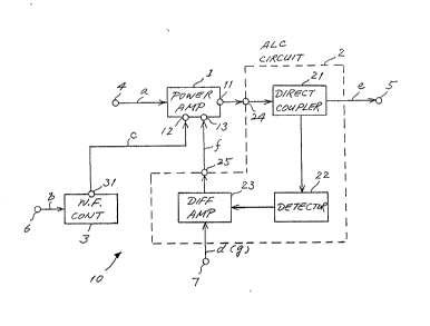
In Fig. 1, a burst control circuit 10 comprises a
power amplifier l to which a burst signal a is applied
through an input terminal 4 and from which a waveform-
and level-controlled burst signal _ is outputted through
an automatic level control ~ALC) circuit 2 and an output
~; terminal 5. The burst control clrcuit 10 may be used in
a TDMA communications system under the GSM standards in
which the carrier frequency of the input burst signal a
; 15 is in a 950 MHz band, and the duration of same lasts
about 600 microseconds, and the rise and fall times of
the output burst signal b have to be about 20 microseconds.
The power amplifier 1 has two control terminals 12
and 13 to which a waveform control signal c from a waveform
control circuit 3 and a level control signal f from the
l~ ALC circuit 2 are applied, respectively. These control
¦ signals c and f control the amplification factor of the
¦;; power amplifier 1 to thereby control the waveform and
level of the amplifier's output appearing at a terminal ll.
, 25 The output thus waveform- and level-controlled is outputted
~S~;r ;,'~ ' ' ~ .: .' i : .
- 20~4672 :~
.. - 6 -
to the output termina]. 5 as an output burst signal e through
the ALC circuit 2.
The ALC circuit 2 includes a directional coupler 11,
for deriving a part of the output burst signal. A detector
22 detects the level of the derived output burst signal to
produce and provide a detected burst level to a differential
amplifier 23. The differential amplifier 23 is also
provided with a reference signal d through a terminal 7
and compares the detected burst level with the voltage Vl
of reference signal d. The differential amplifier 23
increases its output when the detected burst level is
lower than the reference voltage Vl while decreasing its
output when the detected burst level is higher than the '.-.;
reference voltage Vl. The output of differential amplifier
13 is supplied to the power amplifier 1 as a level control
signal through control terminals 25 and 13. Applying the ~ -~
level control signal to the power amplifier 1 constitutes '
~ negative feedback to the amplifier 1. Thus, the output ~ .
`~ burst signal e has a level determined by the reference
voltage Vl and by the circuit constants of the power
amplifier 1 and of the ALC circuit 2.
The waveform control circuit 3 generates a waveform ~
control signal c in response to a burst timing signal b. .-
The waveform control signal c has gently sloped leading
25 and trailing edges and is applied to the power amplifier 1 .
through terminals 31 and 12. Thus, the output burst
_ 7 2~44672
signal e has gently sloped leading and trailing edges.
The periods of the leading and trailing edges, i.e., the
rise and fall times of the output burst signal e are
determined by those of the waveform control signal c.
It should be noted that the timing and duration of the
burst timing signal b is usually known in advance at a
station in whïch the burst control circuit 10 is installed.
In the Fig. 1 circuit, since the waveform control
signal c passes through no loop circuit, the rise and
fall times of the burst signal e can be shortened without
resorting to a specially fabricated cixcuit. Also, since
the control signal c is handled in a baseband, it is
relatively ease to handle it.
While in Fig. 1 the power amplifier 1 is supposed
to have a characteristic that its output level rises with
., .
~ increases in the levels of the control signals c and f
,,~
inputted to the terminals 12 and 13, the output level of
.
power amplifier 1 may fall with increases in the levels
of control signals c and f. In this case, the ALC
20 circuit 2 and the waveform control circuit 3 have to -
output control signals having the polarities reverse
to those of the control signals c and f.
The operation of the embodiment of Fig. 1 will now
be described in further detail with reference to Figs.
2A to 2G. Assume that the input burst signal a ~Fig. 2A)
whose envelope manifests a rectangular waveform is inputted -
204~672
~ -- 8 --
to the input terminal 4 from time t2 till time t5. The
burst timing signal _ (Fig. 2B) is supplied to the waveform
control circuit 2 through the terminal 6 from tl, ahead
of time t2, till time t4, ahead of time t5. The waveform
control circuit 2 responds to the inputted burst timing
signal b at time tl to start raising the voltage of
waveform control signal c (Fig. 2C) from zero and to
continue to raise it until it reaches a voltage Vw at
time t3, past time t2. Then, the waveform control
circuit 2, after holding the voltage of the waveform
control signal c at the constant level Vw, lowers it
from time t4 on until it converges to zero volt at time
t6, past time t5. ~ `
The reference voltage d (Fig. 2D) has a predetermined
~; 15 level Vl and is fed to the ALC circuit 2 from time t2
till time t5. The output level of power amplifier 1 is
substantially proportional to the product of the level
of level control signal f (Fig. 2F) and the level of the
~ , , .
waveform control signal c.
Although it is difficult to definitely define the
level of the level control signal f because it is
~ determined by an automatic gain control (AGC) loop ~-
;~ ~including the power amplifier l and the ALC circuit 2, ;~
the level of the signal e may be regarded as substantially ~i
equal during a stable state to the reference voltage Vl
of the signal d. Thus, the ON/OFF ratio of output burst
. ~
. ~
- 9 2Q4~672
signal e can be increased by stopping the reference
signal _ when no burst signal a is supplied. And, the
output burst signal e rises from time t2 to time t3 and
falls from time t4 to time t5, and its leading and
trailing edges are mainly controlled by the waveform
control signal c.
It should be noted that the waveform of the output
burst signal e is also affected by the input/output
characteristics of the power amplifier 1. Thus, where
the power amplifier 1 is, for example, a Class A or
Class AB amplifier, even if the level of the level control
; signal f is zero, the ampllfier 1 will still supply a
burst signal e of some level even between time tl and
time t2 or between time t5 and time t6 if the waveform
control signal c is inputted. It should also be noted
that the waveform of the level control signal f should ;
in principle be the same as that of the output burst
signal e, but the two waveforms are somewhat different
due to the time constant of the ALC circuit 2.
~; 20 While the level of output burst signal e is --
substantially proportional to the product of the level
control signal f and the waveform control signal c, ;~
the ALC circuit 2 would cause the burst signal e to
have overshooting at rise or fall times because the
ALC circuit 2 has a certain time constant. In order
to prevent this overshooting, the reference voltage _
- lo - 2~4~672
may be replaced by a reference voltage g which has inclined
leading and trailing edges, as shown in Fig. 2G. More
definitely, the reference voltage g rises from zero to V1 -
between time t2 and time t3, and falls from Vl to zero ~ -
5 between time t4 and time t5. This results in reducting ;~
the level of level control signal f between time t2 and t3
and between time t4 and time t5, and accordingly the level
of output burst signal e falls between these periods to
prevent overshooting.
In Fig. 3, the power amplifier 1 comprises five
amplifiers 31 through 35 each including an NPN transistor
(not shown), connected in cascade between the input
terminal 4 and the output terminal 11. The power
amplifier 1 may be comprised of an M67769 type power
amplifier available from Mitsubishi Electric Corporation,
Tokyo, Japan. This power amplifier 1 can amplify an input
signal of 2 mW in a 950 MHz frequency band by about 40 dB,
by Class AB amplification, to 15 W.
The level control signal f is applied through the
: ~ :,
terminal 13 to the power source terminals of amplifiers
14 and 15, which terminals may usually include the
collectors of NPN transistors therein. By changing the
level control signal f, about 30 dB can be controlled at
the amplifiers 14 and 15. The waveform control signal c ~; ;
is applied through the termina]. 12 to the bias control
terminals of amplifiers 14 to 18, which terminals may
, ,-,
, .
- 11- 2044672
usually include the bases of NPN transistors therein.
By changing the waveform control signal c, the combined
gain of the amplifiers 14 to 18 can be controlled between
zero to its maximum. When no control signals are applied
to the control terminals 12 and 13, or the voltages of
control the signals c and f are zero, the power amplifier 1
is inactivated.
The power amplifier 1 may have another control
terminal 19 connected to the power source terminals
(the collectors of the NPN transistors) of the third-
through fifth-stage amplifiers 16 through 18. By applying
to the terminal 19 a control signal similar to the level
or waveform control signal f or c, the level or waveform
of the output burst signal e may further be controlled.
.
In Fig. 4, the ALC circuit 2 has the directional
; coupler 21 composed of a main line 211 and sub-line 212
which may comprise a coaxial line, a strip line or the ~;
like. An output burst signal propagates over the main
,-
line 211 and reaches the output terminal 5. The main
line 211 is electromagnetically coupled to the sub-line
~` 212 whose one end is terminated by a matching résistor 213,
and the burst signal is partly supplied to the detector 22
via the sub-line 212,
The detector 22 includes a diode 221 to detect the ; ;;
supplied burst signal. A capacitor 222 is connected
between the sub-line 212 and the anode of diode 221 to
,'~
- - 12 - 204~672 ~
block D.C. coupling therebetween . A resistor 223 is
connected between the anode of diode 221 and ground, and
a resistor 224, between the cathode of diode 221 and a ~-
negative power source terminal 225, to constitute a bias
circuit and a load resistance, respectively, for the
diode 221. When a burst signal is supplied to the
detector 22, the rectifying operation of the diode 221
causes the potential of the cathode of the diode 221,
i.e., a detection signal representing the level of output
burst signal _ emerging at the output terminal 226 of the
detector 22, to increase in the negative direction.
The detection signal is supplied to the inverting
terminal of differential amplifier 23 to whose non-
i, ,
inverting terminal the reference voltage _ (or g) is
supplied. The amplifier 23 increases the voltagethereof, i.e., the voltage of level control signal f
when the reference voltage _ is higher than the level
of the detection signal, while decreasing the same
when the level of the detection signal increases in
proportion to that of output burst signal _ and surpasses
. ~ - . .
~ the reference voltage d. Thus, an increase in the output
~ ,
level of the power amplifier 1 causes the level of level
control signal f to decrease and, therefore, the power
amplifier 1 and the ALC circuit 2 constitute negative
feedback ALC loop.
In Fig. 5, the waveform control circuit 3 has a
- 13 - 2044672
diode 32 whose anode is connected to the terminal 6 and
a diode 35 whose cathode is also connected to the
terminal 6. To the cathode of diode 32 is connected
the drain D of an MOS transistor 33. The gate G of MOS
transistor 33 is connected directly, and its source S,
via a variable resistor 34, to the output terminal 31.
The intermediate terminal of variable resistor 34 is
also connected to the output terminal 31. The anode of
diode 35 is connected to the source S of an MOS transistor
37 via a variable resistor 36. The gate G of MOS
transistor 37 is connected to the intermediate terminal
of variable resistor 36, and its drain D, to the output
terminal 31. Between the output terminal 31 and ground
is connected a capacitor 38. To the output terminal 31
is connected the control terminal 12 (Fig. l) of power
~; amplifier 1.
In operation, the burst timing signal b (Fig. 2B)
~; is applied to the diode 35 through the terminal 6 to
inactivate the diode 35 at the leading edge of the
20 signal _, so that the diode 35 and the MOS transistor 37 ;~
are inactivated. At the same time, the diode 32 is
rendered active and thus the MOS transistor 33 is self-
biased by the variable resistor 34, so that the diode 32,
the MOS transistor 33 and the variable resistor 34 ~;-
constitute a constant current circuit. The current
flowing through the diode 32 charges the capacitor 38
',.''' '~' -~
` - 14 - 204~672
at a linear inclination to the voltage Vw, which is
somewhat lower than the voltage of the burst timing
signal b. This charging time is determined by the value
of the flowing current and the capacity of capacitor 38.
The current charging the capacitor 38 can be varied by
adjusting the resistance of variable resistor 34, which
determines the bias voltage for the MOS transistor 33.
After the voltage of the capacitor 38, i.e., that
of the waveform control signal c, has risen to Vw, this
state will stay on until the burst timing signal b falls.
When the burst timing signal _ begins to fall, the reverse
voltage is applied to the diode 32, so that the diode 32
and the MO5 transistor 33 are lnactivated. Meanwhile,
~ a forward voltage is applied to the diode 35, and thus
-~ 15 the diode 35 and the MOS transistor 37 are activated.
Since the MOS transistor 37 is self-biased by the variable
resistor 36 at this time, the diode 35, the variable
resistor 36 and the MOS transistor 37 constitute a
constant current circuit. The current flowing through ~;
,,~; .,
the diode 35 discharges the capacitor 38 at a linear
inclination to almost zero volts. The discharging time
is also determined by the value of the flowing current ;;
- ~and the capacity of the capacitor 38. The current
discharging the capacitor 38 can be varied by adjusting
~; 25 the resistance of variable resistor 36, which determines
the bias voltage for the MOS transistor 37.
:
- 15 - 2044672
In this way, the waveform control circuit 3 can
determine as desired the rise and fall times of the
waveform control signal c. It can be readily understood
that since the waveform control signal c, which is a
principal control signal to determine the leading and
trailing edges of the output burst signal e, is generated
only by the waveform control circuit 3, which handles
only a baseband signal, the circuit configuration is
simplified.
10In Fig. 6, the second preferred embodiment of
the present invention has a level limiting circuit 8
connected to the control terminal 13 of power amplifier
~ ~ ,
1, in addition to the circuits of the first preferred
embodiment shown in Fig. 1. The level limiting circuit 8
includes a differential amplifier 61 whose inverting and
non-inverting terminals are respectively connected to
one end of a resistor 83 and to the positive terminal ~;-
(voltage V2) of a reference voltage source 82 whose
:,1.'~' ~ . , ,:
output voltage can be varied. The other end of resistor 83
20 is connected to the output terminal 25 of ALC circuit 2, ;;
i.e., to the control terminal 13 of power amplifier 1.
The anode of a diode 84 is connected to thé other end
of resistor 83, and its cathode, to the output end of
differential amplifier 81.
25In operation, the voltage at the output terminal 25
is fed back to the inverting terminal of difrerential
: ~ : ,: . .
''`"~
' ~:
~
~,'',''.,
` - 16 - 20~4672
amplifier 81 via the resistor 83. If the voltage of
level control signal f supplied from the terminal 25
surpasses the reference voltage V2, the output voltage
of differential amplifier 61 will fall because the
voltage of the signal f is fed back to the inverting
terminal. As a result, the diode 84 is rendered
conductive, and thus the voltage of the level control
signal f falls to a level somewhat higher than the
reference voltage V2. In this manner, the maximum
input voltage to the control terminal 13 of power
amplifier~l is limited to a level set by the reference
voltage V2. Therefore, the level of the output burst
: signal e is restricted not to exceed a certain value.
This is effective in preventing overshooting, which
may otherwise occur at the leading and trailing edges
of the output burst signal e, especially for the time
.
lag caused in the ALC loop including the power amplifier 1
and the ALC circuit 2.
: .
~ ' ,