Note: Descriptions are shown in the official language in which they were submitted.
0~5022
A New Key Telephone Interface
Technical Field
This invention relates to telephone type station s.ets and, more
particularly, to interfacing key type station sets and tip and ing type devices to an
5 associated telephone switching unit.
Back~round of the Invention
Signq-ling formats and wiring configurations required for enh~nced
fi-nrti~n~lity or key type telephone sets (lcey sets) are in~omr,q,tible with those
l~uihGd for tip and ing devices (TR devices). Because of this incompqfibility, these
10 different set types cannot generally be conn~c~ imlllt,qneously to a single station
port of a telephone switching unit, e.g., a key telel~hollc control unit. In the context
of tnis application the terms lcey sets and TR devices are used in acco~dance with the
modern understq-n~1ing of these terms in the art. Accordingly, key sets are meant to
be multifuncdon telephone station sets or station equipll~nt type adjuncts that utilize
15 special digital ~nessa~ing protocols to co.. ~ ~q-te with the control unit concerning
actions taken at the s.et andlor actions that the set should take. TR devices are the
well known tip and ring devices including, without limitqfion: standard, home-use
type tel~ph~e sets - both rotary and multi-rl~uency si~nqling types; answeling
m,qchines f~-~imile (FAX) ... chin~s and m~,m~ As a result of the
20 inro~pal;bility between key sets and TR devices, the ~-u~ , often must use a
more expensive Icey set where it would he ~lGfe.~nlial to use an inexpensive TR
device, or rely upon special custom adaptols if a less eyyn~ive TR device is to be
used in c~nj~ n with or instGad of a Icey set.
One co... ;ially available series of tekphone ~s~s will accept both
25 key ~ ~ sets and TR devices despite t-h~eir inron~p~tihility. However, when
these oth~vise i~ ;ble sets are bri~lg~ to a single port in the pTior systemonly thJe key set is fully filnrfion~l On the other hand, the TR device, when
connr~t~ in such a configuration, cannot be alened. ~n~equently, in such a
config~lration, calls cannot be a~ ;r~lly answered by a conventirJn~l answering
30 m~rhine and a f;~simile n~rhine bridged with such a key set cannot a~l~om~tic~lly
answer inco~n;ng calls. Ad-lition~lly, in such a configuration~ the TR device can not
originate calls.
~'
-2- 2045022
Summar~ of the Invention
The problems and limitations with prior key telephone sets are
overcome, in accordance with an aspect of the invention, by advantageously including,
in a key set interface, apparatus for rejecting ringing voltage and tip and ring loop
5 current intended to be supplied on a first pair of conductors, the TR-pair. The
interface further includes apparatus adapted for bi-directional communication ofsupervisory and control signals.
In a preferred embodiment of the invention, a second pair of
conductors, the service pair, transports bi-directional supervisory and control signals
10 as well as operational power supplied by a key system controller for non-TR devices.
Additionally, a transceiver adapted for sending and receiving voiceband information
over the first pair of conductors is incorporated into the interface. An advantage of
this key set interface is that operation of a key telephone set does not interfere with
the operation of a tip and ring device bridged onto the first conductor pair. When
15 both a key set and a tip and ring device are simultaneously transmitting voiceband
signals, superposition of all the voiceband signals occurs. A result of employing this
new interface is that a key system controller employing appropriate circuitry in its
station ports can operate, without any loss of functionality, at least one key telephone
set including the new interface, at least one tip and ring device or at least a key type
20 set and at least a tip and ring device simultaneously bridged onto the same station
port, ar~d further, without the use of any special circuits or adaptors.
In accordance with one aspect of the invention there is provided
apparatus in a key telephone station set or enhanced functionality station unit adapted
to be connected via an at least first conductor pair for communicating with a
25 telephone switching system control unit being CHARACTERIZED BY: means for
rejecting tip and ring ringing signal supplied from said first conductor pair; means for
rejecting loop current, greater than a predetermined value, supplied from said first
conductor pair; and means adapted for transmitting and receiving supervisory andcontrol signals.
30 Brief Description of the Drawing
In the Drawing:
FIG. 1 depicts several arrangements for connecting station sets to a key
system controller;
~.
-2a- 2045022
FIG. 2 is an exemplary implementation of interface apparatus required
in a key telephone set allowing a tip and ring device, a key set or both simultaneously
to operate over a two conductor pair connection with a control unit; and
FIG. 3 shows an alternative arrangement for connecting to the TR-pair.
Detailed Description
FIG. 1 depicts an exemplary key system controller 101 having ports
103-1 to 103-N. In this example, any of ports 103 is functionally identical to any other
of ports 103. Several of ports 103 of key system controller 101 are connected tostation equipment. Port 103-1 of key system controller 101 is shown interfaced to
TR-device 105. Port 103-2 of key system controller 101 is interfaced to key set 107.
Z0A~5~;~2
- 3 -
Disp~yed is TR device 109 and key set 111 cnnne~ted in accordance with an aspectof the invention, in parallel for full filnctionql opera~inn The parallel colu~;~ion is
established via bridging adapter (BA) 113, which is a conventiol~l tcleph~ne Y type
jaclc for creating parallel connGctione to multiple wires. The parallel combination of
5 both TR device 109 and ~ey set 111 is intc.r~ced to key system controller 101 at port
103-3. Nothing precludes bridging adaptor 113 from being directly incorporate~
into Icey system controller 101 or lcey set 111. Bridging adaptor-li3 is shown
separately only for clarity purposes. Alternatively, bridging adaptor 113 could be
elimin~tçcl and a direct parallel connection made b~l~. ~n TR device 109 and key set
10 111. Button box 115, also known as a direct station select (DSS) unit which is an
enh~nce~ key type unit, is connect~A to key system controller 101 at port 103-N via
optional bridging adaptor (BA) 117. If optional bridging adaptor 117 is employed, a
TR device, e.g., tip and ring tclephone 119, can also be bridged, in accordance with
an aspect of the invention, in parallel with button box 115. This can be useful for
voice co.. ~nic~tion p ul,cse- Also shown are optional button boxes 121 and 123
which are c~c~A~ with button box 115. ~lition~lly, shown is the ~tt~rhm,nt of
optional key set 125 via button box 115. Within the scope of the present invention
many other configurations of equipl~nt combin~tione and port ~es~ -t~ can be
imple.... .....en~.d
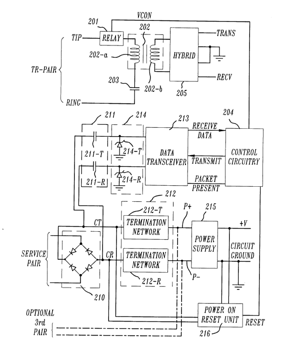
FIG. 2 is an exemplary imple~n~lion of apparatus required in a key
set to implement the in~.f~ce, including aspects of the invent on. The upper portion
of FIG. 2 displays the app~alus required for COI~ g to a TR-pair comprising
conduct~rs TIP and RING. Relay 201, I~;.f(.l~. 202 and non-polar cap ~itor 203
are con~,eh~d to the TR-pair, typically via a rm~ r telephone jack (not shown.)
25 ConJ~ TIP and RING carry at least loop current, voiceb~nA. c~nn~nic~tiQn and
an implem~nt~tion of tip and ring ringing signal (rin~ing signal) suitable for creating
an akr~ing inrlir,s~inn at a TR device. However, not all the abo~e-.~nl;~n~ signals
are car~ied ~imnllAncou~ly. The conneul;Qn of conductors TIP and R~NG may be
in~ hongPA without affecting circuit operation due to the sy~l~y of the circuit
30 and the signals passing through it.
The state of relay 201, which may be optical, is controlled by the value
of VCON. VCON is ~n~ ~d by control circuit 204. To this end, control circuit
204, by way of example, is l~is~n~, to rnPsesgPS received from key system
controller 101 (FIG.l), which is llltimstely l~s~onsihle for the value of VCON and
35 the c~ps>n~ling state of relay 201, as described below. Initially, VCON is set to a
first state which causes the circuit connp~tis~n though relay 201 to be open. The key
~04~022
- 4 -
set i~ thus effectively ~ conne~ted from the TR-pair. In acco -iancc with n aspect
of the invention, when the circuit c~nnPctiQn though relay 201 is open, loop current
will not be drawn nor will any ringing signal p~ss though the key set, i.e., loop
current and ringing signal are l~j~t~
In this example, voice access to the TR-pair by the key set is controlled
by signqling mPss-qges supplied over the service pair from key system controller 101
(FIG. 1). When appropriate signq-ling n~s~ges are received from key system
controller 101, e.g., in response to the ~1et~Pc~iQn of an off-hook con~lition at the key
set, control circuit 204 causes VCON to change state which, in turn, causes the
10 circuit conn~!;on though relay 201 to close. Nonnal operation requires that the
circuit conn~-!;on though relay 201 be closed only when the ringing signal has
ceased. However, in the event a ringing signal is applied while the circuit
conn~lion though relay 201 is closed, due to a fault condition, ringing signal will
pass through the circuit without affecting its operadon. Thus, ringing signal is15 ~ t~d by the key set interface, in accor~ance with an aspect of the invendon, since
the ringing signal is not altered in either state of relay 201. When relay 201 is
closed, a circuit path between TIP and RING is formed comprising relay 201,
ind~tnr 202-a, which is one half of transf~l 202, and c~--~ito 203. ~n~uct~r
202-a and c~parit~r 203 rapidly begin to charge with inductor 202-a eventually
20 becQming a direct current (DC) short circuit and c~p~citr~r 203 be~Q...ing a DC open
circuit In acco lance with an aspect of the invention, when fully charged, capaci~or
203 acting as an open circuit blocks the tran~mis~i~n of DC current thereby rejecting
loop current from the TR-pair during normal oper.ati~n
Altho~lgh DC loop current is blQcl~PA when relay 201 is closed,
25 voiceband signals pass freely through both in(l~ ~ 202-a and c~p ~ ~ 203. These
signal~ are ma~etic~lly coupled into ind~lct~r 202-b, the second h~f of transformer
202, in well Icnown faQhion r~lditionqlly~ voi~eb~nA signals appl~ed to inductQr202-b ~e m3~Ptirally coupled into inAuct~ 202-a and di~,." lially transmi~tPd
through relay 201 and cap ~itor 203 out onto the TR-pair.
Echoes on the cG.. -n~-ir~tion~ line should be minimi7PA to obtain good
quality voice c~.. ~nir~ion~ Therefore, the AC impeA~ r~ p.~i~nt~,d by in~luc~r
202-a, as seen by key system controller 101 (FIG. 1), should equal the imreA~nc~~-e~n~d by an ~ t~'A one of ports 103 (FIG. 1). Similarly, the AC impP~A~n~
p~5çnt~A by an ~SQci~tP~A~r one of ports 103 should match the AC impPAanr~
35 pnsenb~d by TR devices to be ~att~heA to the por~ It follows that the AC impeA~nre
of ind~letc~r 202-a, as seen by key system controller 101, should equal the im~nn~
Z0~5(~
of typ~l TR devices. In the United States this in~q~r is 600 ohms.
Voi~ebqnd signals to be tr~r~ ..;t~ from the key set are supplied as an
input to one port of hybrid 205 on the TRANS line. Voiceband signals received
from the key set are supplied as an output to another port of hybrid 205 on the RECV
5 line. The combined transmit and receive signals appear at the third port of hybrid
205 which, in this example, is connc~ed across inflllct~r 202-b. Hybrids, also
known as ~wire to 2-wire converters, are well known in the art.
The lower section of FIG. 2 shows exemplary apparatus for connecting a
key set to the se~vice pair of conductors. The service pair is compri~ of two
10 conductors CONTROL TIP (CT) and CONTROL RING (CR). Again, the service
pair carries at least bi-direction~l supervisory and control signals. In this example,
the service pair also ca ries operating power in-çn~ed for non-TR devices such as
key sets. In this example, CT is positive ~,vith respect to CR. The actual potential
dirr.,lence between CT and CR is at the imrlcn~ntor's discretion. For ease of
15 implem~nt-q-ti-n in a p.~ifell~d embcP~;nYnt CT is at ground p~t~ntiql and CR is at
approYim~t~ly -48 volts DC. Con~quçntly~ a single -48V DC power supply could
supply power both for key sets via the service pair and for TR devices via the TR-
pair. Bi di~ctionql diIT.,.~nlial data paclcets for transporting the supervisory and
control information are ~upe.;..~posed on the power carried on CT and CR. The data
20 p~L-çts~ in this example, are tr~n~mittçd in a ping-pong fq~hion Further, each data
paclcet comprises 24 bits, wherein the first 16 bits are the actual infw~llationcon~ ng a supervisory and control m~s~a~e and the last 8 bits are a checksum
co...pu~ in a pr~lll. ned fashion based upon the first 16 bits of infonmation.
Each 16 bit n~ssqg~ can yield only one ch~L`--." A data packet is valid when ~e 8
25 bit ck~L~ it c~-qinc c~l.,s~nd~ to the 16 bits of inf~m qti<~n therein. Each 16
bit p~n is ~ r~ as a commq-nl~ a status in~ic~q~ti~n or other n~c~ssq~y
inf~..~o~;~ l~ui~d to be transported ~I-.~n key system controller 101 and a key
set f ~.~p~ling imp~~mrntqtion of enhqnrcd funetiQnqlity fe~tulcs. In an example,
paclcet (XX)000000~10100010100 in~lir-q-t~s that a key set should sound a
30 pre~te....;l-~d alerting tone. The formation of such n~qge sets is well known in
the art. The data signals that are ~upelll~ d in this example co.lf~m to those
ii~lrse~ in United States Patent 4,454,383. Of course, utili7~n of any other
~ignqling n~thod that can be s.l~-,mposcd is not precludr,~1
Optional polarity guard 210, co~,~ing a diode bridge is qt-q-rh~d
35 direcdy to dle service pair. Polarity guard 210 insures that the signals fromconduct~r CI' actually are connectod to that part of the ;"~lf~qr~ expe~ting a more
'~0~''2
- 6-
~ potential. Further, polarity guard 210 insures that the signals fromcondu~ CR actually are CQn~Cl~,`ii to that part of the interface requiring a re
negative p~tenti~l Signals and power cxtracted from the more positive conductor by
polarity guard 210 are output at node CT. Signals and power extracted from the
S more negative cond~rtor by polarity guard 210 are output at node CR. Such
arPn~e..~nt~ are well known in the ar~
Node CT is connec~l to c~panit~r 211-T and te~nin~tion network 212-
T. Similarly, node CR is connpct~ to capacitor 211-R and terrnin~tion networlc
212-R. C`~p^^it~rs 211 block DC power from entering data transceiver 213 but
10 permit supervisory and control mpss~ges~ which are AC signals, to reach data
transceiver 213. Further, çapz~it~rs 211 receive supervisory and control ~ss~gesfmm data transceiver 213 and ~u~.~ )03e them onto the power present at
conductnrs CT and CR for tr~n~mi~siQn back through polarity guard 210 toward theservicc pair. ~d~ n~lly~ optional protection unit 214 protects data transceiver 213
15 from large voltage tr~n~;pnn that rnay bcco~c present on CT and CR. In this
eY~nple, protection unit 214 cornr~Ps zener diodes 214-T and 214-R configured toclamp any signal to their rated value.
When a pacl~et supplied from the service pair via ~p~~itors 211 is
~ ~r~,t~ by data t~neceiver 213, an inflir~tion is ~ P~ on the PACKET
20 PRESENT lead. In this example imp~ ,nl~lion, negative type logic is used for the
in~ple-r~ntor~s convçniPnre- Thus, the ~te~tion of the presence of a packet is
inAi~t~ by a logical 0 on thc PACKET PRESENT lead. Absencc of a packet is
inflir~tP~ by a logical 1 on the PACKET PRESENT lead. Message data 1PcQ~l~
from a paclcet i~ supplied as an output on the REOEI~E DATA lead to key set
25 cont~l ctrcuit 204. Data for tr~n~rni~ion from control circuit 204 to key system
con~oller 101 (FIG. 1) is sl~pplied as an input to data transceiver 213 on the
TRANSMIT lead~ Thc data is then dil`rtl~nlially ercod~ t~ansro.~L~d to
dy~,~iate signal levels and supplied as an output via capacitors 211 for
sU~ ;l;on onto conAalctors CT and CR. All~,...&li~ely, the di~ tial data
30 may be directly supplied over a pair of kads to data transceiver 213 or othern~Cc~r p~ce~;ng steps may be pe.rul~d by control circuit 204. As in~1ir~te~
above, any other ~ ng method may be used without departing from the spirit and
scope of the invention. If the service pair of c~ ~t~rs only carries supervisory and
control signals, polarity guard 210 and capacitors 211 are not need~ Data
35 I ~u~sceiver 213 would be connec~ directly to the service pair.
204~02~
-7 -
Terminq~ion networks 212 bloclc the transmi~sion of AC signals, i.e., the
data signals cQr~q;.~ g the control nd supervisory il~l..~tion, yet permit the
pqCQag! of DC signals, i.e., the opelaling power. In a p,~ .,d embodiment,
termin~ti.~n networks 212 are transistor based c~ns!~nt current drive~, which are
5 well ~nown. DC ope.aling power passes on leads P+ and P- to power supply 215
which provides regulated power at the voltage levels required for operation of the
circuitry in the key set. ~lternqttvely~ any terminqtion mq~rhing the re~lu~,l.ents of
the chosen transceiver circuit can be used. If a third cond-)ctQr pair or an alternative
source supplies opela~.ng power for the key set, optional polarity guard 210 . nd
10 terminqtion networks 212 are not requi~ TnQ~-~ the o~lating power supply
should connect directly or via a polarity guard to power supply 215 at leads P+ and
P-. Power on reset unit 216 genc~a~s a RESET in~lirqti~n that is supplied to control
circuit 204 for les~~ g and reinitiqli7ing the key set. A RESET in lirqtion is
supplied when the voltage supplied for p~ ,.ing a key set reaches a first
15 p~ t~,,n;necl value after having been less than a second pred~t4l~ned value which
is less than said first pl~tel.llined value. If operadng power is supplied on anopdonal third con~uctor pair, power on reset unit 216 would be connect~l cross
said third pair rather than across CI and CR
An alh~ a~ arrqn~m~nt for c~n~-l;ng to the TR-pair is shown in
20 FIG. 3. This arr-nge~nt achieves lower cost by elimin~q~ting the elcrnQ-ive relay
elen~n~ However, activation of the circuit for voice co~ n~ tion requires that asmall but fixed loop current be drawn from the TR-pair. In accordance with an
aspect of the invention, the amount of current drawn is ~ t~in~cl at a value smaller
than that which the chosen loop current ~ O~ in Icey system controller 101 (FIG.25 1) can detect and loop current beyond this ~l~.~l~led value is considered
~ t'YI An eyen~pl~ y current value is 7 mA. TL.~fol~" a ~ey set activated for
voice t~n~ni~Qion over an interfaced TR-pair will not g_n~..dt4 an off-hoolc signal to
key sy~em controller 101 at the termin~tir~n of the TR-pair on one of ports 103 (FIG.
1). An advantage derived from rejecting loop current so as not to g4AC~atc an off-
30 hoolc signal is that pulse (rotary) dialing from a TR device can be ~et~t~A at any ofports 103 even if the TR device is bridged onto said poqt in parallel with a Icey set.
Accordingly, con~uctora of the TR-pair from key system controller 101
are co--- e.~ to polarity guard 301 typically through a mod~ r telephone jack (not
shown). The main pul~oses and uses of polarity guard 301 are well known. When a
35 DC path is created ~I-._cn the conductors of the TR-pair, loop current is supplied as
an output from node TIP by polarity guard 301. Similarly, when the DC path is
- 8 -
crca~ed bct.~;n cQn~luct~ of the TR-pair, loop current is supplied as an input to
polarity guard 301 from RING.
VCON from control circuit 204 (FIG. 2) controls the comrletiQn of the
DC path between node TIP and node RING. When VCON is a logical 0 tn~nQi~t~r
5 302 is OFF, no current flows from node 303 and transistor 304 is c~l.,;.~n~linply
OFF. C~pacitQr 305 inhibits DC current from flowing through in~uct~r 30~a (one
half of transformer 306) resulting in polarity guard 301 being OFF, i.e., in a
nonr~n-lucting state. In accordance with an aspect of the invention, if a ringing
signal is received from Icey system controller 101 (FIG. 1) an initial conducting path
10 will ~.l~,~ily be set up through polarity guard 301, from llP to capacitor 305 and
in~luctor 306 a bacl~ through RING and polarity guard 301. During the first ringcycle, c~p ~ r 305 will quiclcly charge to the pealc value of the ringing signaLOnee charged, c~p~it~r 305 will bloclc any further tr~nQmiQQinn of ringing signaL
tiQnqlly, when the ringing signal is lc~.cd, the polarity of the charge on
15 ~ ~ci~r 305 reverses and thereby bac~ biases the diodes of polarity guard 301.
Cq~p~ o~ 305 will ll~.eÇolc be unable to discharge, except through resistor 307.The value of resistor 307 is chosen to provide a very large discharge time co~Qtqnt
relative to the interval of the ringing signal. This in effect rejects the ringing signaL
in ~ dance with an aspect of the invention. Diode 308 protects transistor 302
20 from ~lqmagç by the ringing signal that could be l,~n....;tb~A through capacitor 309.
When VCON is a logical 1 a current flows th~ough tr-qnsiot~r 302, diode
308 and resistor 312 activating a cono-~qn~ current source comprising tnq-no-iot~ 304,
resistors 313 and 314 and r~pr-itor 309. In turn, this causes a current to be drawn
from node TIP to node RING. The level of the cQnotqnt current drawn should be
25 s"~fi~ to allow the diodes that com~io~ polarity guard 301 to turn ON to transmit
vo ceband signals bi di~cti~nqlly without distortion. Al~ tive mechqnio-mo- for
p.~o.i.l;.lg the co~ current, such as opto-isolat~ can be used without violatingthe scope spirit of the invention. No AC signal flows Ih~OU~}I transistor 304. A
DC current also flows from node 310 through resistor 311 and in~t(~r 306 a to
30 RING.
The activation of the con~l~n~ current source creates an AC signal path
from node 310 to RING via resistor 312 and capacitor 309. An equal i...~Aince ACsignal path from node 310 to TIP com~rrio~ing resistor 311 and capacitor 305 insures
that any noise from node 310 is coupled equally to TIP and RING. I~e noise is thus
35 tr-q-ncmitt~ to the TR-pair through polarity guard 301 as inaudible c~---.~n mode
noise, rather than audible dirr~,~ntial noise.
Z04~0~
Whcn transistor 304 is ON, an AC cQn~Uct1ng path exists through
polarity guard 301, from TIP to c~pA^itor 30S and in~luct~r 306 a (one half of
~r 306) baclc thr~ugh RING and polarity guard 301. Voiceb~
co~ tiQn is inductively transferred from in~uct~-r 306 a to indllct~r 306 b and
S vic,e- versa in the same manner as for induct~rs 202-a, 202-b and hybrid 205 as
~Içscri~ for FIG. 2.