Note: Descriptions are shown in the official language in which they were submitted.
BURST AD ~ESS S~5~2UENOE3 GE~ATOR
~CRGROUND OF THIS INVE~TION
Generally, the pulse train burst addr~ss sequence
of a central processing unit (CPU) of the INTEL 80486 is
decided by the starting address; the customary technique
involves using the clock statle machine and basPd on the
value of the starting address to decide the sequence of
state transfer. To generate 2n pulse train addresses,
at least (2n)~1 states and n outputs are required. I~
the state machine is a progra~mable array logic (PAL) or
a programmable logic device (~PLD) to execute, then
(n~l)+n register outputs are required as (2n)~1 states
in a state machine and n register outputs for n bits of
pulse train addresses.
When n=2, four pulse train burst cycles should have
at least have 2~1+2=5 register outputs. Or, when n=3
(as in the case of write back cache o~ INTEL apogee
module), eight pulse train burst cycles can be made for
at least 3+1+3=7 register outputs. In this situation,
~0 generally there are only eight inputs used for the
device of the state machine (such as PAL or PLD with 20
or 24 pins); therefore, a single PAL or PLD can
accomplish th~ task.
When n=4 (at present, it is not available at
INTEL), however, based on design considerations of the
system, it is possible to divida a 128-bit pulse train
into two 64-bit pulse trains; thus, eight 128-bit pulse
train burst cycles will become 16 pulse train burst
cycles; then at least there should be 4~1+4=9 register
outputs. At that time, the design can only be completed
by adding 1 PAL or 1 PLD.
In conclusion, for each increm~nt o~ 1 in n,
requirements in register outputs should be incremented
by at least two registers. With this approach, the
following problems will exist: (1) the PAL or the PLD
should be increasPd ~or execution; (2) owing to the lack
224
of the expandable feature, the state machine should be
completely redesigned; (3) debugging should be
re-executed, among other problemsO
GENERAL DESCRIPTION OF ~HIS DNVENTION
This patent aims to provide a pulse train address
sequence generator which can be randomly expanded. The
generator has the following functions and effects.
1. This is low in price, composed of conventional
transistor-transistor logic (rrTL) elements.
2. The circuitry is simple and reliable.
3. Expansion can be randomly carried out to support 2n
pulse train sequences.
4. During expansion, no circuits may be changed by only
repeatedly using the id~ntical elements without
redesigning the circuit or debugging.
More particularly, this invention provides a pulse
train burst sequence generator to generate 2n pulse
train address sequences (n is an integer
greater than 1), including the following: one n-bit
binary up counter; the input terminal inputs signal
ZERO# of a burst pulse train address used to initialize
and to begin counting, and one increment signal IMC for
triggering the input: the output terminal is n count
signals C(0, ..., n-l) to couple and connect to an input
terminal of the n corresponding XOR gates (12); tha
starting addrass signal A(m, ..., m+n-l) (in other
words, the size of ea~h transmitted data of 2n pulse
train burst cycles is 2m bytes; Ao~ Am_l is the
continuous lowast address of these 2m bytes) being
coupled to another input terminal of the n
corresponding XOR gates in order tc obtain n pulse train
address signals SA(m, ..., m~n-1).
Additionally, this invention provides a pulse train
burst address sequence generator to generate 2n pulse
train address sequences ~n is an integer greater than
1~, including the following: one n-bit binary up
counter, whose input terminal inputs signal ZERO# of the
first pulse train address for initializing and to begi.n
counting, and an increment signal (INC) for triggering
the input; the output terminal of the binary up counter
bsing n count signals c(o~ ..., n-l) to couple and
connect to an input of the n-th corresponding XOR gate,
and a transparent latch, whosle input terminal inputs
one of n signals of the starting address bit A(m, ....
m+n-1) (that is, the size of leach transmitted data of 2n
pulse train burst cycles is 2~m bytes; Ao~Am_1 i5 the
continuous lowest address of this 2m bytes) and a
latched act signal (ALE); wherein, the output is the n
latched starting address signals LA(m, ..., m+n-1) and
hA(m, ..., m+n-1) to be coupled to another input
terminal of the n corresponding XOR gates in oxder to
obtain n pulse train address signals SA(m, ..., m~n-l).
Finally, this invention provides a pulse train
address sequence generator for reducing delay, including
one delay apparatus to be used to delay ~ t time of one
CAS# signal in input, ~t >tcah (tcah is the retaining
time of the column address a~ter the CAs# is low in
value);
one phase inverter, which is used to couple the
delayed CAS# signal to trigger input to a counter for
incrementing;
another input terminal of the counter which couples
and connects a signal ZERO# of the first pulse train
address generated for initializing and for counting to
begin; the output terminal being the n count signals
C(0, ..., n-l); and
n corresponding latched, multiplexing and XOR
gates, such that the input terminal of each one couples
and connects to a correspondins count signal C(0, ....
n-l), one corresponding address signal A(m, O~ m+n-l),
one corresponding row address (totalling n in number),
one multiplexing selection signal Mux, and one address
.
' -
.
.
.
4 ~5~
latched act tALE) signal to be used for the AL2 signal:when the signal is at the first value, the A(m, ....
m+n-l) address signal is latched into a latched signal
LA(m, ..., m+n-l) (totalling, there are n (0, l, ....
n-l) corresponding LA signals); when the ALE signal i~
at a second low value, then t:he A(m, ..., m+n+l) address
signal is transparent to signal MA(O, ..., n-l) (again,
there is a total of n(O, 1, ..., n-1) corresponding MA
signals); wherein when the fi:rst value is a high value,
the second value is low, and 1when the first value is a
low value, the second value is a high value.
&ENER~L DESCRIPTION OF TH~ DRAWINGS
One embodiment of this invention is illustrated in
the accompanying drawings, in which like numerals denote
like parts throughout the several views, and in which:
Figure l is a block diagram of the conventional
pulse train address sequence generating device;
Figure 2 is a schematic diagram for the address
bits in generating 2n pulse train addresses;
Figure 3 is a schematic diagram for gPnerally
produciny the sequence of the pulse train address
compatible with the CPU of the INTEL 80486 series;
Figure 4 is a schematic diagram for binary state of
the starting address based on the identified pulse train
sequence of this patent;
Figure 5 is a block diagram of the pulse train
address sequence generating device based on this patent;
Figure 6 is a block diagram explaining the
reduction in delay (based on this patent) of the pulse
train address sequence generating device; and
Fi~ure 7 is the timing diagram in coordination with
Figure 6 based on this patent.
DETAILED DESCRIPTION OF TH~ D~AWINGS
In the conventional pulse train address sequence
generating clevice (l), in Fig. l one first address
signal (such as column signal) Al is transmitted to a
timing state machine (3) after being latched with a
latch device (2) in order to follow a c2rtain sequence
to generate the required pulse train address ~ignal
(SA~. Capable of being used directly as the static
random access memory (SRAM), the address signal can also
be transmitted (along with one second address signal,
such as row signal) to a mult:iplexer (4) in order to
obtain an address signal (MA) of a dynamic random
access memory (DRAM). When t:he number n of the pulse
train address is incremented, the above-mentioned
problem will exist.
In the schematic diagram of the address bits as in
Fig. 2, 2m bytes are used as the fundamental
transmission unit of a circuit to generate 2n pulse
train burst cycles, the circuit should generate 2n pulse
train addresses; however, the form of the address bits
is shown in the figure. A0 and Al can possibly appear
in the form of BEO#-BE3#. In the case of the INTEL
80486 CPU, the fundamental unit in transmitting each
pulse train is 4 bytes (m=2); however, mostly four burst
cycles can be conducted. Therefore, the circuit should
generat~ two burst addresses of A2 and A3. In order to
generate pulse train address sequences compatible with
INTEL 80486 series CPU, the pulse train address A(m,
..., m+n-l) should follow the sequence determined by the
attached table in Fig. 3. ~ach pulse train sequence
should be decided only by the first address, that is,
the starting address. In the case of 486, the sequence
o~ ~our pulse trains is the same as the sequence in the
left upper corner and in the internal box.
In Fig. 4, the working principle of this patent is
based on the sequence in the attached table in Fig. 3.
By citing an example in which the starting address is
composed of four sets of pulse train address sequences
of 0, l, 2 and 3, the sequenca can be obtained by
rewriting in binary form. By carefully observing the
.
: ' ' ' - ' ,
.. : .. . .. : ' ' : .
.:, ' ', :'' , ', . ' . - ' , ~ , : ' ' ' ' . .
:: . - , , , . - .. . : :
. ,.: : --
,, .' '
binary form diagram, it can be discovered that the
binary sequence with the starting address as O is
actually an evolution of a binary up counting. On
viewing the other binary sequence, it can be discovered
that the i-th (i=o~ ..., n-l) bit of j (j=o, 1, ....
2n-1) pulse trains, and the i-th bit of binary value
with the j~th starting address as O should
simultaneously change the values (that is, O 1).
However, for each sequence,
for the value of bit 0/ thers is one phase reversal
for each increment in l in the count;
for the value of bit l, there is one phase reversal
for each increment in 2 in the count; and
for the value of bit n-1, there is one phase
reversal for each increment in 2n-1 in the count.
From this observation, one up counting of the
binary up counter can be used to tell at what time the
phase reversal should occur for various bits in a
sequence with a time base.
Aincrement, carafully observe Fig. 4; it can be
discoverad that besides the simultaneous state
conversion of the binary bit count for bit i in the
se~uence other than using O as the starting address, th
change into 1 or O should be det~rmined by the bit i of
the starting address.
If the value of the bit i of the starting address
is 1, then the value of bit i is just reversed to the
value of bit i in the converting and corresponding
binary counter in the j pulse train.
Conversely, i~ the value of the starting address
bit i is 0, then the value of bit i i~ the same as the
value of bit i in the oorresponding binary counter. In
other words, the values change simultaneously into 1 or
0. This means that the value of bit i in j pulse trains
(represented as Ai and j) and its relationship with an
XOR gate for bit i (expressed as Ci, j) of count j in
- .
. - ... : : . ' '
-
.. ',
.: , , ~, -.
d ;~ 4
the binary counter can be expressed as :+:. In other
words, Ai, j=Ci, ~ Ai,O.... Formula t~). In the
~ormula , Ai, O i5 the starting address.
sased on formula tl), tlle logic circuit shown in
5 Fig. 5 can be directly designed. Then
SA(m+j)=LA(m+j):+:C(j)... Fo~ula (2); in the formula,
j=O, ..., n-l; LA is the latched starting address A; SA
i5 the pulse train address. Formula (2) shows the
method of connecting the individual XOR in a particular
circuit. If 2n is required, there should be one n bit
binary up counter and n XOR gates.
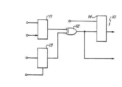
In Fig. 5, the pulse train burst address sequence
generator (10) is used to generate 2n pulse train
address sequences (n is an integer greater than or equal
to 1), including the following: one n-bit binary up
counter (ll), whose input t~rminal inputs increment
signal (INC) used for initializing and to begin counting
in order to generate a signal (ZERO#) of the first pulse
train address, and an increment signal (INC~ for
triggering the input. The output terminal is n count
signals C~O, l, ..., n-1) to couple and connect to the n
corresponding XOR gates (12); one transparent latch
(13), the input terminal inputs one of the n address
bits A(m, ..., m+n-l) signals (in other words, the size
of each transmitted data is 2m bytes for 2n pulse train
~urst cycles; Al~,AM-l is the continuous lowest address
of this 2m bytes) and one latched act signal (ALE).
However, the output is the n latched address signals
LA(m, ..., m~n-1), as well as n count signals C(O, l,
..., n-1) and n latched address signals L~ (m, ....
m+n-l) to be coupled to the n corresponding XO~ gates.
A(m, ..., m+n-l) is the starting address; after the
transparent latch locks A, A(m, ..., m+n-1) can be
randomly var:ied. If the starting address does not
change in the entire cycle of pulse train trans~ission,
this transparent latch (13) is not necessary, but can be
. . :' ' ' '
.
~0~5~
replaced with A(m, ..., m+n-1) for L~(m, ..., m~n-l) to
be directly coupled to the n th corresponding XOR gate
in order to obtain n pulse train address signals SA(m,
..0, m+n-l) to be directly coupled to a static random
access memory (SRAM) or a mu].tiplexer (14) to become an
address signal of the dynamic memory (DRAM).
Since the XOR gate and the multiplexer in Fig. 5
have two levels of delay, in order to reduce to one
delay level, a module of a dynamic random access memory
(DRAM) is used to change Fig. 5 into the circuit as in
~ig. 6.
As shown in Fig. 6, this is a pulsa train sequence
generating device (20) capable o~ reducing the delay in
generating the pulse train address, including the
following: one delay unit (21) to be used in delay time
~t for the CAS# (CAS~ is the signal of capturing the
column address for access of data of dynamic RAM);
however, ~t > tcah (tcah is the retaining time af~er
changing act at CAS# for the column address); one phase
inverter (22) to be used in phase reversal and coupling
the delay CAS# to a counter (23) to make an increment
for the counter; another input terminal of the counter
(23) couples for initializing and to begin counting in
order to generate a signal ALE of the first pulse train
address; the output terminal is n counting signals C(O,
1, ..., n-l). In addition, n corresponding lat~hing,
multiplexing and XOR gates (24) can be one PAL or one
PLD; each input terminal is coupled with a corresponding
counting cycle, a corresponding address signal A(m, ....
m+n-l), a corresponding row address RA(O, 1, ..., n-l),
and one multiplexer multiplexing selection signal Mux to
be used to select the address of the dynamic memory as
column or row address. In addition, there is an address
latched act signal (ALE), whose output is address MA(O,
..., n-l) of the dynamic memory; when the ALE is o~ high
value (or low value), the A address signal is locked
. ~ ' .
,.. ' ~ ' . .
,~ " ' ' . '
~0~5~
into a latched signal LA(totalling 0, 1, ..., n-l) in n
corresponding LA signals; however, when the LA signal is
a low value (or high value), the A address signal is
transparent to become MA signal (totalling n
corresponding signals (o, 1, ..., n-l). In the pulse
train address sequence generator (20), in addition to
executing the latch function :in the logic devicP PAL or
PLD, there should be functions of XOR gate and
multiplexer to be used in executing the function
corresponding to (13), (12) and (14) in Fig. 5. The
following are the computations:
MA(i)=Mux RA(i)+/Mux A(m~i) /AL~+/Mux [LA(m+l):+:C(i)-
]-ALE ~3)
In the formula, LA(m~i) is the latched address signal
A(m+i), and
RA(i) is the corresponding row address;
A(m+i) is the starting address.
"+" is OR logic,
" " is AND logic,
":+:" is XOR logic,
Mux is the multiplexing selection signal,
/ALE is the phase reverse ALE signal, and
/Mux is the phase reversed Mux.
The timing at the operation in Fig. 5 is shown in
Fig. 7. In Fig. 7, CS# (CYCLE ST~RT) is a transmitting
cycle start signal; when the signal is at a low value,
the starting address A will ~e transmitted. As CS#, ALE
becomes a low value at the same time. At this time, the
counter should reset to be initialized because each
pulse train transmission should begin from the starting
address from O relative to the C value. When ALE is
LOW, the counter is cleared. In addition, frsm formula
(3), we know if the Mux signal is a low value, MA is A.
In other words, at that time A is transparent to MA
because the MA generated time will not satisfy the
address acce~ss time (tAA) of SRAM if executing with the
. :
~o
direct logic of C:+:A=MA; the reason is that the time is
too long from ALE to clear C to zero in counting. For
each increment of the counter, based on formula (1) an
instruction is given to the XOR logic to generate a
pulse train address; however, the counter generates
increments (INC) as the increment trigger of the counter
with delayed CAS# before phase reversal. Thus, when
completing one transmission of pulse train data, the
CAS# completes a ~ycle from high value to low value and
increment returns to high value; the counter then
automatically has an increment of one.
--
.
-