Note: Descriptions are shown in the official language in which they were submitted.
2045330
FAST SETTLING, WIDE DYNAMIC
RANGE VECTOR MODULATOR
BACKGROUND OF THE INVENTION
Field Of The Invention
This invention generally relates to signal controllers, and more specifically relates
to a vector modulator which is suitable for use as an RF signal controller in aninterference cancellation system. Even more specifically, this invention relates to a
vector modulator particularly adapted for high speed, wide dynamic range applications.
Description Of The Prior Art
A vector modulator is sometimes referred to as a signal controller. It is a circuit
which primarily functions to adjust the amplitude and phase of a signal.
One of the primary applications of a vector modulator is in an interference
cancellation system, such as disclosed in U.S. Patent No. 3,699,444, which issued to
Rabindra Ghose et al. In such an interference cancellation system, the vector modulator
generally receives a sample of a transmitter signal, which may be causing interference in a
collocated receiver system, and adjusts the amplitude and phase of the sampled signal to
provide a cancellaton or correction signal which is essentially the negative complement of
the transmitter signal. The cancellation signal is injected into the signal path of the
receiver system to cancel or at least minimi7e the interference caused by the transmitter
slgnal.
Generally, the vector modulator works in conjunction with a synchronous or
coherent detector and a loop amplifier and filter. The detector compares a sample of the
received signal with that of the transmitter signal and provides control signals to the
vector modulator via the control loops that minimi7e the synchronous detection products of
the two sampled signals. The vector modulator adjusts the amplitude and phase of the
sampled transmitter signal in accordance with the control signals it receives from the
control loops.
More specifically, the vector modulator adjusts the amplitude of the in-phase
and quadrature phase, or sine and cosine, components of the reference or sampledtransmitter signal. By so doing, a cancellation signal may be provided with the desired
2045330
amplitude and phase angle. Accordingly, a typical vector modulator, such as disclosed in
the Ghose et al. patent, includes two signal controllers 39, 40, each for respectively
modifying the in-phase or sine component and the quadrature phase or cosine component
of the sampled signal.
An early form of a signal controller is disclosed in U.S. Patent No. 3,550,041,
which issued to Walter Sauter. Fig. 1 of this patent shows a signal controller having a
transformer 13 which basically provides two output signals corresponding to the input RF
signal, which output signals have a phase angle difference of l 80~. The secondary
winding of the transformer 13 is connected to two PIN diodes 20, 21. A DC bias signal
provided to each PIN diode allows one or the other of the output signals to be selected.
By adjusting the bias signals, attenuation of the selected signal may be controlled. In
effect, two such signal controllers would be required in forming a vector modulator,
each controller being employed to adjust in amplitude either the in-phase or the quadrature
phase component of the RF signal.
U.S. Patent No. 4,016,516, which issued to Walter Sauter, et al., discloses another
conventional vector modulator, which is referred to in the patent as a signal controller. As
shown in Fig. 3 of the Sauter, et al. patent, a quadrature hybrid 51 is used to produce the
in-phase and quadrature phase components of a reference signal, and an in-phase hybrid or
zero degree summer 60 is used to sum the components back together.
Each of the in-phase and quadrature phase components is adjusted in amplitude byusing a quadrature hybrid 55, 56 and a pair of PIN diodes 61, 62 and 63, 64, used as
terminations. The bias of the PIN diodes is controlled in a manner similar to that described
in U.S. Patent No. 3,550,041 to adjust the amount of the in-phase and quadrature phase
components which is absorbed by the PIN diodes and the amount which is reflectedthrough the quadrature hybrids 55, 56 and summed in the zero degree summer 60 toproduce a cancellation signal.
The signal controllers (or vector modulators) disclosed in U.S. Patent Nos.
3,550,041 and 4,016,516 work well in many applications. However, the application of
interference cancellation techniques to frequency agile and broad instantaneous
bandwidth systems requires increased vector modulator performance, and in such
applications, the signal controllers disclosed in the aforementioned patents may have
3 2045330
limited capabilities due primarily to the PIN diodes employed in the controllers, and
their associated insertion phase variation over the amplitude control range.
- Many conventional interference cancellation systems are of the fixed geometry,
fixed frequency type. That is, the geometry between the interfering signal source
and the receiver antenna is fixed, and also such interference cancellation systems
tend to operate with a very narrow bandwidth and at a particular frequency. Oncethe system is tuned up, there is relatively little change in the in-phase and quadrature phase
loops of the system that the vector modulator would experience.
However, in an interference cancellation system which must be able to respond tomany different frequencies and in which the antennas have a different response at such
frequencies, the in-phase and quadrature phase control values may change radically. The
vector modulator must be capable of responding quickly and accurately to such changes.
Thus, frequency agile systems require the vector modulator to respond
quickly after being commanded from a previous setting. PIN diodes have relatively
large parasitic capacitances, which tend to slow down the response time of the signal
controller or vector modulator employing the diodes, as it is difficult to move charge
quickly in and out of the diode's capacitance. Smaller geometry PIN diodes may be
employed in the vector modulator to improve response time, but not without a reduction in
power handling capability and a corresponding increase in the amplitude of distortion
products.
In many interference cancellation system applications, vector modulators must becapable of h~n~ling large input signal powers. To handle such large input powers,
conventional vector modulators would require large geometry PIN diodes. Larger
geometry PIN diodes correspondingly have greater parasitic capacitance, which tends to
slow down the response time of the vector modulator. Accordingly, there is a
speed/power tradeoff when using a PIN diode in a vector modulator.
Another problem with PIN diode type vector modulators is that the phase and
amplitude response of the vector modulator may vary with respect to frequency. PIN
diodes, especially those which are capable of handling larger power levels, are fairly large
devices. Many PIN diodes tend to be discrete components, as opposed to monolithically
formed chip type devices, and thus have lead inductances and parasitic capacitances
associated with them. Their intrinsic characteristics form resonant circuits, which may
2045330
cause the vector modulator to change in its response as a function of the frequency of the
signal it is handling. This affects the performance characteristics of the interference
cancellation system in which the vector modulator is used.
Similarly, the phase and amplitude response of conventional PIN diode
modulators may be affected by thermal drift in the PIN diodes. In conventional vector
modulators, the PIN diodes must absorb a sizeable portion of the signal power. The
diodes tend to heat up, which may cause their electrical characteristics, such as their RF
resistance, to change. As a result, the phase and amplitude correction the PIN diode
modulator imparts to the RF signal may differ from the correction expected from the
values applied to the bias or control ports of the vector modulator by the control loops.
Another problem with many conventional vector modulators used in interference
cancellation systems is that their insertion phase tends to vary as a function of the
attenuation they apply to the signal. If the insertion phase of each of the in-phase and
quadrature phase paths through the vector modulator is not independent of its attenuation
setting, the relationship between the in-phase and quadrature phase components will
deviate from 90~ after passing through the signal controller portions of the modulator.
Furthermore, each component will differ in phase from its counterpart in the synchronous
detector. Accordingly, a change in the in-phase component due to the insertion phase
shift will affect the quadrature phase component. The quadrature phase signal control
loop of the interference cancellation system will accordingly make a correction to
the quadrature phase component, and that correction will, in turn, impact the in-phase
signal control loop of the system. In other words, the two system control loops will no
longer be independent of each other. A change in the output of one control loop will
affect the other, and this will prolong the "settling time" of the entire cancellation system.
OBJECTS AND SUMMARY OF THE INVENTION
It is an object of the present invention to provide a vector modulator which is
particularly adapted for high speed, wide dynamic range applications.
It is another object of the present invention to provide a vector modulator having a
relatively short response time.
2045330
It is a further object of the present invention to provide a vector modulator
having an insertion phase which remains relatively constant over a relatively large
attenuation range.
It is yet a further object of the present invention to provide a vector modulator
which has a relatively flat phase and amplitude response over a relatively large frequency
range and is thus capable of broadband operation.
It is still another object of the present invention to provide a vector modulator
which is adapted for use in an interference cancellation system.
It is yet a further object of the present invention to provide a vector modulator
which overcomes the inherent disadvantages of known vector modulators.
A vector modulator formed in accordance with one form of the present invention
includes a quadrature hybrid. The quadrature hybrid receives an RF signal to be
adjusted, and provides a primary in-phase component and a primary quadrature phase
component signal corresponding to the RF signal.
A first 180~ hybrid is connected to one output port of the quadrature hybrid andreceives the primary in-phase component signal. The first 180~ hybrid provides first
and second secondary in-phase component signals, each corresponding to the primary in-
phase component signal. The first secondary in-phase component signal is 180~ out of
phase with the second secondary in-phase component signal.
A second 180~ hybrid is also included, and is connected to the other output port of
the quadrature hybrid and receives the primary quadrature phase component signal. The
second 180~ hybrid provides first and second secondary quadrature phase component
signals, each corresponding to the primary quadrature phase component signal. The first
secondary quadrature phase component signal is 180~ out of phase with the secondsecondary quadrature phase component signal.
The vector modulator also includes a first switching device for selecting one of the
first and second secondary in-phase component signals in response to a first control signal.
The first switching device provides a selected in-phase component signal
corresponding to one of the first and second secondary in-phase component signals.
A second switching device is also included and selects one of the first and
second secondary quadrature phase component signals in response to a second control
signal. The second switching device provides a selected quadrature phase component
6 2045330
slgnal corresponding to one of the first and second secondary quadrature phase component
slgnals.
The vector modulator further includes a first coarse attenuator. The first
coarse attenuator provides coarse attenuation to the selected in-phase component signal.
The first coarse attenuator receives the selected in-phase component signal and
attenuates the selected in-phase component signal by a predetermined amount in
accordance with a third control signal provided to it. The first coarse attenuator then
provides a coarse attenuated in-phase component signal.
The vector modulator also includes a second coarse attenuator for providing
coarse attenuation to the selected quadrature phase component signal. The secondcoarse attenuator receives the selected quadrature phase component signal and attenuates
the selected quadrature phase component signal by a predetermined amount in accordance
with a fourth control signal provided to it. The second coarse attenuator provides a
coarse attenuated quadrature phase component signal.
The vector modulator also includes first and second fine attenuators. The first
fine attenuator provides fine attenuation to the selected in-phase component signal. The
first fine attenuator receives the coarse attenuated in-phase component signal and attenuates
the coarse attenuated in-phase component signal by a predetermined amount in accordance
with a fifth control signal provided to it. The first fine attenuator provides a fine
attenuated in-phase component signal.
The second fine attenuator provides fine attenuation to the selected quadrature
phase component signal. The second fine attenuator receives the coarse attenuated
quadrature phase component signal and attenuates the coarse attenuated quadrature
phase component signal by a predetermined amount in accordance with a sixth control
signal provided to it. The second fine attenuator provides a fine attenuated quadrature
phase component signal.
The vector modulator further includes a signal combiner for combining the fine
attenuated in-phase and quadrature phase component signals. The signal combiner receives
and sums the fine attenuated in-phase component signal and the fine attenuated
quadrature phase component signal, and provides an adjusted signal which corresponds to
the vector sum of the two signals.
,~.
2045330
The vector modulator may also include a control interface device which provides
the first and second control signals to the first and second switching device, the third and
fourth control signals to the first and second coarse attenuator, and the fifth and sixth
control signals to the first and second fine attenuator.
These and other objects, features and advantages of this invention will be apparent
from the following detailed description of illustrative embodiments thereof, which is to be
read in connection with the accompanying drawings.
BRIEF DESCRIPTION OF THE DRAWINGS
Fig. 1 is a block diagram of a vector modulator formed in accordance with the
present invention.
Fig. 2 is a pictorial representation of the in-phase and quadrature phase
components, illustrating the effect of one component on the other due to attenuation
changes in the vector modulator.
DETAILED DESCRIPTION OF THE PREFERRED EMl~ODIMENTS
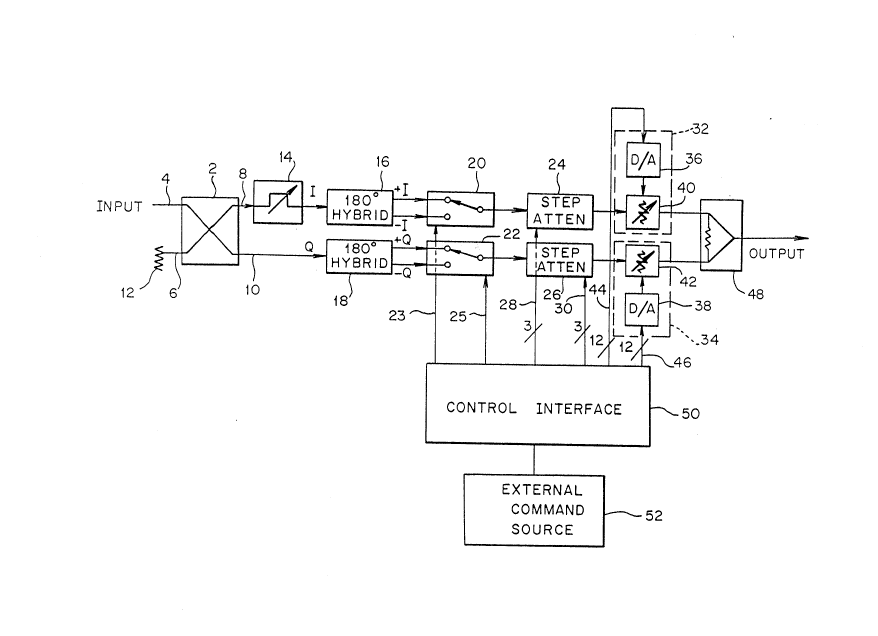
Referring initially to Fig. 1 of the drawings, it will be seen that a vector modulator,
constructed in accordance with one form of the present invention, includes a quadrature
hybrid 2 or similar device. The quadrature hybrid 2 includes two input ports 4, 6, and two
output ports 8, 10. One input port 4 receives an input RF signal which is to be adjusted in
phase and amplitude. The other input port 6 is termin~ted using an appropriate
termination 12. As its name implies, the quadrature hybrid 2 provides two output signals
which are 90~ out of phase with each other. The first output signal is termed a primary
in-phase component signal, and is provided on output port 8. The second output signal is
termed a primary quadrature phase component signal, and is provided on output port 10.
The primary in-phase component signal and the primary quadrature phase
component signal correspond to the RF signal provided on input port 4
The primary in-phase component signal provided on output port 8 of quadrature hybrid 2
is provided to a phase adjustment device 14. The phase adjustment device 14 may be in
the form of a variable delay line or the like. The purpose of the phase adjustment device
14 is for adjusting for any phase difference from the desired 90~ between the primary in-
phase component signal and the primary quadrature phase component signal. More
8 2045330
specifically, the phase adjustment device 14 is provided to adjust for cabling differences
and insertion phase differences between components in the in-phase and quadrature phase
~ paths of the vector modulator so that the two paths may be tuned to achieve a substantially
perfect 90~ balance between the primary in-phase component signal and the primary
quadrature phase component signal.
Although Fig. 1 illustrates the phase adjustment device as being connected to
output port 8 and being provided in the signal line carrying the primary in-phase
component signal, device 14 may have been connected to the output port 10 of quadrature
hybrid 2 to receive and adjust the primary quadrature phase component signal to
ensure that the primary in-phase and quadrature phase component signals are 90~ apart
from each other. Alternatively, two phase adjustment devices may be included in the
vector modulator, one in the signal line carrying the primary in-phase component signal to
adjust the primary in-phase component signal and the other in the signal line carrying the
primary quadrature phase component signal to adjust the primary quadrature phasecomponent signal.
As illustrated by Fig. 1, the primary in-phase component signal, which has passed
through phase adjustment device 14, is provided to a first 180~ hybrid 16. The first 180~
hybrid 16 is responsive to the primary in-phase component signal and includes two output
ports on which are respectively provided first and second secondary in-phase
component signals (designated in Fig. 1 as +I and -I). Each of the first and second
secondary in-phase component signals corresponds to the primary in-phase component
signal. As its name implies, the 180~ hybrid 16 provides a first secondary in-phase
component signal which is 180~ out of phase with the second secondary in-phase
component signal.
Similarly, the primary quadrature phase component signal on output port 10 of
quadrature hybrid 2 is provided to the input of a second 180~ hybrid 18. Like hybrid 16,
the 180~ hybrid 18 takes the primary quadrature phase component signal and resolves it
into two signals which are 180~ out of phase with respect to each other. More
specifically, the second 180~ hybrid 18 has two output ports on which are respectively
provided first and second secondary quadrature phase component signals (designated in
Fig. l by +Q and -Q) . Each of the first and second secondary quadrature phase
component signals corresponds to the primary quadrature phase component signal
X
9 2045330
provided to hybrid 18. The first secondary quadrature phase component signal is 180~ out
of phase with the second secondary quadrature phase component signal.
The vector modulator further includes two switching devices 20, 22. Each
switching device 20, 22 is schematically illustrated in Fig. 1 as a single pole, double throw
switch, and effectively operates in that manner. Devices 20, 22 may be GaAs FET RF
switches, PIN diode RF switches, or the like.
The first switching device 20 is provided for selecting one of the first and
second secondary in-phase component signals, and receives these signals from the output
ports of the 180~ hybrid 16. The first switching device 20 selects either secondary in-
phase component signal in response to a first control signal provided to it, and provides on
its output a selected in-phase component signal corresponding to one of the secondary in-
phase component signals.
The second switching device 22 similarly selects one of the first and second
secondary quadrature phase component signals in response to a second control signal
provided to it. Switching device 22 receives the first and second secondary quadrature
phase component signals from 180~ hybrid 18, and provides a selected quadrature phase
component signal on its output which corresponds to one of the secondary quadrature
phase component signals.
A suitable RF switch which may be used for the first and second switching
devices 20, 22 is model no. SW-215 manufactured by Anzac, a division of Adam-
Russell Co., Inc. of Burlington, Massachusetts. Switching devices 20, 22 may be
digitally controlled such that the first and second control signals are single bit digital
words provided to the switching devices on data lines 23, 25, respectively.
The selected in-phase component signal from the first switching device 20 is
provided to a first coarse attenuator 24. The first coarse attenuator 24 provides coarse
attenuation to the selected in-phase component signal. The first coarse attenuator 24
attenuates the selected in-phase component signal by a predetermined amount in
accordance with a third control signal provided to it, and provides on its output a coarse
attenuated in-phase component signal.
Similarly, the selected quadrature phase component signal from the second
switching device 22 is provided to a second coarse attenuator 26. Second coarse
attenuator 26 provides coarse attenuation to the selected quadrature phase component
~.
2045330
signal. The second coarse attenuator 26 attenuates the selected quadrature phasecomponent signal by a predetermined amount in accordance with a fourth control signal
provided to it, and provides on its output a coarse attenuated quadrature phase component
slgnal.
The first and second coarse attenuators 24, 26 may be in the form of step
attenuators, each of which is comprised of selectively switched attenuation pads. The step
attenuators are digitally controlled to add or remove a predetermined amount of
attenuation to the selected in-phase and quadrature phase component signals provided to
the coarse attenuators. Each of the third and fourth control signals is in tile form of three
bit digital data and is respectively provided to its corresponding coarse attenuator on a
three bit data bus 28, 30. A suitable step attenuator for use as the first and second coarse
attenuator 24, 26 is model no. DAO-041 manufactured by Anghel Labs, Inc. of
Rockaway, New Jersey, or one of the MA4GM400 series of attenuators manufactured by
M/A-Com, Inc. of Burlington, Massachusetts. The first and second coarse attenuators
24, 26 respectively provide on their outputs a coarse attenuated in-phase component
signal and a coarse attenuated quadrature phase component signal.
The coarse attenuated in-phase component signal *om the first coarse attenuator
24 is provided to a first fine attenuator 32. The first fine attenuator provides fine
attenuation to the selected in-phase component signal. The first fine attenuator 32
attenuates the coarse attenuated in-phase component signal by a predetermined amount in
accordance with a fifth control signal provided to the first fine attenuator 32, and
provides a fine attenuated in-phase component signal on its output.
Similarly, the coarse attenuated quadrature phase component signal from the
second coarse attenuator 26 is provided to a second fine attenuator 34. The second
fine attenuator 34 provides fine attenuation to the selected quadrature phase
component signal. The second fine attenuator 34 attenuates the coarse attenuatedquadrature phase component signal by a predetermined amount in accordance with a sixth
control signal provided to the second fine attenuator 34, and provides a fine attenuated
quatrature phase component signal on its output.
Each of the first and second fine attenuators 32, 34 has a usable attenuation range
which is respectively greater than the predetermined amount of attenuation provided by
11 2045330
each coarse attenuator 24, 26 by a predetermined amount of attenuation, as will be
explained.
Preferably, each of the first and second fine attenuators 32, 34 is digitally
controlled and includes a digital-to-analog converter 36, 38 whose analog output is
provided to a variable (i.e., analog) attenuator 40, 42. Variable attenuators 40, 42 are
preferably microwave monolithic integrated circuit (MMIC) devices, such as model no.
MA4GM301L manufactured by M/A-Com, Inc.
For greater resolution, the digital-to-analog converters 36, 38 used in the first and
second fine attenuators 32, 34 are preferably 12 bit devices and, accordingly, the fifth and
sixth control signals provided to the digital-to-analog converters are 12 bit digital words
provided on 12 bit data bus lines 44, 46, respectively.
The fine attenuated in-phase component signal from the first fine attenuator 32, and
the fine attenuated quadrature phase component signal from the second fine attenuator 34
are provided to a signal combiner 48. The signal combiner sums the fine attenuated in-
phase and quadrature phase component signals and provides an adjusted signal on its
output which corresponds to the vector sum of the two. By selecting one of the first and
second secondary in-phase component signals (+I and -I) and one of the first and second
secondary quadrature phase component signals (+Q and -Q), and by providing a
predetermined amount of attenuation to each of these selected signals, the vector
modulator of the present invention provides an adjusted output signal having thedesired phase and amplitude. When used in an interference cancellation system, the
correction or adjusted signal produced by the vector modulator may be used to
cancel an interfering signal in a receiver system to which the interference cancellation
system is coupled. The vector modulator of the present invention may further include a
control interface circuit 50. The control interface circuit may be in the form of a serial to
parallel converter and transparent latching circuit, and provides the first and second
control signals to the first and second switching devices 20, 22 in order to select one
of each of the first and second secondary in-phase component signals and first and
second secondary quadrature phase component signals, the third and fourth control
signals to the first and second coarse attenuators 24, 26, and the fifth and sixth control
signals to the first and second fine attenuators 32, 34. The control interface circuit 50
essentially decodes and distributes to the vector modulator elements command data
2045330
12
provided to it from an external source 52, for example, the control loops of an
interference cancellation system.
As mentioned previously, each of the first and second fine attenuators 32, 34 has a usable
attenuation range which is respectively greater than the predetermined amount ofattenuation of each step of attenuation provided by each of the first and second coarse
attenuators 24, 26.
For example, each step of the coarse attenuators 24, 26 preferably provides 8 dB of
attenuation. The fine attenuators 32, 34 are preferably selected to provide 10 dB of
attenuation over their entire range, thus providing a 2 dB overlap. This overlap in
attenuation between the fine attenuators and the coarse attenuators provides a certain
amount of hysteresis to avoid an oscillatory condition and to minimi~P the settling time of
the system in which the vector modulator is used. The reason for the attenuation overlap
between the fine and coarse attenuators and the method used to calculate the approximate
amount of hysteresis needed are described below with reference to Fig. 2.
Without some overlap of the coarse attenuator step boundaries by the fine
attenuator, phase discontinuities at a coarse attenuator step boundary may cause a lack of
convergence to the desired output vector. If, for example, a step change in one of the
coarse attenuators 24, 26 causes a 2~ phase shift in the in-phase path of the vector
modulator and, a corresponding full range change in the fine attenuator 32, 34 of the
same path as it is reset to the other end of its range causes a 5~ phase shift in the in-phase
path, the combined phase shift causes a change in the amplitude of the quadrature phase
component at the output of the vector modulator, since the in-phase path is now
contributing to the quadrature component of the vector modulator output. This
resultant change in the amplitude of the quadrature phase component requires an
adjustment of the coarse or fine attenuators in the quadrature phase path of the vector
modulator. An adjustment of the attenuators in the quadrature phase path of the vector
modulator may, in turn, result in a phase shift in the quadrature phase path andaffect the amplitude of the in-phase component, requiring an additional change in
attenuators of the in-phase path of the vector modulator.
The worst case appears to occur when the in-phase component signals and
the quadrature phase component signals at the attenuators of the vector modulator
have the same amplitude, and both the in-phase and quadrature phase coarse attenuators
.
13 2045330
24, 26 are near step boundaries. Accordingly, a sufficient amount of overlap in
attenuation between the fine attenuators and the coarse attenuators is provided to elimin~te
the chance of the coarse attenuators oscillating back and forth across step boundaries,
causing lack of vector modulator convergence to the desired output vector.
The amount of attenuation overlap between the fine attenuators and the coarse
attenuators is a function of the maximum change in the quadratured component.
As shown in Fig. 2, if the in-phase component I crosses a step boundary of the
coarse attenuator, it causes a relatively small change in the in-phase component but a
relatively larger change in the quadrature component Q. A change in the
quadrature component is given by the trigonometric equation ~ Q = R sin (~), where R
represents the magnitude of the in-phase component, and ~ represents the total possible
phase shift due to the combined changes in the coarse attenuator and the fine attenuator.
If, as assumed previously, a step attenuation change in the coarse attenuator causes
a 2~ phase shift, and a range change in the fine attenuator causes a 5~ phase shift in the
in-phase path of the vector modulator, the total phase shift for the in-phase path is 7~
Accordingly, ~ Q = R sin 7~ which equals .122R, which approximately equals a 1.1 dB
change. For this reason, a 2 dB overlap in attenuation is preferably chosen. Thus,
any insertion change due to crossing a coarse attenuator boundary in one path through the
vector modulator will only cause the system to readjust the fine attenuator of the
quadrature phase path -- the coarse attenuator of the quadrature phase path would not
need to be adjusted, as the maximum adjustment needed would be within the 2 dB
extended range of the fine attenuator.
There are a number of advantages to providing a coarse attenuator 24, 26 and a
fine attenuator 32, 34 for each path of the vector modulator. Because of ch~nging
parasitic capacitance, each fine attenuator will exhibit a greater phase shift over its
attenuation range than the coarse attenuators. Furthermore, the magnitude of this
insertion phase change increases as the attenuation range of this continuously
variable attenuator is increased. However, this vector modulator preferably employs a
GaAs MMIC attenuator having less insertion phase change than its PIN diode counterparts,
and the arrangement of the coarse and fine attenuators described previously minimi7es
the range of use of each tine attenuator, which in turn minimi7~s the unintentional phase
shifts in the vector modulator.
14 2045330
The coarse attenuators 24, 26 on the other hand are preferably composed of
passive resistive elements which are selectively switched in and out of the in-phase and
quadrature phase paths, enabling the coarse attenuator to cause relatively inconsequential
phase shifts in the vector modulator over a much greater dynamic range of operation
than the fine attenuator.
Additionally, the advantage of using a coarse attenuator having a series of
selectable passive elements is that the insertion phase over the full dynamic range of the
coarse attenuator is substantially the same. For a three bit, 8 dB/step coarse attenuator, a
56 dB range in attenuation may be provided. Eight different attenuation values may be
selected without substantially ch~nging the insertion phase.
The vector modulator of the present invention is particularly adapted to
frequency agile, wide dynamic range interference cancellation system applications for
three basic reasons. First, the fast settling time of the GaAs MMIC fine and coarse
attenuators provides improved command response time compared with PIN attenuatorimplementations of the prior art at the same power handling capacity. Second, the
constant phase nature of this vector modulator over wide dynamic range compared with
conventional vector modulators allows one to decouple the in-phase and quadrature
phase loops of the interference cancellation system to keep the two loops
independent, thereby decreasing the system tracking and settling time. Third, the
vector modulator would also allow an interference cancellation system to handle
interference signals over a wide frequency range, as the attenuators of this vector
modulator are broader band in their frequency response than those of the prior art,
improving the usable bandwidth of the vector modulator.
Although illustrative embodiments of the present invention have been described
herein with reference to the accompanying drawings, it is to be understood that the
invention is not limited to those precise embodiments, and that various other changes and
modifications may be effected therein by one skilled in the art without departing from the
scope or spirit of the invention.
'~