Note: Descriptions are shown in the official language in which they were submitted.
204s360
TITLE OF THE INVENTION
Signal Detecting Device
BACKGROUND OF THE INVENTION
Field of the Invention
The present invention relates to signal detecting
devices, and more particularly, to a device employed in a
communication apparatus comprising automatically dialling
transmitting function for detecting a identification signal
which is a composite wave of a plurality of frequencies
transmitted from an exchange system via a telephone line.
BRIEF DESCRIPTION OF THE DRAWINGS
Fig. 1 is a block diagram of a structure of an
embodiment of the present invention.
Fig. 2 is a waveform chart indicating the
input/output signal of a voltage comparator in the
embodiment of Fig. 1.
Fig. 3 is a block diagram showing a structure of
a second embodiment of the present invention.
Fig. 4 is a circuit diagram specifically showing
the structure of a reference voltage generator of the
embodiment of Fig. 3.
Fig. 5 is a block diagram showing a structure of
a third embodiment of the present invention.
Fig. 6 is a waveform chart indicating the
input/output signal of a voltage comparator of the
embodiment of Fig. 5.
Fig. 7 is a block diagram showing a structure of
a conventional signal detecting device.
Fig. 8 is a characteristic diagram indicating the
input/output characteristic of a tone detector in~ the
conventional signal detecting device of Fig. 7.
2045360
Description of the Background Art
Many communication apparatus connected to a
public telephone line such as a facsimile apparatus are
provided with automatically dialling transmitting function.
Regarding the procedure of connection with a called device
by the automatically dialling transmitting function, a
communication apparatus receives a identification signal
transmitted from an exchange of a public telephone line or
a private branch exchange (a PBX, referred to as "exchange
system" hereinafter), to send a dial signal after making
determination that the exchange system is at a state that
can receive a dial signal.
The above-mentioned identification signal
comprises the so-called dial tone and busy tone. A
composite signal
~ 2
2045360
which is the composition of two different constant
frequency signals is generally used as an identification
signal.
A conventional signal detecting device for detecting
this composite signal is shown in Fig. 7.
The signal detecting device of Fig. 7 is implemented
to detect a composite signal that is a composition of a
signal of frequency f~ and a signal of frequency f2. The
signal detecting device comprises a CML (Connect Model to
Line) relay 1, a matching transformer 2, a modem 3, an
amplifier 4, tone detectors S and 6, and an AND gate 7.
CML relay 1 is a switching circuit for selectively
connecting the telephone line to either of matching
transformer 2 or amplifier 4. Matching transformer 2 is
inserted between CML relay 1 and modem 3 for matching the
characteristic impedance of the telephone line, and for
insulating modem 3 from the telephone line. Amplifier 4
amplifies the signal transmitted from the exchange system
in the automatically dialling transmission. Tone detector
5 detects the signal component of frequency fl from the
output of amplifier 4. Tone detector 6 detects the signal
component of frequency f2 from the output of amplifier 4.
AND gate 7 performs an operation of the logical product of
the outputs of tone detectors 5 and 6.
As shown in Fig. 8, tone detectors 5 and 6 provide a
~ 3
2045360
logic 0 signal when a frequency component within a range
(fo+~ f) centered about the frequency (fO) to be detected
is applied, and a logic l signal when a frequency
component outside the above mentioned range is applied.
When the outputs of tone detectors 5 and 6 are ~oth
logical 0, a composite signal comprising the frequency
components of fl and f2 from a telephone line is received
by the device. At this time, AND gate 7 provides a logic
0 signal.
The output of AND gate 7 is applied as a control
signal of an automatically dialling transmitting device
(not shown). The automatically dialling transmitting
device receives the logic 0 signal from AND gate 7 to make
determination that the exchange system is at a state that
can receive a dial signal. Then, a dial signal is
transmitted.
The above described conventional signal detecting
device had a disadvantage that the circuit structure is
complicated since two tone detectors having complex
structures are used. If the exchange system transmits a
signal of another frequency of f3 as another identification
signal in addition to the above described composite
signal, another tone detector must be provided for
detecting frequency f3 to result in a further complicated
circuit. The structure of the tone detector is disclosed
2045360
in, for example, Japanese Patent Laying-Open No.48-93203,
No. 48-93204, and No.48-93205.
SUM~ARY OF THE INVENTION
An object of the present invention is to provide a
signal detecting device that can detect a identification
signal with a simple circuit.
The signal detecting device of the present invention
is a device employed in a communication apparatus
comprising automatically dialling transmitting function
for detecting a identification signal that is a composite
wave of a plurality of frequency signals sent from an
exchange system via a telephone line. The signal
detecting device includes comparing means, counting means,
and determining means. The comparing means compares the
level of the signal transmitted through a telephone line
with a predetermined threshold value. The counting means
counts the number of pulses in the output signal of the
comparing means for a predetermined constant time period.
The determining means makes determination that the signal
transmitted through the telephone line is an
identification signal when the count value of the counting
means is within a predetermined given range.
In accordance with the present invention, a
identification signal can be detected with comparing
means, counting mean, and determining means that can be
2045360
implemented with a simple structure, without using a tone
detector having a complicated circuit structure, to obtain
a simple and economical signal detecting device.
The foregoing and other objects, features,
aspects and advantages of the present invention will become
more apparent from the following detailed description of
the present invention when taken in conjunction with the
accompanying drawings.
DESCRIPTION OF THE PREFERRED EMBODIMENTS
Embodiments of the present invention will be
explained hereinafter with reference to the drawings.
Fig. 1 is a block diagram of a structure of the
first embodiment of the present invention. Referring to
Fig. 1, the structures of CML relay 1, matching transformer
2, modem 3, amplifier 4 are similar to those of the
conventional signal detecting device of Fig. 7, and their
descriptions will not be repeated.
An automatic gain control circuit (AGC) is
provided between the input end and output end of amplifier
4 in the embodiment of Fig. 1. Furthermore, voltage
comparators 12 and 13, frequency counters 14 and 15, and a
determining circuit 16 are provided in the embodiment of
Fig. 1 instead of the tone detectors 5 and 6 and AND gate
7 in the conventional signal detecting device of Fig. 7.
The output signal of amplifier 4 is applied to each one
input end of voltage comparators 12 and 13. A first
reference voltage Vref1 is applied to the other input end of
voltage comparator 12 as the threshold value for comparison
(level discrimination). A second reference voltage Vref2 is
-
204536~
applied to the other input end of voltage comparator 13 as
a threshold value for comparison (level discrimination).
Frequency counter 14 counts the number of pulses included
in the output signal of voltage comparator 12 for a
constant time period. Frequency counter 15 counts the
number of pulses included in the output signal of voltage
comparator 13 for a constant time period. Determining
circuit 16 makes determination whether an identification
signal is transmitted or not from a telephone line
according to the output signals of frequency counters 14
and 15.
The operation and function of the embodiment of Fig.
1 will be explained hereinafter.
The signal sent from an exchange system via a
telephone line varies in signal level according to the
distance from the exchange system and the state of the
telephone line. It is desirable that the magnitude of the
above mentioned signal has no fluctuation in the
comparison (level discrimination) of the above mentioned
signal with a reference voltage in voltage comparators 12
and 13. AGC 11 makes constant the magnitude of the output
signal of amplifier 4 by controlling the amplification
factor of amplifier 4 according to the DC voltage of the
input signal for example.
Fig. 2 (a) shows a waveform of a identification
2045360
signal that is a composite wave of frequencies of fl and f2
transmitted from the exchange system, amplified by
amplifier 4. The waveform of Fig. 2 (a) indicates the
case of where fl = 440Hz, f2 = 330Hz, as an example.
Voltage comparators 12 and 13 compare the output voltage v
of amplifier 4 with the respective reference voltages Vref
and Vref2 to provide a logic 1 signal when the output
voltage V is larger than reference voltages Vref~ and
Vref2. The output signals of voltage comparators 12 and 13
are shown in Figs. 2 (b) and (c), respectively. Frequency
counters 14 and 15 receive the output signals of voltage
comparators 12 and 13, shown in Figs. 2 (b) and (c),
respectively, to count the number of pulses thereof for a
constant time period. The counted result output from
frequency counters 14 and 15 are applied to determining
circuit 16. Determining circuit 16 makes determination
whether the input signal from the telephone line is a
predetermined identification signal or not according to
the outputs of frequency counters 14 and 15.
That is to say, since each of fl and f2 that is the
frequency components of the identification signal has
constant frequency and a constant amplitude, the waveform
of the identification signal of Fig. 2 (a) attains a
constant waveform. If appropriate constant voltages are
applied as reference voltages Vrefl and Vref2 f voltage
2045360
comparators 12 and 13, the number of pulses counted by
frequency counters 14 and 15 will be a constant and
specific number. Assuming that the number value counted
by frequency counters 14 and 15 are Pcl and Pc2,
respectively, and the above mentioned specific number
value Scl and Sc2, respectively, Pcl = Scl and Pc2 = Sc2 when
the input signal from the telephone line is a
predetermined identification signal. By carrying out the
determination of this condition with determining circuit
16, an identification signal can be detected. However,
this is the ideal case. In practice, there may be some
error in fl and f 2 Of the identification signal transmitted
from the exchange system. Pcl and Pc2 fLuctuate within a
certain range due to noise of the telephone line or noise
within the signal detecting device of Fig. 1. Taking into
consideration the above mentioned fluctuating range + a,
determining circuit 16 is implemented to make
determination that a predetermined identification signal
is received when
(Scl - a) < PCl < (Scl + a)
and
(Sc2 - a) < Pcz ~ (Sc2 + a)
This allows practical detection.
Because the voltage comparator, the frequency
counter, and the determining circuit have a simple
-- 2045360
structure circuit in the embodiment of Fig. 1 instead of a
tone detector of a complicated structure, the entire
structure of the device is simplified in comparison with a
conventional signal detecting circuit shown in Fig. 7.
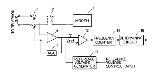
Fig. 3 is a block diagram of a structure of a second
embodiment of the present invention. Referring to Fig. 3,
voltage comparators 13 and frequency counter 15 in the
embodiment of Fig. 1 are removed, and one voltage
comparator 12 and one frequency counter 14 are provided.
Voltage comparator 12 is applied with reference voltage
Vref from a reference voltage generator 17. The output of
frequency counter 14 is provided to a determining circuit
18. The remaining structures of the embodiment of Fig. 3
is similar to those of Fig. 1. Therefore, equivalent
components have identical reference numbers denoted, and
their descriptions will not be repeated.
The signal detecting apparatus of Fig. 1 carries out
in parallel the comparison of two reference voltages Vref
and Vref2 and the counting of the pulse numbers thereof.
The signal detecting device of the embodiment of Fig. 3
carries out the comparison of two reference voltages Vref~
and Vref2 and the counting of the pulse numbers thereof in
time series. More specifically, reference voltage
generator 17 generates reference voltage Vrefl when applied
with a reference voltage control input of logic 1.
--10--
204~360
Reference voltage Vrefl is applied to voltage comparator
12, whereby voltage comparator 12 provides a pulse train
shown in Fig. 2 (b). The number of pulses included in the
output of voltage comparator 12 is counted for a constant
time period by frequency counter 14. The result output
Pcl counted by frequency counter 14 is applied to
determining circuit 18. When a reference voltage control
input of logic 0 is applied to reference voltage generator
17, reference voltage generator 17 generates reference
voltage Vref 2 which is applied to voltage comparator 12.
Voltage comparator 12 provides a pulse train shown in Fig.
2 (c). The number of pulses included in the output of
voltage comparator 12 is counted for a constant time
period by frequency counter 14. This result output Pc2
counted by frequency counter 14 is applied to determining
circuit 18.
Similar to determining circuit 16 of Fig. 1,
determining circuit 18 makes determination that a
predetermined identification signal is received when
(Scl - a) < Pcl < (Scl + a)
and
(Sc2 - a) < Pc2 < (Sc2 + a)
The embodiment of Fig. 3 has the circuit structure
further simplified than that of Fig. 1 since voltage
comparator 13 and frequency counter 15 shown in Fig. 1 are
--11--
- 2045360
removed.
Fig. 4 is a circuit diagram of an example of a
structure of reference voltage generator 17 of Fig. 3.
Referring to Fig. 4, reference voltage generator 17
comprises resistors Rl-R3 and a transistor TR. Resistors
Rl and R2 are connected in series between supply voltage
vcc and ground. Resistor R3 is connected between the
connection point of resistors Rl and R2 and the collector
of transistor TR. Transistor TR has the emitter grounded
and the base supplied with reference voltage control
input. Reference voltage Vref is obtained from the
connection point of resistors Rl and R2.
In reference voltage generator 17 of Fig. 4, when
reference voltage control input is logic 1, transistor TR
lS is turned on, and reference voltage Vref is:
R2//R3
Vref = Vcc = Vref
Rl+ R2//R3
where R2//R3 is the parallel resistance value.
When reference voltage control input is logic 0,
transistor TR is cut off, and reference voltage Vref is:
R2
Vref = Vcc = Vref 2
Rl+R2
If power supply voltage Vcc is a constant voltage,
reference voltage generator 17 can generate constant
-12-
- 2045360
reference voltages of Vrefl and Vref2.
The signal detecting device of Fig. 3 has a further
simplified circuit structure since the number of voltage
comparators and frequency counters can be reduced in
comparison with the numbers of the embodiment of Fig. 1.
Fig. 5 is a block diagram of a structure of a third
embodiment of the present invention. Referring to Fig. 5,
AGC 11 is not provided in amplifier 4 in this embodiment.
Therefore, amplifier 4 directly amplifies the input signal
from the telephone line to provide a signal according to
the input signal level to voltage comparator 12. Voltage
comparator 12 compares the level of the output voltage V
of amplifier 4 with a constant reference voltage Vref.
Frequency counter 14 counts the number of pulses of the
pulse train provided from voltage comparator 12 for a
predetermined time period. A determining circuit 19 makes
determination whether a predetermined identification
signal is received or not by carrying out the following
determination according to the count result output of
frequency counter 14. The remaining structure of Fig. 5
is similar to those of the embodiments of Figs. 1 and 3.
Because reference voltage Vref applied to voltage
comparator 12 is always constant, the number of pulses
included in the pulse train provided from voltage
comparator 12 varies according to the magnitude of the
-13-
2045360
identification signal provided from the telephone line, as
shown in Fig. 6. When the magnitude of the identification
~- signal is large as shown in Fig. 6 (a), the number of
pulses is increased. When the magnitude of the
identification signal is small as shown in Fig. 6 (c), the
number of pulses is reduced. However, the frequency
change is always constant even if there is fluctuation in
the magnitude of the identification signal since the
identification signal is a composite wave of constant
frequency signals. By setting in advance the maximum
value and the minimum value of the pulse number of a
constant time period obtained on comparing the level with
- a constant reference voltage Vref, the entry of an
identification signal can be detected within a practical
range, even if the magnitude of the identification signal
changes. Assuming that the maximum value is Scmax and the
minimum value is Scmin, determining circuit 19 makes
determination that a predetermined identification signal
is received if the pulse number Pc counted by frequency
counter 14 is Scmin _ Pc _ Scmax.
The embodiment of Fig. 5 has a further simplified
circuit structure than that of the embodiment of Fig. 3
because reference voltage generator 17 generating two
types of reference voltages is not required.
Although the above described embodiments are
-14-
2045360
implemented to detect an identification signal which is a
composition of two different frequencies, the invention is
not limited to the described embodiments, and an
identification signal which is a composition of three or
more types of frequencies can be detected. In this case,
the number of voltage comparators and frequency counters
should be increased according to the number of frequency
signals used for the composition of the identification
signal in the embodiment of Fig. 1. In the embodiment of
Fig. 3, the number of types of reference voltages
generated by reference voltage generator 17 should be
increased according to the number of the above mentioned
frequency signals. Because the embodiment of Fig. 5
always uses a constant voltage reference, detection of
reception of an identification signal can be carried out
directly with the structure of Fig. 5.
Although the present invention has been described and
illustrated in detail, it is clearly understood that the
same is by way of illustration and example only and is not
to be taken by way of limitation, the spirit and scope of
the present invention being limited only by the terms of
the appended claims.