Note: Descriptions are shown in the official language in which they were submitted.
~ -1- 2045743
FIBER OPTIC GYRO USJNG STEPPTNG PULSE
PHASE MODUT,~TIN~ sI(~N~rl~ TO coM~r~N~Tr~ FOR
OPTO-ELECTRIC WAYEFORM DISTORTION
BACKGROUND QF Tlrr~ INVENTION
The present invention relates to a f iber optic
gyro in which a clockwise propagating light ray and a
counterclockwise propagating light ray are entered into a
5 loop-shaped optical fiber coil and, by taking advantage
that a phase difference is caused between said clockwise
and counterclockwise propagating light rays according to
an input angular rate applied to the optical fiber coil,
the input angular rate i8 detected. More particularly,
10 the invention relates to such a portion that modulates
the phases of said clockwise and counterclockwise
propagating light rays eo as to make a phase difference
between said clockwise and counterclockwise propagating
light rays alternately take +1T/2 radian and -7r/2 radian
15 with an input angular rate of zero, while synchronizing
such a phase modulation signal as described above with a
light propagation time in the optical fiber coil.
Fig . 1 shows an example of a conventional f iber
optic gyro. A light beam emitted from a light source 1
20 is entered into a beam splitter 13 via a beam splitter
12. The light beam is split into two rays by the beam
splitter 13 and entered into an optical transmission path
(i.e., an optical fiber coil) 14 as a clockwise
propagating light ray and a counterclockwise propagating
25 light ray. At that time, the clockwise propagating light
ray is entered into the optical fiber coil 14 via a phase
modulator 15. The clockwise light ray leaves the optical
f iber coil 14 and is transmitted through a biasing phase
modulator 16 and then returns to the beam splitter 13.
30 The counterclockwise light ray is transmitted into the
phase modulator 16 ~rom the beam splitter 13, then
proceeds to the optical fiber coil ls and, after that, it
enters the beam splitter 13 via the phase modulator 15
A A
~ -2- _ 2~45743
where the counterclockwise light ray is combined with the
clockwise light ray while causing interference there-
between. Thus, the recombined interference light beam is
entered into the beam splitter 12 from which the beam
5 propagates to an opto-electric converter 17 where the
beam is converted to an electric signal FR representing
the intensity of the combined light (interference light).
In a fiber optic gyro, the relative phase
difference between the clockwise light and the
10 counterclockwiee light, after returning to the beam
splitter 13, is 0 unless the optical fiber coil 14
revolves around an axial center thereof. When the
optical fiber coil 14 revolves around the axial center
thereof, an irreversible phase shift is created between
15 the clockwise light and the counterclockwise light owing
to the Sagnac effect while resulting in a change of the
intensity of the combined light (interference light)
detected by the opto-electric converter 17, because of
said phase shift. Said phaee difference and the change
20 in the intensity of the combined light (interference
light) takes a relationship as shown in ~ig. 2 as
represented by a sine function. The magnitude and
direction of the change in the intensity of said
interf erence light are detected in order to detect an
25 input angular rate. According to the prior art, in order
to have the fiber optic gyro actuated at a most sensitive
operating point, for example, at the point of a phase
difference o~ +~/2 radian, a phase modulation signal BPM
in a rectangular wave with a period of 2T is generated
30 from a phase modulation signal generator 18. A biasing
phase modulator 16 is thereby activated to give phase
shifts of ~r/4 radian and -7r/4 radian alternately in light
signals. The time interval T is made equal to a light
propagation time T through the optical f iber coil 14 .
35 Therefore, as shown in Rows B and C of Fig. 3A, when the
clockwise light ray and the counterclockwise light ray
_3_ 2045743
return to the beam sFlitter 13, the phases of both light
rays are ehifted by 7r/4 radian (CWP) and -7r/4 radian
(CCWP), respectively at the same time. Consequently, the
phase difference between both light rays repeatedly
5 becomes lF/2 radian and -~r/2 radian in a cycle time of T
each, as shown in Row D of Fig. 3A. obviOusly in Fig. 2,
the sensitivity becomes maximum at phase differences of
7r/2 and -7r/2 and, at these operating points, the
interference light takes the same level of optical
10 intensity. Therefore, the ~evel of an output FR from the
opto-electric converter 17 becomes stationary as ehown in
Row 1~ of Fig. 3A;
The output FR of the opto-electric converter 17
is amplified by an amplifier 19 with an amplified output
15 thereof being synchronously detected by the output of the
phase modulation signal generator 18 in a synchronous
detector 21. The synchronous detector 21 iesues an
output signal that shows the magnitude and direction of a
phase shift in relation to the bias phase modulation
20 signal BPM. Said output signal is integrated in an
i~tegrator 22 while supplying an integrated output
thereof to a ramp voltage generator 23 which issues a
ramp signal output in a slope and a polarity according to
the input thereto. Said ramp signal output activates the
25 phase modulator 15 which generates such a phase
difference as cancelling the phase difference induced due
to the Sagnac effect between the clockwise light and the
counterclockwise light. At that time, by measuring the
frequency and plurality of the ramp voltage signal by a
30 means not illustrated, the magnitude and direction of the
input angular rate are obtained.
If the time interval T used to modulate phases
is smaller than a propagation time r through the optical
f iber coil 14 in the case where an i~put angular rate is
35 :zero, phase modulations CWP and CCWP effected to both
light rays returned to the beam splitter 13 take such a
relationship as the phase of the colmterclockwise light
A
. . .
_4_ 2045743
lags by T ( 1r radians) or more from that of the clockwise
light, as shown in Rowæ B and C of Fig. 3B. Therefore,
the phase difference PD between these light rays becomes
zero in between 7r/2 radian and -7r/2 radian.
Correspondingly, the output FR of the opto-electric
converter 17 becomes maximum pulses as shown in Row E,
as revealed from the output-phase difference curve of
Fig. 2. When the time interval T of phase modulation is
larger than the propagation time r, phase moduiations CWP
10 and CCWP received by both light rays returned to the beam
splitter 13 are such that the counterclockwise light lags
by T (7r radian) or less from the clockwise light. The
phase difference between both light rays becomes zero
between vr/2 radian and -~r/2 radian, in some periods of
15 time where the pulses in the output FR of the opto-
electric converter 17 become maximum as shown in Row E.
When the time interval T i8 not equal to r as
described above, pulses larger than the level at a phase
difference of 7r/2 radian are generated as an output from
20 the opto-electric converter 17, as if there is an input
angular rate which does not actually exist. As a result,
operation error occurs. Con6equently, according to
conventional systems, the bias phase modulation signal
BPM was generated by the phase modulation signal
25 generator 18 using an output from the voItage controlled
oscillator 24 In addition, the output from the
amplifier 19 and the bias phase modulation signal BPM of
the phase modulation signal generator 18 were supplied to
the detector 25. Thus, it was detected whether a pulse
30 in the output FR of the opto-electric converter 17
occurred after or before a rising e-dge of the phase
modulation signal BPM. A detected output controlled the
voltage controlled oscillator 24 to make an oscillation
frequency of the voltage controlled oscillator 24 lower
35 if said pulse existed thereafter. If said pulse existed
_5_ 2045743
before the rising edge, the oæcillation frequency of the
voltage controlled oscillator 24 was made higher.
Thereby, it was managed to have no pulse generated from
the opto-electric converter 17, that i5 to make T = r.
According to a convP~t;r~n~l fiber optic gyro as
described above, in order to make the bias phase
modulation switching time interval T equal to the light
propagation time r through the optical f iber coil 14, a
compensation was effected by detecting when a pulse
generated in the output of the photoelectric converter 17
occurred in relation to an edge of the bias phase
modulation signal. E~owever, the frequency band of the
photoelectric converter 17 is not always wide enough.
Therefore, the output pulse of the opto-electric
converter 17 may be subjected to waveform distortion or
delay, causing an error in the timing relative to the
phase modulation signal and making it difficult to
precisely compensate the time interval T.
SUMMARY OF TXE INVENTION
It is therefore an object of the present
invention to provide a f iber optic gyro in which a
switching time interval T for a bias phase modulation can
be in precise agreement with a propagation time r.
According to the present invention, a phase
modulation signal generator repeats to generate a phase
modulation signal which is stepped up by a magnitude
corresponding to a phase shift of Tr/2 radian at every
time interval T for n steps (where n is an integer of two
or larger) and then stepped down by said magnitude
corresponding~ to a phase shift of 1r/2 radian at every
time interval T for n steps, and a biasing phase
modulator is supplied with said phase modulation signal
where it is detected during a said phase modulation
signal increasing or decreasing period whether there is
either a positive-going pulse or a negative-going pulse
in an output of the opto-electric converter while
A
-6- 2045743
compensating the time interval T in such a manner that
said positive-going pulses or said negative-going pulses
no longer occur in response to the detection of
said positive-going pul~3e or said negative-going pulse.
BRIEF DESCRIPTIQN OF T~F ~RAWINGS
Fig. 1 is a block diagram to show a
conventional fiber optic gyro;
Fig. 2 is a view to show the relationship
between the phase difference of a clockwise propagating
light ray and the counterclockwise propagating light ray
and the output of an opto-electric converter;
Fig. 3A is a time chart to describe an example
of operation at T = T in Fig. 1;
Fig. 3B is a time chart to describe an example
of operation at T ~ r in Fig. 1;
Fig. 3C is a time chart to describe an example
of operation at T ~ r in Fig. 1;
Fig. 4 is a block diagram showing an embodiment
of the present invention;
Fig. SA is a time chart to describe an example
of operation at T = r in Fig. 4;
Fig. 5B is a time chart to describe an example
of operation at T ~ r in Fig. 4;
Fig. 5C is a time chart to describe an example
of operation at T ~ r in Fig. 4;
Fig. 6 i~ a block diagram to show an embodiment
of the pul~e detector 27 in Fig. 4;
Fig. 7 is a time chart to show an example of
operation thereof;
Fig. 8 is a block diagram to show an embodiment
of the signal generator 26 in Fig. 4; and
Fig. 9 i~ a time chart to ~how an example of
operation thereof.
DETAII,ED nF~cRIpTIoN OF ~F PREFERRED EMBODIMENTS
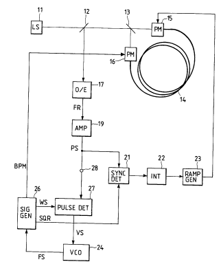
3 5 Fig . 4 shows an embodiment of the present
invention depicting parts corresponding to those shown in
Fig. 1 using the same numerals. In the present
_7_ 2045743
invention, a signal generator 26 generates a bias phase
modulation signal BPM which is stepped up by a magnitude
Vb corresponding to a phase shift of T/2 radian at every
time interval T for n steps (for example, n = 3 in
5 Figs. 5A and 5B) and then stepped down by said magnitude
Vb at every time interval T for n steps, as shown in Row
A of Fig. 5A Said phase modulation signal BPM actuates
a biasing phase modulator 16. Therefore, when the time
interval T is equal to a propagation time r through an
10 optical fiber coil 1~, a phase modulation CWP received by
a clockwise light ray returned to a beam splitter 13 in
the state of a zero input angular rate becomes as shown
in row B of Fig. 5A, while a phase modulation CCWP
received by the counterclockwise light ray delays by the
15 time interval T = T f rom the phase modulation CWP
received by the clockwise light ray, as shown in Row C of
the same figure. Consequently, the phase difference PD
between both light rays alternately takes 7r/2 radian and
-7r/2 radian at every nT (n = 3 ), and the transition in
20 the phase difference also occurs every point where the
bias phase modulation signal BPM starts either increasing
or decreasing.
Therefore, the signal generator 26 generates a
rectangular reference signal SQR in synchronization with
25 a phase difference signal PD between both light rays as
shown in Fig. 5A, in a period of 2nT, with which an
output PS of an amplifier 19 is synchronously detected in
a synchronous detection circuit 21. In the case of T = T
with a zero input angular rate, an output FR from the
30 opto-electric converter 17 takes a stationary level as
shown in Row E of Fig. 5A, in the same manner as known in
the prior art. When an angular rate is entered in this
state, such a modulation as cancelling a phase difference
caused by the Sagnac effect between the clockwise and
35 counterclockwise propagating light rays is given to the
phase modulator 15, thereby the input angular rate is
measured .
-8- 2045743
In the case where the time interval T of the
biasing phase modulation signal is smaller than the
propagation time t through the optical f iber coil 14, a
phase modulation CCWP received by the counterclockwise
5 light lags phase modulation CWP received by the clockwise
light returned to the beam splitter 13, by T + ~T.
Consequently, the phase difference PD between both light
rays mainly takes T'/2 radian during a period where phase
modulations CWP and CCWP repeat the steps of +7r/2 radian
10 (increasing period). In the increasing period, however,
there are intervals ~T where the phase difference PD
becomes T radians at every T. Likewise, in a period
where phase modulations CWP and CCWP repeat the steps of
-T/2 radian (decreasing period), the PD mainly takes -T'/2
15 radian, although there are intervals ~T where the phase
difference PD becomes -T'/2 radian every T. In addition,
immediately after a transition between increasing and
decreasing periods, there is ~uch an interval of a length
~T in which a phase difference is zero. The output FR of
20 the opto-electric converter 17 takes a maximum, a minimum
and a stationary value when the phase difference is zero,
+T and =+7r/2, respectively. As a result, negative-going
pulses are created in the output FR of the opto-electric
converter 17 in the increasing and decreasing periods
25 as shown in Row E of Fig. 5B.
When the time interval T is larger than the
propagation time T, the phase modulation CCWP received by
the counterclockwi~e light lags by T - ~T from the phase
modulation CWP received by the clockwise light returned
30 to the beam splitter 13 with a zero input angular rate,
as shown in Fig. 5C. Phase differences PD of both light
rays mainly take T'/2 radian in an increasing period but
such an interval of a length ~T in which a phase
difference is zero, is repeated every T. Likewise, in a
35 decreasing period, the phase difference PD mainly takes -
T/2 radian but an interval of a length ~T in which the
phase difference is zero is repeated every T. Therefore,
A
.. . . .. . .
2045743
a pulse of a width ~T having a maximum level i8 created
every T. More explicitly, as shown in Row ~ of Fig. 5C,
a positive-going pulse is created in either an increasing
or a decreasing period.
According to the present invention, therefore,
it is detected using a pulse detector 27 whether there is
either a negative-going pulse or a positive-going pulse
in an increasing or decreasing period of the biasing
phase modulation signal sPM. If a negative-going pulse
is detected, a voltage controlled oscillator 24 is
controlled to have no negative-going pulses generated by
a detection output VS thereof. That is, an oscillation
frequency of the voltage controlled oscillator 24 is made
lower. When a positive-going pulse is detected, the
voltage controlled oscillator 24 is controlled
accordingly so that no positive-going pulses are
generated. That is, the oscillation frequency of the
voltage controlled oscillator 24 is made higher.
The pulse detector 27 can be composed as shown
in Fig. 6 for example. More explicitly, an output PS of
the amplifier 19 in Fig. 4 is supplied to a non-reversing
input terminal of a comparator 31 and a reversing input
terminal of a comparator 32, from a terminal 28 after
cutting off DC by a capacitor 29 As shown in an
operation time chart of Fig. 7, an input signal PS to the
terminal 28 is DC-filtrated corresponding to 7r/2 radian
and -7r/2 radian and then compared to voltages +Vm and -Vm
in the comparators 31, 32. The voltages +Vm and ~Vm are
provided to prevent error operations owing to a phase
difference caused by the Sagnac effect. The absolute
value of said voltages is made larger than the absolute
value of an output corresponding to a phase dif f erence
caused by an expected steep angular rate input.
Referring to Fig. 7, a positive-going pulse is detected
by the comparator 31 and a negative-going pulse is
detected in the comparator 32. The width of an output
pulse from the comparator 31 or 32 is made constant, if
A
-lO- 2045743
80 required, in a oneshot circuit 33 or 34 and the output
pulse is supplied to a gate 35 or 36. A window signal WS
iB supplied from the ~ignal generator 26 to gates 35, 36
to take out pulses in an increasing period and decreasing
5 period for the biasing phase modulation signal BPM, while
blocking pulses generated at a transition portion between
an increa6ing period and a decreasing period.
Output pulses from the gate 35 are up-counted
in a counter 37 while down-counting output pulses from
the gate 36 in the counter 37. When the counter 37
down-counts in the zero state, it counts -1, -2, -3, ---.
A value counted by the counter 3 7 is converted to an
analog signal by a DA converter 38. Said analog signal
is added to a reference signal Vr in an adder 39 as a
compensation signal. An output VS from the adder 39 is
supplied to the voltage controlled oscillator (VS0) 24 as
a control signal.
In the state of T ~ ~, as shown in Fig. 5B and
the left.side of Fig. 7, a negative-going pulse is
created in the output PS of the amplifier 19. Said pulse
is down-counted in the counter 37 providing a certain
negative value as a counting of the counter 37.
Corresponding to said counted value, a negative analog
signal is supplied to the adder 3 9 making a control
voltage to the VC0 24 smaller than Vr in order to lower
the oscillation frequency of the VCO 2~. Consequently,
time interval T becomes longer and, when T = ~, negative-
going pulses go out while maintaining such a state.
In the state of T > ~ to the contrary, as shown
in Fig. 5C and the right side of Fig. 7, a positive-going
pulse is created in an output PS of the amplifier 19, and
up-counted by the counter 37 providing a certain positive
value of counting by the counter 37. According to said
counted valuer a positive analog signal is supplied to
the adder 39 to make the control voltage to the VC0 24
larger than Vr~while increasing the oscillation frequency
2045743
of the VCo 2g Consequently, the time interval T is made
shorter and, upon T = T, no positive-going pulses are
generated while holding such a state.
Fig. 8 shows a practical composition of the
5 signal generator 25 in case of N = 3 like Figs. 5A, 5B
and 5C and the operation thereof is shown in the time
chart of Fig. 9. A signal FS of a period T issued from
the voltage controlled oscillator 24 is given to a clock
terminal CK of the up-down counter 41 which provides a
10 counted value "QlQo" to the D-A converter 42. The D-A
converter 42 issues analog voltages zero, V(~r/2), V(T)
and V(37r/2) with input values "QlQo" of "00", "01", "10"
and " 11 " respectively Said voltages provide the
clockwise light and t~Le counterclockwise light with phase
15 shifts of zero, 7r/2, T and 3T/2 raaians, respectively A
counted value QlQo of the counter 41 is applied to a NOR
gate 43 and an AND gate 44, the outputs of which are
given to a set terminal S and a reset terminal R of a
flip-flop 45, respectively. As a result, the flip-flop
20 45 is set only with the counted value "QlQo" of "00", and
is reset only with a counted value "QlQo" of "11". With
values other than the above, the flip-flop maintains its
previous state. The up-down counter 41 up-counts pulses
of an input signal FS when the Q output of the flip-flop
25 45 is at a high level, while down-counting with a Q
output at a low level. Consequently, when a counted
value ~'QIQo'' of the counter 41 becomes "00", the counter
41 enters an up-count mode, in which the voltage of the
phase modulation signal BPM, an output of the DA
30 converter 42, steps up every period of T as shown in
Fig. 9 in order to seqll~nti~lly up-count pulses of the
input signal FS. When the counted value "QlQo" thereof
arrives at "11", the flip-flop 45 is reset to set the
counter 41 in a down-count mode in which pulses of the
35 input signal FS are seqll~nt ~ y down-counted.
Therefore, the ~oltage of BPM, an output of the DA
converter 42, steps down every period of T.
A
~ . . ... .. . . ..
-12- 2045743
The Q output of the flip-flop 45 becomes a
rectangular wave of a period 2nT (= 6T) as shown in
Fig. 9. As the flip-flop 46 reads said Q output in the
period T of the input signal FS, the same waveform as the
5 Q output waveform of the flip-flop 45 is obtained in the
Q output, in a phase delayed by the period T. The Q
output of the flip-flop 46 is applied to a synchronous
detector 31 as a reference signal SQR. The outputs of
the gates 43 and 44 are entered into an XOR gate 47. The
XOR gate 47 produces an output of a signal waveform in
which its level becomes low during a period where either
a reset signal or a set signal is given to the flip-flop
15 45 and elsewhere the level becomes high as shown in
Fig. 9 Said signal waveform is read into the flip-flop
48 by a reversed pulse of the input signal FS, so a
wavef orm obtained in the Q output is such that the output
20 waveform of the XOR gate 47 is delayed by T/2. The
waveform thus delayed forms a window signal WS as a level
thereof becomes low only during a period T with a center
of either a rising edge for the waveform of the phase
modulation signal BPM to begin increasing or`a falling
25 edge for the same to begin decreasing.
According to the present invention as described
above, the phase modulation signal in use is such that
the increasing of a magnitude giving a phase shift of 7r/2
radian every time interval T is repeated for n steps and
30 then the decreasing of a magnitude to give a phase shift
of 7r/2 radian every time interval T is repeated n steps.
In an increasing period and a decreasing period of the
biasing phase mDdulation signal, it is detected whether
there is either a positive-going pulse or a negative-
35 going pulse. If there is a positive-going pulse, the
time interval T is shortened accordingly in order that
positive-going pulses no longer occur. When there is a
negative-going pulse, the time interval T is shortened
correspondingly so that negative-going pulses disappear.
~ .
_, , , .. _ . _ ... . . , . _ _ _
-13- 2045743
The method of the present invention is unlike
conventional systems where a relative timing of pulses is
detected to deter~ine whether the pulses are leading or
lagging from an edge of the phase modulation signal.
5 Instead, the method of the present invention
discriminates whether a pulse is a pos~tive or negative
going one. Therefore, the time interval T can be made
precisely in agreement with the propagation time T no
matter whether the waveform of pulses is distorted or the
10 timing thereo~ ie delayed because the frequency band of
the opto-electric converter 17 is not wide enough