Note: Descriptions are shown in the official language in which they were submitted.
EHF ARRA~ ANTENNA BACKPLATE
B ACKG~OIJND
The present invention relates to a phased array aneelma and, more p~articularly,to methods for constructing and apparatus comprising the backplaLe of phased arrays
that incorporate active electronic modules.
Present trends are tO provide advances in phased array antennas for the EHF or
S rnillimeter wave frequency band. This band is roughly from 30 - 300 GHz, which cor-
responds to a wavelength of lcrn - lmm. The goal is to provide high power, light-
weight and low cost antennas ~or the EHF band. Antenna arrays at the EHF band in-
corporate heat producing devices in the backplate thereof. These heat ~roducing de-
vices may include GaAs FET diodes, hybrid circuits, MMIC chips, VHSIC gate ar-
10 rays, monolith;c sub~rrays or other types of semiconductor devices or modules. Heatis also produced by RF transrnission and distribution devices such as ~eed ne~wo~ks,
planar waYegu;de power dividers, and the like. Furtherrnore, heat is also produced by
the DC power distlibution and buffering, as well as by control logic signal distribution
and processlng.
The complete antenna array with its backplate comprises a miniaturized structurehaving multiple layers. The purpose of the array backplate is to provide EHF signal
distribution, DC power distribut;on, logic signal d;stribution, thermal management, and
structural rig;d;ty for subarray modules to be mounted thereon. It is desired that the
EHF signal distribution be effic;ent (low signal loss), simple and highly reliable. It is
20 also desired that the backplate be thin and light in weight. In particular, a thickness of
0.5 inch facilitates low profile rrlounting of the antenna array on aircraft.
., ~ , . . - . .
- , : :, . ..
.
:,. . . : ~ ., . : . ,
-. " ,:
. . .
3 ~ ~
It is an objective of the present invention tO reduce or elirnina~e ~he large number
of thermal contact interfaces usually found in the cooling systems of conventional array
backplates. It is also an objective to provide an array backplate that eliminates or re-
duces the high parts count typically found in conventional array backplates. Another
objective is the provision of an array backplate that does not require a labor-intensive
manufacturing process.
SUMMA~Y OF THE IN~ENTION
In accordance with these and other objectives and features of the present inven-tion, there is provided a novel EHF array antenna backpla~e that integrates the thermal
cooling structure and the signal processing structure together into one unified structure.
In airborne applications, forced air is employed to conduct heat from the active rnod-
ules; while in spaceborne applications, metal matrix composite materials or heae pipes
are employed. The array backplate is a very simple structure that is comprised of only
four layers. The layers are: a high density multichip interconnect board, a metal matrix
composite mo~herbo~rd, an integrated waveguide/cavity/cooling structure, and a metal
matrix composi~e baseplate. The backplate accommodates various types of subarraymodules. The DC and logic lines of each sub~ray module use solder bumps to con-
nect to the high density multichip interconnect board where DC power and control logic
signal distribution takes place. The base of the subarray modules is soldered in four
locations to the metal matrix composite motherboard through openings in the high den-
sity mul~ichip interconnec~ board. This provides structural rigidity and facilitates heat
dissipation from the active rnodules.
EHF signals are electromagne~ically coupled to the subarray modules from a
resonan~ cavity via probes th~ are attached to the subarray modules and which pro~ude
through the high density mul~ichip interconnect board. Probes are strategically located
in the resonan~ cavity to pick up the EHF standing wave generated by slots provided in
the floor of the cavity. The slots are part of a slotted waYeguide EH~ 16-way power
divider network that only has 0.023 dB attenuation per inch. Total insertion loss from
the EHF feed to the subarray modules via 256 power divisions is approximately 25.8
dB. In a backplate used for signal reception rather than transmission, the EEIF signal
distribution works using the same principle~ only the signals travel in the reverse direc-
tion. Two openings are provided at the side of the waveguide/cavity/cooling structure
through which cooling air is fed into ~he reson~mt cavities. This ~echnique is an effi-
cient impingement air cooling system. The waveguide/cavitylcooling structure is also
the primary load-bearing member of the backplate. In space b~me applications, the air
cooling system is replaced with imbedded heat pipes or matrix compos;te materials.
.:
f~
BRI~iF DESCRIPTION OF THE DRAWINGS
The various features and advantages of the present invention may be more read-
ily understood with reference to the following detailed description taken in conjunction
with the accompanying drawings, wherein like reference numerals designate like struc-
5 tural elements, and in which:
FIG. 1 is an exploded view of an array backplate in accordance with the inven-
tion showing the four principal structural layers thereof;
FIG. ~ is a plan view of an EHF array antsnna backplate showing a plurality of
subarray active modules disposed thereon;
FIG. 3 is an enlarged cross section of a portion of the array backplate shown inFIG. 2 taken along the lines 3-3;
FIG. 4 is a perspective view of the combined waveguide and resonant cavity
and cooling structure with its cover removed;
FIG. 5 is a bottom view of the third layer of the backplate showing the 16-way
power divider network below the floor of the resonant cavities;
FIG. 6 is a diagram illustrating the distribution of signals and cooling air in the
array backp}ate, FIG. 6a showing the control logic signal and DC power distribution,
and FIG. 6b showing the EHF signal and cooling air distribution;
FIG. 7 is a cross-sectional view of a second embodiment of an array backplate
employing imbedded heat pipes for cooling active rnodules; and
FIG. 8 is an enlarged view of a portion of the embodiment of the backplate of
FIG. 7 showing details of one of the active modules.
DETAILED DESCRIPTION
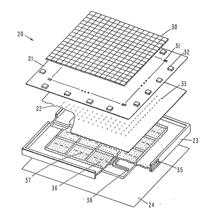
Refemng now to FIG. 1 of the drawings, there is shown an exploded view of
an array backplate 20 cons~ucted in accordance with the principles of the present in-
vention. The array backplate 20 is a very simple structure that is comprised of four
main structural layers 21, 22, 23, 24. The first layer 21 is a high density multichip in-
terconnect board that provides distribution of control signals and DC power on a multi-
layer substrate. The second layer 22 is a metal matrix composite motherboard that pro-
vides a substrate for the physical support of active serniconductor elernents. The third
layer 23 of the array backplate 20 is a combined or integrated waveguide and resonant
cavi~y and cooling stmcture. The third layer 23 is also the primary load-bearing mem-
ber of the backplate 20. The fourth layer 24 is a metal rnatrix composite basepla~e
which serves as a cover plate for the backplate 20.
As shown in FIG. 1, an alray of subarray modules 30 is provided, and in the
present example, there are 256 modules 30 arranged in a 16 x 16 aIray. The first layer
,~. . . .
'- : . ' :
:
':
21, which is direc~ly below the modules 30, is provided with coupling means 31 for
each module 30, the coupling means 31 including thermal vias and solder bumps. The
DC power and logic lines of each module 30 use solder burnps tO connect to the high
density multichip interconnect board where DC power and control logic signal distribu-
S tion take place. Around the outer periphery of the first layer 21, there are provided aplurality of support modules 32, which may include buffers and power conditioners for
processing the DC power and logic control signals. The second layer 22 is provided
with a plurality of openings 33 which selve as vertical feedthrough holes for EHF sig-
nal probes, and there is an opening 33 for each subarray module 30. The third layer 23
10 is provided with a plurality of air holes 34 in the interior thereof, and cooling air in-
put/output ports 35 around the exterior thereof. The third layer 23 is also provided
with a plurality of resonant ca~ities 36, there being 16 resonant cavities 36 in the pre-
sent exemplary embodiment. Each resonant cavity 36 has coupling slots 37 for cou-
pling to an EHF planar slotted waveguide 16 way power divider network 38 disposed
directly below the floor of the resonant cavities 36.
In this embodiment of the array backplate 20, the arrangement of the four struc-tural layers 21, 22, 23, 24, the EHF feed power divider networks 38, and the cooling
system components allows the simultaneous EH:F signal distribution and air cooling
funct;on to be accomplished in a single structure, namely the third layer 23. In this
embodiment, the forced cooling air is channeled through the EHF resonant cavity 36 to
directly cool the heat source while maintaining high EHF signal efficiency and high
thermal efficiency. This ernbodiment of the invention also allows the array backplate
20 to be thin and lightweight because it avoids using cold plates, heat si~s and cooling
fins such as are used in conventional EHF array backplates.
FI&. 2 is a plan view of an EHF array backplate 20 having a plurality of active
subarr.~y modules 30 disposed thereon. FIG. 3 is an enlarged cross-section of a por-
tion of the array backplate 20 shown in ~;IG. 2 taken along the lines 3-3. The active
subarray module 30 is above and connected to the ~Irst layer 21 which is the high den-
sity multichip interconnect board that distributes DC power and logic control signals.
However, the module 30 is physically fastened to and supported by the second layer
22, the metal matrix composite motherboard, by means of solder connecdons 40 which
pass through openings provided in the first layer 21. Speci~lcally, the base of the sub-
array module 30 is soldered in four locations to the metal matrix composite mother-
board. This providP~s structural rigidity and facilitates heat dissipation from the module
30. A coupling means 31 on the first layer 21 includes a thermal via for heat conduc-
tion from the module 30 to the second layer 22. I'he subarray module 30 is provided
with a radiadng element 41 for radiating EHF signals outwardly from the array back-
. -
plate 20. An EHF probe 42 extends through the opening 33 in the second layer 22 to
couple into the resonant cavity 36. The openirlg 33 rnay be filled with Teflon around
the EHF probe 42. A slotted waveguide 43 couples EHF signal energy into the reso-
nant cavity 36 by means of the coupling slot 37. Air cooling holes 44 are provided in
the third layer 23 to permit air 45 to circulate below the subarray module 30.
FIG. 4 shows a simplified view of the interior of one of the resonant cavities 36
Wit}l its cover opened and lifted off of it. The cover comprises the combined ~rst layer
21 and the second layer 22 and the subarray modules 30 that are comlected electrically
and physically thereto. FIG. 4 shows the EHF pick-up probes 42 protruding ~roughthe openings 33 provided therefor in the second layer 22. The slotted waveguide 43
which is a part of the 16-way power divider network 38 passes beneath ~he floor of the
resonant cavity 36. The mode excitation coupling slots 37 couple the EH~ energy from
the slotted waveguide 43 into the resonant cavity 36 setting up standing waves 46 in a
predetermined standing wave pattern. When the cover is closed, the probes 42 arestrategically located in the resonant cavity 36 to pick up the EHF standing wave 46 gen
erated by the slots 37 in the floor of the cavity 36. The slots 37 are acLually a part of
the slotted waveguide 43 which is in turn a paut of the EHF 16-way power divider net-
work 38. The EHF signal distribution arrangement just described may be considered
to be a non-physical, resonator fed, distribution means for the EHF signal. This non-
physical, resonator-fed arrangement is low-loss, simple and insures high reliability.
FIG. S is a bottom view of the third layer 23 comprising the integrated waveg-
uide, cavity, and cooling structure, showing the low-loss, planar slotted waveguide
EHF 16-way power divider network 38. The power divider network 38 employs a
plurality of high isolation, short block 3 dB hybrids 47. The EHF planar waveguide
power divider network 38 constructed with the 3 dB hybrids 47 has low-loss and pro-
vide excellent isolation between ports. Typically, the power divider network 38 has
only 0.023 dB attenuation per inch, and the total insertion loss from the EHF feecl to
the subarray modules 30 via 256 power divisions is approximately 25.8 dB.
The foregoing description of the E~IF signal feed applies to an array backplate
20 when used to transmit EHF signals. When an array backplate 20 is adapted to re-
ceive EHF signals instead of transmit, it opera~es on the same principles7 except that the
signals travel in the reverse direction.
FIG. 6 is a schematic diagrarn in block form illustrating signal flow an~l cooling
air flow in the array backplate 20 of the present invention. FIG. 6a shows the control
logic signal and l~C power distribution. An aircraft on which the EHF antenna array is
installed has a DC power source 50 connected by a cable 51 and connector 52 to the
second layer 22 of the array backplate 20 which comprises the metal matrix composite
-
.
: - , - . .;
. ~
6 ~ f~ ~ ~
motherboard. Similarly, a central processing w~it (CPU) 53 is connected by way of a
cable 54 and connector 55 to the second layer 22 of ~he array backplate 20. The DC
power and control logic signals pass through vertical feedthroughs 56, 57 to the first
layer 21 which is the high density multichip intercoMect. 'rhere, the DC power and
5 control logic signals are routed to support modules 32 which comprise power condi-
tioners and bu~fers. From the support modules 32, the DC power and control logicsignals are distributed to the 256 subarray modules 30.
Referring now to FIG. 6b which shows the EH~; signal and cooling air distri-
bution, a communication system 60 provides an !EHF signal via an EHF waveguide 61
10 to the EHF 16-way planar waveguide power divider network 38. The EHF signal is
distributed to the 16 resonant cavities 36. The 256 probes 42 couple the EHF signal
energy to the 256 subarray modules 30 for radiation away from the backplate 20. A
source of forced air (not shown) provides air to an input port h2 of the resonant cavities
36. The air exits the resonant cavities 36 via an output port 63.
The embodiment of the invention described above exemplifies a unique back-
plate technology that is useful in the field of EHF phased array antennas having a plu-
rality of heat dissipating active modules. It is a feature of the present invention that the
backplate technology incorporates a unique integrated approach in which the thermal
structure and the RF distribution structure are combined together into one unified
20 structure. The invention is not limited to the embodiment described above in which
forced air is employed to conduct heat from the active modules.
Referring now to FIG. 7, there is shown an embodiment of an EHF array
backplate 70 employing heat pipes 71 to conduct heat away frorn active modules 72.
This embodiment of the present invention is useful both in space and airborne applica-
25 tions. The EHF signal distribution is accomplished by means of a resonant cavity 73.FIG. 8 shows an enlarged view of a portion of the embodiment of the backplate 70 of
FIG. 7 illustrating details of one of the active modules 72. The active module 72 is il-
lustrated as being a monolithic microwave integrated circuit (MMIC) although the back-
plate 70 may be adapted for many other types of active module 72. As may be seen in
30 FIG. 8, the heat pipes 71 are imbedded in the wall of the structure that forms the reso-
nant cavity 73. The active module 72 has a Mdiating element 74 and an EHF signalprobe iS that protrudes into the cavity 73. The probe 75 typically is surrounded by a
Teflon member 76.
Thus there has been described a new and improved EHE array antenna back-
35 plate that allows simoltaneous EHF signal distribution and module cooling functions tobe accomplished in a single structure. The non-physical resonator-fed signal dis~ibu-
tion arrangement is low-loss, simple, and insures high reliability. The cooling system
c~ ~
interposes a minimal number of thermal contact in~erfaces which results in an effi1cient
thermal manag,ement system. In airborne applications, forced air is used to conduct
heat from the active modules, while in space borne or airborne applications, metal ma-
trix composite materials or imbedded heat pipes are employed to conduct the heat away
5 from the active modules. It is to be understood that the above-described embodiments
are merely illustrative of some of the many specific embodiments which represent appli-
cations of the principles of the present invention. Clearly, numerous and other arrange-
ments can be reaclily devised by those skilled in the art without departing from the scope
of the invention.