Note: Descriptions are shown in the official language in which they were submitted.
20~615S
1083-2
METHOD AND COUPLER FOR INTERFACING A PORTABLE
DATA CARRIER WITH A HOST PROCESSOR
BACKGROUND OF THE INVENTION
The invention relates to a method and coupler for serial
5 communication between a Universal Asynchronous Receiver Transmitter
terminal (UART) such as, would be associated, for example, with a host
processor, a personal computer, or point of sale device or the like and a
portable data carrier.
DESCRIPTION OF THE PRIOR ART
A portable data carrier is a portable device which contains
integrated circuit(s). Examples of portable data carriers are Integrated Circuit
Cards, data keys, smart cards, and smart coins. Recent advances in the
manufacture of integrated circuit chips have led to the development of a
multipurpose plastic card having a microprocessor no bigger than a penny
15 embedded therein known as a "smart card". Such cards and their method of
manufacture and methods for transmitting signals between the cards and the
host terminal are well known.
Because of the built-in computer logic and memory, the so called
"smart card" has found use in a variety of applications. The "smart card" can
20 be used for encoding confidential data, as an electronic security key for
protecting information and property, a portable file for monitoring medical or
insurance records, payroll records, funds transfers and inventory controls, to
name a few.
Despite the popularity of portable data carriers containing
25 integrated circuits such as, for example, the so-called "smart cards", heretofore
20~61~5
it has been thought necessary when coupling such devices serially to a host
terminal that the coupler or smart card reader must contain a microprocessor
and that "bit banging" of the input and output signals was the only way to
process the input and output. In such arrangements, the microprocessor in
5 addition to processing the inpuVoutput signals is also responsible for developing
the major control and interface signals to enable communication.
Couplers for Integrated Circuit Cards interface to host processors
or terminals, simply is referred to as hosts, using a number of different serial
l/O channels and communication protocols. Commands from the host are
10 transmitted to the coupler over the serial l/O channel as a series of bytes.
Handshake lines of the serial l/O channel are sometimes used by the host, but
only to control the flow of commands to the coupler, not to control the
coupler/card interface. The presence of an Integrated Circuit Card in the
coupler is sometimes reported to the host using a serial l/O channel handshake
1 5 line.
All couplers available today contain a processor, such as an 8051,
which controls the card interface and accepts commands from the host.
Because the microprocessor receives characters from the host processor and
retransmits them to the Integrated Circuit Card, a performance penalty is
20 imposed. A major penalty or disadvantage of such couplers is that the
microprocessor in the coupler interface slows down the process of interfacing
the smart card to the host terminal. This is due to the fact that for
transmissions from the host terminal, the microprocessor has to "listen" for a
command from the host terminal and then interpret and reformat the command
2~46155
before sending it to the smart card. The same would be true when the smart
card transmits a message to the host terminal. The microprocessor has to
receive the message, reformat the message and then transmit the reformatted
message directly. A system which can avoid the use of a microprocessor
5 would process information two-to-three times faster.
Another disadvantage of known systems is the cost resulting from
the necessity of incorporating a microprocessor in the coupler. A system which
avoids the use of a microprocessor would provide a substantial cost benefit.
SUMMARY OF THE INVENTION
Accordingly, it is a primary object of the present invention to
provide a coupler as an interface between a portable data carrier and a host
information processing terminal which avoids the use of a microprocessor.
Another object of the present invention is to provide a coupler as
an interface between a portable data carrier and host processor including a
15 means of communicating with the portable data carrier over a serial l/O
communications channel without the coupler receiving and retransmitting
characters communicated between the portable data carrier and the host
processor.
A further object of the present invention is to provide a coupler as
20 an interface between a portable data carrier and host processor which controls
portable data carrier interface signals using handshake lines of a serial l/O
communications channel.
Yet another object of the present invention is to provide a coupler
as an interface between a portable data carrier and a host processor wherein
2046155
said coupler is powered with electrical power parasitically derived from a serial
l/O communications channel.
Still another object of the present invention is to provide a coupler
as an interface between a portable data carrier and a host processor which
5 includes a means of enabling required electrical signals when the portable data
carrier's presence is detected.
A further object of the present invention is to provide a coupler as
an interface between a portable data carrier and a host processor which
provides sequences of electrical signals such as RESET signals when a
10 portable data carrier's presence is detected.
Another object of the present invention is to provide a coupler as
an interface between a portable data carrier and a host processor in which
received and transmitted data from the host processor is connected with data
transmitted by the portable data carrier to allow detection of error signals
15 generated by the portable data carrier.
Still another object of the present invention is to provide a coupler
as an interface between a portable data carrier and a host processor which
includes a means of connecting received data from the host and data
transmitted from the host processor with data transmitted by the portable data
20 carrier to allow the host processor to receive its own transmissions and detect
errors in communication.
A further object of the present invention is to provide a coupler as
an interface between a portable data carrier and a host processor which
includes a connecting means which replaces the conventional interface driver
20~615S
and receiver integrated circuit(s) of a host processor communications device.
A still further object of the present invention is to provide a device
for interfacing one or more portable data carriers by which the communications
of each portable data carrier and a local or host processor are combined with
5 the communications of each other portable data carrier or local or remote
processor, such transmissions being receivable by the other portable data
carriers and local or host processors, if any.
Yet another object of the present invention is to provide a low cost
solid state coupler as an interface between a portable data carrier and a host
10 processor which avoids the use of a microprocessor in the coupler and
retransmission of characters communicated between the portable data carrier
and the host processor.
In accordance with a preferred embodiment of the invention, a
coupler for interfacing a portable data carrier with a host processor comprises
15 first terminal means adapted to receive data from the host processor,
inpuVoutput terminal means adapted to receive input data from the data carrier
and the data received at the first terminal means from the host processor,
second terminal means connected to said inpuVoutput terminal means to
enable the input data from said data carrier to be translated to the host
20 processor and control means connected between said first and said second
terminal means and said inpuVoutput terminal means for translating input data
from said first terminal means to said second terminal means and to the
inpuVoutput terminal means.
In accordance with this embodiment, input data is looped back
20~61SS
between the first and the second terminal means and the control means
comprises switching means for switching data to the second terminal means
and the inpuVoutput terminal means.
Card connector means may be provided for receiving the portable
data carrier along with means for controlling its switching means for applying
a bias voltage to said control means in response to insertion of said data carrier
into said connector means.
In a further variation of the system, means are provided for
receiving data from the host processor and translating said data to the
inpuVoutput terminal means adapted to be connected to said data carrier and
simultaneously echoing the data received to the host processor.
The system further includes means for connecting data from the
portable data carrier to the inpuVoutput data terminal means and means
responsive to the connection of said data carrier to the inpuVoutput terminal
1~ means for generating control signals to enable translation of data from the data
carrier to the host processor and data from the host processor to the data
carrier. Feedback means assures echoing the data received from the host
processor back to the host processor to allow said host processor to receive
its own transmission.
The invention also relates to a method for interfacing a portable
data carrier with a host processor via a signal coupler comprising the steps of
generating a carrier present signal CRD PRS and a clear to send signal CTS
upon insertion of a portable data carrier in a connector adapted to receive saidcarrier; generating a CRD ON signal in response to a request to send signal
~046155
from said host processor after receipt by the host processor of a clear to send
signal; generating a card voltage signal CRD VCC to be applied to the portable
data carrier in response to said CRD ON signal and transmitting and receiving
data between said host processor and portable data carrier, said step of
5 transmitting and receiving data including the step of echoing data from the host
processor to allow said host processor to receive its own trans,nission for
detecting errors in communication.
A further variation of the method further includes generating a
clock signal CRD CLK in the coupler and applying the clock signal to the data
1 0 carrier.
According to the inventive method, the received and transmitted
characters of the data to detect multiple bit errors are compared and
retransmis- sion of characters transmitted by the data carrier is ordered upon
detection of an error.
In accordance with a specific arrangement of the present
invention, the coupler is connected to a host processor via an EIA-232N.28
serial l/O channel which provides Clear-To-Send (CTS), Request-To-Send
(RTS), Data-Set-Ready (DSR) and Data-Terminal-Ready (DTR) signals as well
as Transmit-Data (TX) and Receive- Data (RX). The host will include a
20 universal asynchron- ous receiver transmitter (UART) which may be hardware
or software and is assumed to be a Data Terminal Equipment (DTE) device,
while the coupler acts as a Data-Com- munications-Equipment (DCE) device.
Other forms of serial link such as RS-422 and Integrated Services Digital
Network (ISDN) protocols can also be used.
20~615~
The coupier provides a means of coupling the TX and RX lines
to the l/O line of the Integrated Circuit Card. Feedback means may be
provided between the TX and RX lines to be used for error detection. In full
duplex Integrated Circuit Cards, the TX and RX lines are connected to the
5 corresponding Integrated Circuit Card contacts of the Integrated Circuit Cards.
Of course, contactless interfaces are also possible.
In accordance with the present invention, circuit means is provided
which detects the presence of an Integrated Circuit Card in the coupler's card
connector. A further circuit means is provided to couple this signal to the card
present CTS line of the EIA-232/V.28 link to provide card present CTS signals
to the host indicating that a card is present in the coupler. The host commands
the coupler to raise or lower the card's RESET line by asserting or clearing the
DTR signal, while the coupler provides means for controlling the RESET line
in response to the state of the DTR signals. The RESET line is qualified with
15 CRD VCC.
The RTS signal is used by the host observer to request the CRD
VCC be raised or lowered. The Coupler provides a means of controlling CRD
VCC in response to the RTS signal. In addition, the coupler may qualify this
signal with the presence of a card in the connec- tor. The coupler further
20 provides a means of enabling a clock signal to the CRD CLK contact of the
Integrated Circuit Card when RTS is active. The coupler further provides a
means of enabling CRD VPP when RTS is active. Thus RTS controls CRD
VCC, CRD VPP and CRD CLK.
The coupler can provide a means of controlling DSR to reflect the
204615S
status of coupler power. This is used as a diagnostic tool to detect the
presence of a working coupler.
CRD CLK, CRD VCC, and CRD VPP can be controlled
independently using additional handshake lines. In addition, the coupler can
5 include a means of providing a suitable RESET pulse when RTS requests that
CRD VCC be raised to a card.
Further, the CRD VCC, CRD CLK and CRD RESET may all be
provided by the coupler when a card is inserted. This embodiment has
particular application in access control applications where the couplercommuni-
10 cates with a host processor via a current loop inter- face. In this case no
handshake lines need to be run to the access control portal. The presence of
a card is signaled to the host processor by the card's Answer-To-- Reset.
Power to the coupler can be provided by an external supply, a
battery, a connection in common to the EIA-232N.28 channel, or by
parasitically removing power from the EIA-232N.28 channel. The latter has the
advantage of simplicity and low cost but restricts the coupler to low power
Integrated Circuit Cards. Other types of serial l/O channels can also be tapped
for power.
Power and the required EIA-232N.28 signals can be provided to
20 the coupler if a cable which connects the coupler to the host processor is
terminated such that it connects directly to a socket (or sockets) which normally
house the EIA-232/V.28 driver and receiver integrated circuit(s). In this case
the signal levels are typically TTL, not EIA-232/V.28 and power is directly
available. This provides a very low cost option as it reduces the circuitry in
2û4615S
both the host and coupler for level conversion, and alleviates the need for a
special power supply. This is the preferred approach for couplers which are
added within the housing of an existing host processor, such as within the disk
drive bay of a PC.
ISO has standardized a communication protocol for integrated
circuit cards which uses a unique byte retransmission request bit (UGON
++++). A retransmis- sion bit is sent by the receiver of a character when the
character has been received in error. The transmitter then retransmits the
erroneous character. The protocol is designed to be incompatible with a
standard Universal Asynchronous Receiver Transmitter as is used on most
asynchronous l/O channels today. The retransmission bit must be transmitted
during what is normally the stop bit of the transmitted character. A normal
Universal Asynchronous Receiver Transmitter (UART) may see this as a start
bit, but would not report it to the host until a full 12 Elementary Time Units
(ETUs) of character time has elapsed. The transmitter may well be into the
transmission of a new character before the error report is detected, resulting in
a communications collision.
In accordance with a particular object and advantageous feature
of the present invention, there is provided feedback within the coupler between
the TX and RX EIA-232N.28 lines. This allows the host to receive it's own
transmissions. If the card signals that a retransmission is requested, then the
UART reports a framing error as the retransmission bit is within the normal stopbit of the character is question. In addition, if a double bit error is produced on
the line and the Integrated Circuit card does not detect the error the host can
2046155
still detect the error by comparing the received and transmitted characters.
This provides a robust means of error detection for the host. In the case of
errors in characters transmitted by the card, the host can detect these using the
parity bit, and once an error has been detected in a transmission the entire
5 command can be repeated to ensure valid data. Once a transmission protocol
which includes block error detecting codes, error detection and correction
becomes more conventional with retransmission at the block level.
Multiple cards can be connected together to share a single serial
l/O channel. In this case, each card can receive the transmissions of any other
10 cards on the channel as well as any host processor(s) or local processor(s) on
the channel (if any). A host processor (or processors) or local processor (or
processors) on the channel can receive the transmissions of any cards or other
processors on the channel. Collisions on the communications channel are
resolved by an appropriate Integrated Circuit Card communications protocol, or
15 additional handshake lines.
BRIEF DESCRIPTION OF THE DRAWINGS
These and other objects and advantages of the invention will
become readily apparent to those skilled in the art from the detailed description
of the preferred embodiments to be considered in connection with the following
20 drawings, wherein like reference characters represent like parts throughout the
several views.
Figure I shows a typical system configuration of the present
invention in block diagram form.
Figure 2 shows a typical UART configuration within a host
20461~5
processor for serial l/O communications with EIA-232N.28 level conversion.
Figure 3 shows a block diagram of the coupler in accordance with
the present invention.
Figure 4 shows a block diagram of the coupler in accordance with
5 the present invention in the case where the card enables and CRD RESET
pulse are generated in the coupler without host processor control.
Figure 5 shows a block diagram of the coupler in accordance with
the present invention in the case where there are two Integrated Circuit Card
Interfaces on the one coupler.
Figure 6 is a schematic diagram of the coupler in accordance with
the present invention.
Figure 7 shows a power supply for the coupler which in
accordance with the present invention parasiti- cally supplies +5 volts and +12
volts (typical) for coupler operation from the EIA-232N.28 input signals, without
destroying the signal integrity of the TX signal.
Figure 8 shows a typical layout of the card connector circuit board
and cable connectors for the present invention.
Figure 9 shows a typical asynchronous character frame as used
in the present invention, and
Figure 10 is a timing diagram of a transmitted character illustrating
how internally connecting the transmitted data from the host processor to the
card l/O line and the received data line of the host processor is used to detect
errors.
DESCRIPTION OF THE PREFERRED EMBODIMENT
20461~
Figure 1 shows a typical system configuration with a personal
computer acting as a host processor, 10, an EIA-232N.28 serial communication
line comprising an RS 232 cable 11 acting as a serial l/O channel, coupler 12,
and an Integrated Circuit Card, (ICC) 13, acting as the portable data carrier.
ICC 13 is a plastic card containing a micro processor 14 positioned on the card
in accordance with ISO nomenclature specification 7816. ICC 13 includes
contacts C1-C8 each of which is reserved in accordance with ISO 7816
standard for a particular signal. For example, card contact C1 receives a Svdc
card VCC voltage (CRD VCC), contact C2 receives the card reset signal (CRD
RST), contact C3 receives the card clock signal (CRD CLK). Card input and
output data are received and sent via card contact C7. Contacts C1-C8 are
connected within the coupler to contact terminals of a card connector J4. Card
Connector J4 includes a switch 15 (shown in Fig. 6) conveniently positioned
to be actuated to a closed position upon insertion of the card so as to provide
a card present (CRD PRS) signal to the host processor 10. Communication
with the host processor is maintained via a RS 232 serial communication line
11 connected to the host processor 10 which may be any type of terminal
adapted for serial communication and usually containing a UART which may be
either hardware or software. As shown in Fig. 1, host 10 may be a personal
computer including a display 16, data input keyboard 17 and processor 18.
Figure 2 shows a typical (UART) configuration within host
processor 10. The 8250 UART, 20, is common in many personal computers
and is the UART which corresponds to the software listings included in the
8250 Universal Asynchronous Receiver Transmitter. The UART 20 provides
20461~
and receives typical serial l/O communications channel signals, including a
transmit data to card signal TX, a receive data from card signal RX, a card
present signal CTS, an enable card VCC and CLK signal RTS, a reset card
signal DTR and a coupler power OK signal DSR. The latter signal is optional.
5 The sense of the control signals are as follows:
Card Present CTS = 0
Vcc ON RTS = 0
Card Reset DTR = 1
Coupler Active DSR = 0
The signals at the UART are at RS 232 levels and converted
through integrated circuit board U4 to TTL levels. Circuit board U4 may be a
MAX 236 available from Maximum Semiconductor and includes a plurality of
invertors connected as shown to ensure the proper sense and line of the
signals as shown in Fig. 2.
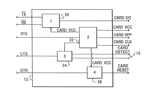
Figure 3 shows a simplified block diagram of the coupler 12.
Signals entering the coupler from the left, as viewed in Fig. 3, correspond to
the signals in Figure 2. Signals leaving the coupler 12 on the right, as viewed
in Fig. 3, correspond to connections to the Integrated Circuit Card 13 and a
card detection switch 15. Circuit means 30 are provided for coupling TX and
20 RX data signals from and to the host processor to CRD l/O.
A card VCC signal is derived from circuit means 32 which also
provides means for enabling a VPP signal and generating and enabling a card
clock CRD CLK signal under control of the host processor. The circuit
represented by block 34 provides means for reporting the presence of a card
14
~0461~
13 upon closure of the card detect switch 15 and generating a card present
signal CRD PRES applied to the CTS line and circuit 32. Circuit means 36
generates a card reset CRD RST signal in response to a data terminal ready
signal DTR and card VCC.
Figure 4 shows an alternate embodiment of the invention in the
case where the card enable control and CRD RESET pulse are generated in
the coupler 12 without host processor control. Circuit means 30 combines the
host processor TX and RX signals with the CRD l/O signal. It is enabled by
circuit means 32 which as hereinabove described provides a means of enabling
the CRD VCC, CRD VPP, and generating and enabling CRD CLK signals.
Circuit 32 is enabled by circuit 34 which responds to the presence of a card
and enables circuits 32 and 36. When a card is removed it powers down all
card contacts and circuit 36 is arranged to produce a low CRD RESET pulse
for a controlled period of time, then presenting a high CRD RESET state until
the card is removed.
Referring to Figure 5, there is shown a block diagram of the
coupler 12 in the case where there are a first and a second Integrated Circuit
Card Interfaces on one coupler. In this case, the combining means 30
combines the RX and TX signals from the host processor with the l/O lines of
both CRD l/O signals. In this case, each card receives the transmissions of the
other card and the host processor, and the host processor receives the
transmissions of both cards (assuming they are both present).
Referring to Figure 6, there is illustrated a detailed schematic of
the present invention. The card clock signal CRD CLK is developed by
20461~5
oscillator 40, comprising a Yl-3.5795 Mhz crystal 41, which is connected across
resistors 42 and 43. One end of resistor 42 is connected to pin 1 of invertor
44. The one end of resistor 42 has also connected thereto one end of
capacitor 45, the other end of which is connected to ground. The junction of
resistors 42 and 43 is connected between the output pin 2 of invertor 44 and
the input pin 3 of invertor 46. The other end of resistor 43 is connected to oneend of capacitor 47, the other end of which is connected to ground. Crystal 41,
resistors 42, 43, capacitors 45 and 47 and invertor 41, and pins 1 and 2 of
invertor 44 form a free running Pierce crystal oscillator circuit which developsa clock signal at the output. The output which is taken from pin 2 of invertor
44 is applied to pin 3 of invertor 46 where the clock signal is buffered. The
output of invertor 46 taken at pin 4 thereof is applied to one input of Nand gate
48. The other input of Nand gate 48 receives the CRD ON gate signal when
a request to send signal RTS is applied to pin 4 of U4 and the associated
invertor U4-5.
The request to send signal RTS which is applied to pin 4 of U4
is converted to a TTL level and its output taken from pin 5 of U4 and applied
to pin 5 of invertor 50. The output of invertor 50 taken at pin 6 thereof is
applied to one input of Nand gate 51. If pin 2 of Nand gate 51 to which the
signal is applied is at a 5 volt DC level and pin 1 has applied thereto a card
present CRD PRS signal at a 5 volt DC level, then pin 3 of Nand gate 51 will
go to ground. A smart card must be inserted in the connector and switch 15
closed before a CRD PRS signal will be available on pin 1 of gate 51 at a 5 voltdc level. Because Nand gate 51 is an open drain device, a pull up resistor 52
16
~0~6155
is connected from the output line of gate 51 to VCC. The output of Nand gate
51 is connected to pin 9 of invertor 53, the output of which taken at pin 8
thereof provides the CRD ON signal.
The CRD ON signal does three things. It is applied to the
5 powered up visual indicator circuit. To this end, CRD ONis applied to pin 13
of invertor 54. Output pin 12 of invertor 54 is connected through current limiting
resistor 55 to pin 4 of connector J3. Pin 4 has connected thereto a light
emitting diode LED which is returned to VCC via pin 3 of connector J3. Upon
insertion of a card into the card connector and consequent closure of switch 15,
10 light emitting diode connected between resistor 55 and VCC provides a visual
indication that CRD ON is at a 5 volt dc level. This provides the user with a
visual indication that the smart card is powered up. Secondly, the CRD ON
signal is applied to pin 5 of Nand gate 48. This switches the gate ON to
provide a card clock output signal CRD CLK at line 57. The card clock is
15 applied via series load current limiting resistor 58 to limit the current in case of
short circuit. Because Nand gate 48 is an open drain device, a pull up resistor
59 is connected between output pin 6 of Nand gate 48 and CRD VCC so that
the pull up is only active when CRD VCC is at a 5 volt dc level. The third
function of the CRD ON signal outputted from invertor 53 is to generate a CRD
20 VCC signal. This is to be distinguished from the VCC voltage developed by
regulator 70.
To this end, the CRD ON signal is applied to the CRD VCC circuit
comprising transistors 60 and 61, resistors 62, 63 and 64, and voltage regulator
65 CRD resistor 62 has one end connected to the base of transistor 60 and its
2 0 ~ 6 1 S ~
other end adapted to receive the CRD ON signal. The collector of transistor
60 is connected via resistors 63 and 64 to the emitter of transistor 61. The
junction of resistors 63 and 64 is returned to the base of transistor 61 and its
collector is connected to the input of voltage regulator 65, which provides a 5
5 volt dc regulated output CRDVCC signal applied to pin 6 of J4 and the C1
contact of the integrated circuit card.
When CRD ONis at ground level, transistor 60 is in its cut off
state and the base of transistor 61 is pulled to plus 12 volts dc through resistor
64 connected to a twelve volt source. This puts transistor 61 in cut off, and
10 nothing occurs. When a CRD ON signal at a 5 volt dc level is applied to the
base electrode of transistor 60, base current therein is limited and transistor 60
is put in conduction. In turn, the base of transistor 61 is pulled to ground
through series resistor 63 and transistor 61 switched into conduction. A 12 volt
dc signal appears on the collector of transistor 61 and is applied to the input of
voltage regulator 65. Voltage regulator 65 regulates the 12 volt dc supply to
plus 5 volts dc to establish the CRDVCC signal. This voltage is applied to the
smart card and several pull up resistors as hereinbefore described.
Power to the circuits is supplied through voltage regulator 70
which takes a voltage input from 7 volts dc to 30 volts dc and regulates it to a
20 5 volt dc. The input voltage to regulator 70 may be applied via an external plug
in jack J1. The VCC source 70 supplies power to other circuits in the coupler
but not to the smart card. To this end, VCC is applied to one contact of card
on switch 15, the other contact of which is connected to the RC circuit
comprising resistors 71 and 72 and capacitor 73. Capacitor 73 is connected
18
204615~
at one end to the junction of resistors 71 and 72 and at its other end to the
grounded end of resistor 72. When switch 15 is closed, due to the presence
of a card in the connector, the junction point 74 provides a card presence signal
CRD PRS which is applied to Nand gate 51 and to pin 11 of invertor 75.
Output pin 10 of invertor 75 is connected to pin 7 of U4 where it is converted
to an RS 232 level as the clear to send signal CTS. CTS is taken from pin 2
of U4 and connected to the host via the RS 232 cable. When the smart card
is withdrawn from the card connector, the CRD PRS line is pulled to ground by
resistor 72.
U4 and capacitors 76, 77, 78 and 79 form an RS 2321 TTL
voltage level shifter. This level shifter includes 4 invertors 1, 2, 3 and 4 which
convert TTL levels at terminals 18, 7, 6 and 19 of U4 to RS 232 levels at
terminals 1, 2, 3 and 24 of U4. Terminal 2 connects the clear to send signal
CTS to the host and terminal 24 applies the receive data signals RS to the host
converted to the RS 232 levels through U4 Shifter. U4 also includes 3 invertors
5, 6 and 7 which convert RS 232 signals from the host to TTL levels used in
the coupler. The request to send level RTS is applied to pin 4 of U4 and its
corresponding TTL level output taken at pin 5 is applied to input pin 5 of
invertor 50.
A request to send signal RTS from the host computer is applied
to pin 4 of U4 and converted to a TTL level. The signal is taken at pin 5 of U4
and applied to pin 5 of invertor 50. The output of invertor 50 taken from pin 6
thereof is applied to one input of Nand gate 51, the other input of which
receives a card present CRD PRS signal, If pin 2 of Nand gate 51 is at a 5 volt
19
2046155
dc level and pin 1 receives a CRD PRS signal at a 5 volt dc level, then the
output of Nand gate 51 will go to ground. A smart card must be inserted in the
connector before a CRD PRS signal is available.
A data terminal ready signal DTR from the host computer is
5 appHed to pin 16 of U4 and is converted to TTL level. This signal taken at pin
17 of U4 is applied to pin 9 of Nand gate 80. The other input of Nand gate 80
receives a VCC signal. Upon the presence of a DTR signal, pin 9 is at 5 volts
dc level and the output at pin 8 is maintained at ground through resistor 81
connected to terminal 5 of connector J4. Terminal 5 is in turn connected to
10 contact C2 of the smart card. Resistor 81 serves to limit current in case of
short circuit. When pin 9 of Nand gate 80 is at ground level, no output appears
at pin 8 and the CRD RST line is pulled up by resistor 82 if the CRD VCC
voltage is turned on.
Transmit data TX from the host computer is applied to pin 23 and
15 converted to a TTL level. The signal taken at pin 22 of U4 is applied to pin 1
of tri-state driver 83 which has its input at pin 2 grounded and its output
terminal at pin 3 connected to CRD VCC through resistor 84. When terminal
22 and pin 1 of driver 83 are low, i.e., at ground level, driver 83 is enabled, i.e.,
switched and outputs on low signal. When pin 1 of driver 83 is at 5 volts dc
20 level, pin 3 is pulled up if CRD VCC is present and driver 83 acts as an open
switch. The output of driver 83 is applied through series resistor 85 to the
smart card input- output terminal 9 of connector J4 and contact C7 of the
integrated circuit card. The output of driver 83 is also looped back to terminal
19 of U4 and converted to an RS 232 level for application to the host. This
20~61~5
provides a loop back path so that any data transmitted into the coupler is
echoed to the host computer receive data input. Smart card data and any data
sent from the host computer are applied to pin 19 where it is converted to the
RS 232 level and to the host computer receive data input.
Figure 7 shows a power supply for the coupler 12 as a means of
parasitically supplying +5 volts and +12 volts for coupler operation from the
EIA-232N.28 input signals, without destroying the signal integrity of the TX
signal. To this end, in addition to transmit data TX and a request to send signal
RTS from the host, a coupler power signal DSR is applied to a voltage
regulator 21 which provides +12 vdc output for operation of the coupler.
Referring now to Figure 9, there is shown a typical asynchronous
character frame on a line with eight data bits, an even parity bit and two stop
bits. The line is normally in a MARK state, and the beginning of a character is
signaled by the transition to a SPACE state for the start bit. Each bit occupiesone Elementary Time Unit, or ETU. The total character occupies twelve ETUs,
one for the start bit, eight for the data bits, one for the parity bit, and two for the
stop bits.
Figure 10 shows by means of a timing diagram how internally
connecting the transmitted data from the host processor to the card l/O line andthe received data line of the host processor is used to detect errors. In the first
timing diagram, at the topmost line of the figure, the host processor has
transmitted a character to the coupler on the TX terminal. The second timing
diagram or line shows the character after noise on the line has corrupted the
character and inverted a bit. This is indicated as a transmission error identified
21
20461~5
by the arrow. This data is received by the portabte card and tested for even
parity. Due to the transmission error, the parity test fails and the card issues
an error signal on the l/O line from 10.5 to 11.5 ETUs after the leading edge
of the start bit as shown in the third timing diagram. The fourth timing diagram
5 shows the character as received by the host processor. The host processor
detects that the character may have been received in error by the card bec~use
the received character has bad parity, the received character does not match
exactly the transmitted character, and the received character generates a
FRAMING ERROR since it has a SPACE during the period of the two stop bits.
10 Upon insertion of a card into the card connector, a clear to send CTS signal is
sent to the host which in turn generates a data terminal ready signal DTS that
results in application of a reset CRD RST signal to the portable data card.
Inasmuch as the input/output line of the data card, terminal 9 of J4 is pulled up
to CRD VCC through resistors 84 and 85, a loopback test for communication
15 errors can only be performed if there is a request to send (RTS) input signal
applied to J4 and a card is present in the card connector or reader.
While the invention has been described in connection with certain
preferred embodiments, it will be apparent to those skilled in the art that
variations will suggest themselves without departing from the true scope and
20 full spirit of the invention. Accordingly, it is intended by the appended claims
to cover all such variations and resort should be made to the appended claims
to determine the scope of the invention.