Note: Descriptions are shown in the official language in which they were submitted.
CIRCUIT FOR DEMODULATING PSK MODUL~TION SIG~ALS
2~a~6~
BACKGROUND OF T~E lNV~llON
1. Field O-r the Inve~tlon:
This invention relates to a clrcuit for
demodulating PSK modulated signals, and particularly to
a demodulator including a differential-detection circuit
for performing differential-detection of PSK modulated
signals, and more particularly to an improved means for
converting modulated frequency signals into phase data.
2. Description ~E $he Related Art:
Phase shift keying (hereina~ter called PSK) is
currently known as one method oE digital modulation; it
is possible to obtain a modulated signal suitable for
data transfer by switching the phase of a carrier wave
to multiple phases (e.g., four phases).
To demodulate such a PSK modulated signal, a
demodulation method is also currently known in which the
PSK modulated signal is converted in frequency into a
quasl-b~se band and then differential-detection of the
resulting signal is performed.
This quasi-base band frequency conversion is
advantageous in that it is unnecessary to exactly
2~46~
coincide the carrier frequency of a modulated signal
with the locally oscillated frequency of the
demodulator, enabling accurate base band demodulation by
correcting this frequency difference by a frequency
error compensator clrcuit.
In another dlfferential-detection method,
differential detectlon is performed between two
successive symbols (minimal unit of transfer data) to
obtain a dlfference between symbol data during
demodulating so that detection can be made with the
preceding phase as a reference phase. This
di-Eferential-detection method has hitherto widely been
used as a di~ferentially encoded phase shift keying
(DPSK) which transfers the change of a digital signal.
However, in these conventional demodulation
methods, the modulat~d signal ls processed as a di~ital
complex signal, thus making the construction of the
demodulator circuit complicated. More particularly, the
circult for detecting phase data from the modulated
slgnal would be made complicate.
FIG. 6 of the accompanying drawings shows a
typical conventional demodulator circuit which includes
a differential-detection circuit for PSK modulated signals.
2~
As shown in FIG. 6, this demodulator circuit
comprises a local oscillator 10 for oscillating a
predetermined frequency, a mi~er 14 ~or.receiving a PSK
modulated signal from an input terminal 12 and mixing
the PSK modulated signal with a locally oscillated
signal outputted from the local oscillator 10, a phase
shlfter 16 for shifting a locally oscillated signal by
~/2, and a mixer 18 for receiving a PSK modulated signal
from the input terminal 12 and mixing the PSK modulated
signal with the output of the phase shifter 16. Thus
the PSK modulated signals to be received.by the mixers
14, 18 from the input terminal 12 are converted into
quasi~base band signals by locally oscillated signals
respectively outputted from the local oscillator 10 or
by the locally oscillated signals shlfted in phase by
~/2.
The mixers 14. 18 are connected to low-pass
filters 20, 22, respectively, so that harmonic
components o-~ the quasi-base band signals outputted
from the mi~ers 14, 18 are cut off by the low-pass
filters 20, 22.
Both the low-pass filters 20, 22 are connected to
an A/D con~erter 24 where quasi-base band signal~
supplied via the low-pass filters 20, 22 are converted
into complex amplitude data.
The A/D converter 24 is connected to a phase angle
processor 26, which converts complex amplitude data into
phase data and outputs the phase data.
The phase angle processor 26 is connected at one
end directly to a subtracter 28 and at the other end to
the same subtracter 28 via a 1-symbol delay circuit 30.
The 1-symbol delay circult 30 delays phase data by
1 symbol duration. The subtracter Z8 receives phase
data ~rom the phase angle processor 26 and also phase
. . '
data delayed by 1-symbol delay clrcuit 30, subtracts the
latter phase data from the former phase data, and
outputs the result of subtraction as a phase difference
signal.
The subtracter 28 is connected to a frequency
error compensator 32 which compensates a frequency error
of phase di~ference signal created due to the difference
between tran~mltting carrier ~requency and locally
oscillated signal. The frequency error compensator 32
is connected to a decision circu~t 34.
.
The decision circuit 34 decides 1, 0 data based on
the phase difference signal whose frequency error has
~ 6~
been compensated by the frequency error compensator 32.
Therefore khe demodulated signal derived from the
supplied data is outputted from the decision circuit 34
to an output terminal 36.
Further, the output o~ the decis~on circuit 34 is
used in compensating the frequency error in the
frequency error compensator 32. The frequency error
compensator 32 includes a phase error compensator
circuit 38 connected to the output of the subtracter 28
for compensating a frequency error of phase dif~erence
signal, a phase error detector circuit 40 -Eor deteeting
a frequency error based on both the output o-f the phase
error compensator circuit 38 and the output oE the
decision circuit 34, and a average:r 42 for averaging the
output of the phase error detector circuit 40 and
supplying an amount of compensation to the phase error
compensator circuit 38.
~ The phase error compensator circult 38 is an adder
for adding the compensation amount, outputted -Erom the
averager 42, with the phnse diEference signa]., outputted
from the subtracter 28. When the amount of compensation
is scarce or excessive in the compensator circult 38,
this lacking or excessive amount will be detected in the
6~
phase error detector circuit 40. The phase error
detector circult 40 outputs phase data for making the
compensation proper, and the averager 42 averages the
output of the phase error detector circuit 40 to smooth
the phase data change resulting ~rom noise and supplies
the amount of compensation to the phase error
compensator circuit 38.
Thus in the conventional differential-detection,
modulated slgnals are converted into quasi-base band
signals and further into complex amplitude data,
whereupon the resulting data is converted into phase
data.
However, the conventional demodulation methods
have the following problems because the circuit for
converting modulated si~nals into phase data is an
analog circuit.
Analog elements must be used to compose the mixers
and the low-pass filters so that it is difficult to
integrate these components on a single semiconductor
chip and hence to make them free from adJustment.
Generally, an analog-to-digital converter has been
used as a digital complex signal converter; however,
since the consumed electrical power of this
-- 6
6~
analog-to-digital converter ls large, it ls dlfficult to
save the consumed electrical power.
Further, a memory having a large storage
capacitance is required to compose the phase angle
processor.
SUkll~RY OF T~IE lNVl~n l lON
It is there~ore an ob~ect of this inventlon to
provlde a low-power-consumption di-~ferential-detectlon
cireuit, whieh does not require a large-storage-
capaeity memory, without using analog means ln
converting modulated signals into phase data.
According to a first aspeet of the invention,
there is provided a demodulator circuit for demodulating
a PSK modulated signal, eomprising: a local osclllator
~or olltputting a locally oscillated signal having a PSK
modulated carrier frequency; a digital phase deteetor
for~receiving both a modulated signal and the locally
oscillated signal and comparing~the two signals and
outputting a phase difference between the two signals- a
1-symbol delay circuit for delaying, by a time o-f 1
symbol, phase data outputted from the digltal phase
detector elrcuit: a subtracter~for recelving each phase
data outputted ~rom the digital phase detector and the
-- 7 --
1-symbol delay circuit and obtalning an change of the
phase data during the tlme of 1-symbol and outputting
the phase data change as a phase difference signal; and
a decision circuit for making a decision of each symbol
based on the phase difference signal outputted -~rom the
subtracter.
Further, the present invention comprises a local
oscillator for outputting a locally oscillated signal
having a PSK modulated oarrier frequency; a digital
phase detector circuit for receiving both a modulated
signal and the locally oscillated signal and comparing
the two signals and outputting a phase di-f-~erence
between the two slgnals; a 1-symbol delay circuit for
delaying, by a time of 1 symbol, phase data outputted
~from said phase detector circuit; a subtracter -for
recelving each phase data outputt~d from said phase
detector clrcuit and said 1-symbol delay circuit and
obtaining an change of the phase data during the time of
symbol and outputting the phase data change as a phase
difference signal and a decision circuit for maklng a
decis~on o~ each symbol based on the phase difference
signal outputted from the subtracter.
Preferably, the phase detector includes: a
-- 8 --
6~
~lip-flop adapted to be set by the modulated signal and
to be reset by the locally oscillated signal; a counter
for counting predetermined clock signals in an output
width of the flip-flop; and a latch circuit for latching
the output of the counter as a phase di~-~erence between
the modulated signal and the locally oscillated signal.
With this di-f~erential-detection circuit, a phase
di-E~erence between the modulated signal and the locallY
osc1llated signal is obtained, and then dif-ferential
detection is per~ormed using this phase dif~erence. In
the differential-detection circuit, a plurality o~
reference signals o-E di~erent phases are produced from
the locally oscillated signal by a shif't register.
When the modulated signal is received by the phase
data converting means, this modulated signal is compared
respectlvely with the plural re~erence signals by a
plur litY of phase comparators. The phase comparator
outputs 2-value signals, which indicate coincidence or
dissidence o~ the modulated signal and re~erence
signals, to the phase data decision circuit.
The phase data decision circuit decides, based on
the 2-value signals supplied from the phase comparators,
a range in which the phase of the modulated signal
2~1~6~
exists. As described above, the plural reference
signals have different phases~ Therefore, the 2-value
signal to be outputted from each phase comparator has a
value indicating whether or not each reference signal
coincides with the modulated signal, namely, whether the
modulated signal is larger or smaller in phase than each
re~erence signal. If one of the 2-value signal
associated with a phase comparator indicates coincidence
and the~other indlcates dissidence, a decision can be
made such that the phase of the modulated signal is
larger than the ~ormer and smaller than the latter;
The phase data decision circuit decides, based on
such Z-value signal, a range in which the phase of' the
modulated signal exists, and outputs as phase data a
value representing this range.
Therefore, in this invention, conversion from
~modulated signals lnto phase data can be performed
without using any analog means or any analog-to-dig1tal
converter or any large-capacltance memory.
Further, in this invention, the phase dif~erence
can be measured by counting clocks from both the
modulated signal and the locally oscillated signal by a
counter.
-- 10 --
8~
BRIEF DESCRIPTION OF TnE DRAWINGS
FIG. 1 is a block diagram showing a
dif-~erential-detection circuit accord~ng to one
embodiment o-E this invention;
FIG. 2 is a block diagram showing a preferred
phase detector according to a first embodiment of this
inventlon;
FIC,. 3 is a timing chart showing the operation of
the first embodiment;
FIG. 4 is a preferred phase detector according to
a second embodiment;
FIG. 5 is a tim~ng chart showing the operation of
the second embodi.ment; and
FIG. 6 is a block diagram showing a typical
conventional differential-detection circuit.
DETAILED DESCRIPTION
Preferred embodiments of this invention wlll now
b~ described with reEerence to the accompanying
drawings.
Like reference numerals designate parts or
elements similar to those o-f the conventional art, any
repetition o~ description being omitted here for
clarity.
-- 11 --
2~
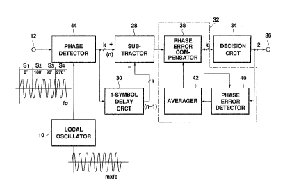
FIG. 1 shows a differentlal-detection demoduIator
clrcuit which is a quadru-phase PSK differential-
detection circuit.
In this illustrated embodiment, $he mixers 14, 18,
the phase shifter 16, the low-pass filters 20, 22, *he
AtD converter 24 and the phase angle processor 26 of the
eonventlonal art are replaeed by a phase detector 44
where a quadru-phase PSK modulated signal recelved from
the input terminal 12 is converted into k-bit phase data
(k is an integer).
FIG. 2 shows the construction of the phase
detector 44.
The phase detector 44 ineludes a shift register 46
for receiving signals from a local oscillator 10. The
local oscillator 10 has an oscillated frequeney m times
a earrier frequency f~, e.g. 8xfo . This high-frequency
slgnal is supplied to the clock input of -the sh~ft
register 46, and a signal whose frequency is dlvided
into eight conpoments by a Erequeney divider 11; namely,
the ratio of frequency divlsion is 1i8. As a result,
from the -~requency divider 11, a signal whose signal ~s
substantially equal to the carrier frequency fO i8
supplied to th0 shift input of the shif'-t register 46.
- 12 -
~L6~
Meanwhile, a quadru-phase PSK modulated signal
received from the input terminal 12 1s limited to a
predetermined voltage level by a l1miter 48 and is
supplied as a digital signal to a subsequent comparator.
The phase detector 44 includes eight digital
comparators 50-l through 50-8; the modulated signal
outputted from the limiter 48 is supplied to all of the
comparators 50, while data of di~ferent phase o-E the
shift reglster 46, i.e. el - ~8, is supplied to all of
the comparators 50. Each comparator compares the
inputted modulated signal in phase with a reference
signal and outputs the result of comparison.
These results o~ comparison are supplied to an 8
to 3 converter 52 which outputs this phase as a 3-bit
signal based on the inputted eight signals.
The operation of this embodiment will now be
described.
FIG. 3 is a timing chart showing the operatlon of
the phase detector 4~. Reference s1gnals ~ 8 are
diEferent ~rom one another by 46~. For example~ the
reference signal ~l has a phase of 22.5~; the reference
signal ~2, a phase of 67.5~; ...; and the re~erence
signal 08, a phase o~ 337.5~.
- 13 -
2~
In symbol n-l, assumirlg that a modulated slgnal
is inputted, the phase comparators 50-1, 50-2, ....
50-8 compare the respective reference signals el, e2,
..., ~8 with the modulated signal ~ . If the result
o~ comparison shows coincidence, the phase comparators
50-1, 50-2, ..., 50-8 output a slgnal of H value. I-
~the result o-f comparison shows dissidence, they output a
signal of L value.
Assumlng that the modulated signal 0~-1 has a
phase o~ 170~, for example, the output of the phase
comparator 50-1 will be an H value. Likewise, -the
output of each o~ the phase comparators 50-2, 50-3, 50-4
wlll be an H value. However, since the phase Oe the
re~erence signal ~5 supplied to the phase comparator
50-5 is 202.5~, the output of the phase comparator 50-5
will be an L value. As a result, signals to be supplied
to the 8 to 3 converter 52 will be ~I~T~TT.TT in the order
v~' phase comparators.
In the 8 to 3 converter 52, a range in which the
phase o-E the modulated signal e~ ~ exists is decided
based on the signals supplied from the phase comparators
50-1, 50-Z, ..., 50-8. In this case, partly since the
signal supplied from the phase comparator 50-4 is an H
- 14 -
6~
value and partly slnce the signal supplied from the
phase comparator 50-5 is an L value, it i.5 decided that
the phase o-f the modulated signal ~ exists within a
range O-r 157.5~ to 202.5~. The 8 to 3 converter 52
outputs, as phase data, a value representing a range of
157.5~ to 202.5~, e.g. 180~.
Slmilarly, assuming that in symbol n the modulated
si~nal e~ ls supplied, if the modulated signal e~ has a
phase of 265~, the ou-tputs of the phase comparators
50-1, 50-2, ..., 50-8 will be ~T.T.T.T.~ in order. The 8
to 3 converter 52 decides similarly to the case of
timing n-1 and outputs, as phase data, a value 270~
representing a range of 247.5~ to 292.50.
Likewi~e in the conventional art, the thus
obtained phase data is supplied to both the subtracter
28 and the 1-symbol delay circuit 30. In the subtracter
28, the phase data relating to the modulated signal
(180~) is subtracted from the phase data relating
to the modulated signal ~ so that the phase difference
s~gnal to be outputted from the subtracter 28 will be a
phase difference signal indicating 90~.
When the phase difference signal having such value
is supplied to a decision circuit 34 via a frequency
- 15 -
2~6~8~1.
error compensator 32, the decision circuit 34 makes a
decision of symbol. In thls embodiment, slnce the
predetermined relationship between the angle between two
symbols and demodulation data ls oV(0,0), 90~(1, 0~,
180~~1, 1) and 270~(0, 1), a symbol Or (I, Q)=(1, 0) is
decided.
In -this embodiment, it is possible to convert the
modulated signal into phase data using only a dlgital
means, without any analog means. In the absence of
analog elements or parts, it is easy to integrate parts
on a single semiconductor chip and also to make them
free from ad~ustment.
In addition, since this demodulator circuit unlike
the conventional demodulator circuit 24 is constructed
wlthout using an analog-to-digital converter or a phase
angle converter 26, which requires a large-capacitance
memory, lt is posslble to reduce the consumed electrical
power o~ the circuit and also to simpli~y the
construction of the circuit.
In this embodiment, the eight-phase reference
signals el - ~8 and quadru-phase PSK are used.
Alternatively, a dif~erent modulatlon method may or a
different number of phases of re~erence slgnal may he
- 16 -
6~
used. Namely, this invention can be applled to a
modulation method, besides PSK, which is differentially
detectable. Further, it is possible to improve the
aGcuracy o~ phase data by increasing the number of
phases o-f re~erence signal.
FIG. 4 shows a pre~erred phase detector according
to a second embodiment. This phase detector, like the
first embodiment, is a digital circuit.'
A quadru-phase PSK modulated signal supplied from
an input terminal 100 and having a carrier frequency fO
is limited to a predetermined voltage level by a limiter
lOl, and the resulting signal is supplied to the set
input of a -~lip-flop (FF) 102 as a digital slgnal.
FIG. 5 is a timing chart showing the operation of
the second embodlment, in which FF 102 is set by the
rising o~' the inputted modulated signal.
In the second embodiment, the phase differenca
between the inputted modulated signal and a locally
oscillated signal is counted by a counter 103. To the
~clock input of' the counter 103, count clocks m times the
carrier frequency are supplied from a clock signal
oscillator 104. To the count enable terminal (CE) of
the counter 103, Q signal B o-f FF 102 is supplied, and
- 17 -
to the reset input o* the counter 103 the output A2 of a
frequency divider 105 is supplied.
As a result, in FI~. 4, a carrier frequency signal
of the demodulator circuit is obtained by the oscillator
104 and the divider 105 and is supplied to the reset
terminal of FF 102 as a signal A1. The output B of FF
102, as shown in FIG. 5, has a pulse width from the
rising of the inputted modulated signal to the rising of
the locally oscillated signal in the demodulator
circuit. Then the counter 103 counts clocks tmxfO)
between the outputs B.
From the divider 105, a pulse signal A2 is
outputted at the same tlming as the locally oscillated
signal A1. The pulse signal A2 is then supplied to the
latch input oE a latch circuit 107 via an inverter 106.
The latch circuit 107 latches a count value o~ the
counter 103, whereupon the counter 103 is reset by the
pulse signal A2 to become prepared for the next phase
di~-ference operation.
Therefore, also in the second embodiment, the
output o-f the latch circuit 107 indicates the phase
dif~erence between the inputted modulated signa] and the
locally oscillated signal of the demodulator circuit,
- 18 -
2al46~
and this output will be used in differential-detection
as described above.
The phase comparator circuit, like the first
embodiment, is composed o~ only digital circuits and
hence can be simplified.
According to this invention, since the means for
eonverting the modulated signal is realized by a digital
means based on 2-value signals, no analog element is
requlred so that it is easy to integrate all elements or
parts o~ the circuit on a single chip and to make the
eireuit free from adJustment. Further, since no
analog-to-digital converter is required, it is possible
to realize a low electrlcal power consumption. Since no
large-capacitance memory is required, it is possible to
simplified the circuit construction.
, : ~
: ~ :
~ :
.,~ . ...