Note: Descriptions are shown in the official language in which they were submitted.
~ -~ 2046~2~
--1--
ORGANIC ELECTROLUMINESCENT DEVICE WITH
STABILIZING CATHODE CAPPING LAYER
Field of the Invention
This invention relates to organic electro-
S luminescent devices. More specifically, this inven-
tion relates to devices which emit light from a
current conducting organic layer.
Background of the Invention
Electroluminescent devices (hereinafter
also referred to as EL devices) contain spaced elec-
trodes separated by an electroluminescent medium
that emits electromagnetic radiation, typically
light, in response to the application of an electri-
cal potential difference across the electrodes. The
electroluminescent medium must not only be capable
of luminescing, but must also be capable of fabrica-
tion in a continuous form (i.e., must be pin hole
free) and must be sufficiently stable to facilitate
fabrication and to support device operation.
Initially organic EL devices were fabri-
cated using single crystals of organic materials, as
illustrated by Mehl et al U.S. Patent 3,530,325 and
Williams U.S. Patent 3,621,321. Single organic
crystal EL devices were relatively difficult to
fabricate and further did not readily lend them-
selves to thin film constructions.
In recent years preferred organic EL
devices have been constructed employing thin film
deposition techniques. Using an anode as a device
support, the organic electroluminescent medium has
been deposited as one or a combination of thin films
followed by the deposition of a cathode, also formed
as a thin film deposition. Thus, starting with the
anode structure, it is possible to form the entire
1 2046~20
~ -2-
active structure of an organic EL device by thin
film deposition techniques. As employed herein the
term ~thin film" refers to layer thicknesses of less
than 10 mm, with layer thicknesses of less than
about 5 mm being typical. Examples of organic EL
devices containing organic electroluminescent medium
and cathode constructions formed by thin film depo-
sition techniques are provided by Tang U.S. Patent
4,356,429, VanSlyke et al U.S. Patents 4,539,507 and
4,720,432, and Tang et al U.S. Patents 4,769,292 and
4,885,211.
While the art has encountered little
difficulty in constructing fully acceptable stable
anodes for internal junction organic EL devices,
cathode construction has been a matter of extended
investigation. In selecting a cathode metal, a
balance must be struck between metals having the
highest electron injecting efficiencies and those
having the highest levels of stability. The highest
electron injecting efficiencies are obtained with
alkali metals, which are too unstable for convenient
use, while metals having the highest stabilities
show limited electron injection efficiencies and
are, in fact, better suited for anode construction.
Despite improvements in the construction
of organic EL devices, a persistent problem has been
dark spot formation in environments in which the
organic EL device is exposed to some level of mois-
ture in the ambient atmosphere. Microscopic analy-
sis of organic EL devices exhibiting dark spot
behavior has revealed oxidation of the cathode
occurring at its interface with the organic electro-
luminescent medium. It is believed that the oxida-
tion of the cathode metal at its interface with the
organic electroluminescent medium creates a resis-
2 ~ 2 ~
--3--
tive barrier to current flow in affected areas ofthe organic EL device. Without current flow in an
area of the organic EL device, no electrolumines-
cence can occur, and the result is seen as a dark
S spot when other areas of organic EL device are emit-
ting.
Tang et al U.S. Patent 4,885,211 teaches
to form the cathodes of organic EL devices of a
combination of metals, with at least 50 percent
(atomic basis) of the cathode being accounted for by
a metal having a work function of less than 4.0 eV.
Tang et al in Example 3 demonstrates a 1:1 weight
ratio silver-europium electrode.
Sllmm~ry of the Invention
The present invention has as its purpose
to curtail the emergence of dark spots in organic EL
devices.
In one aspect this invention is directed
to an organic electroluminescent device comprised
of, in sequence, a support, an anode, an organic
electroluminescent medium, and a cathode containing
a plurality of metals other than alkali metals. The
device is characterized in that the cathode is
comprised of a capping layer containing at least one
alkaline earth or rare earth metal and, interposed
between the capping layer and the organic electrolu-
minescent medium, an electron injecting layer
containing at least one metal having a work function
of less than 4.0, but exhibiting a higher work
function than the alkaline earth or rare earth
metals in the capping layer.
20~62~
,
--4--
It is a further object of the invention to
provide an organic EL device having improved cathode
characteristics that is compatible with formation by
thin film deposition techniques.
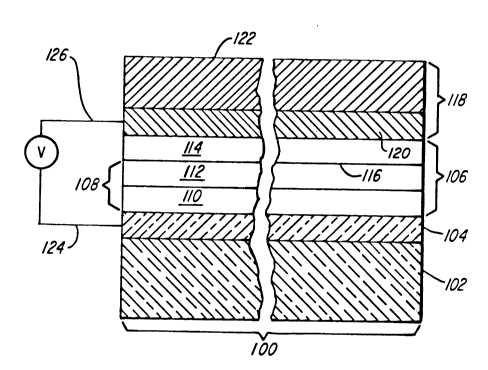
S Brief DescriDtion of the Drawin~s
Figure 1 is schematic diagram of an
organic EL device according to the invention.
The drawings are necessarily of a
schematic nature, since the thicknesses of the indi-
vidual layers are too thin and thickness differencesof the various elements are too greater to permit
depiction to scale or to permit convenient propor-
tionate scaling.
DescriDtion of Preferred ~mhodiments
An organic electroluminescent (EL) device
100 is shown in Figure 1 consisting of a light
transmissive support 102 onto which is coated a
light transmissive anode 104. Overlying the anode
is an organic electroluminescent medium 106. As
shown, the organic electroluminescent medium is
divided into (1) a hole injecting and transporting
zone 108, which is further divided into (a) a hole
injecting layer 110 contacting the anode and (b) an
overlying hole transporting layer 112, and (2) an
electron injecting and transporting zone 114 forming
a junction 116 with the hole transporting layer.
A cathode 118 consisting of an electron
injecting layer 120 and a capping layer 122 overlies
the organic electroluminescent medium. The electron
injecting layer forms an interface with the electron
injecting and transporting zone of the organic
electroluminescent medium.
20~622û
_,.
--5--
In use the anode 104 and cathode 118 are
connected to an external power source V by conduc-
tors 124 and 126, respectively. The power source
can be a continuous direct current or alternating
S current voltage source or an intermittent current
voltage source. Any convenient conventional power
source, including any desired switching circuitry,
can be employed which is capable of positively bias-
ing the anode with respect to the cathode. Either
the anode or cathode can be at ground potential.
The organic EL device can be viewed as a
diode which is forward biased when the anode is at a
higher potential than the cathode. Under these
conditions injection of holes occurs from the anode
into the hole injecting layer 110 of the hole
injecting and transporting zone 106. The holes are
transported across the hole transporting layer 112
and across the junction 116 into the electron
injecting and transporting zone 114. Concurrently
electrons are injected from the cathode 118 into the
electron injecting and transporting zone 114. When
a migrating electron drops from its conduction band
potential to a valence band in filling a hole,
energy is released as light. Depending upon the
choice of alternative constructions, the released
light can be emitted from the organic electrolumi-
nescent medium through one or more edges of the
organic electroluminescent medium separating the
electrodes, through the anode and support, through
the cathode, or through any combination of the fore-
going. Since the organic electroluminescent medium
is quite thin, it is usually preferred to emit light
through one of the two electrodes. In the preferred
form of the EL device shown the anode and support
are specifically constructed to be light transmis-
20~622~
_,
--6--
sive, thereby facilitating emission through theseelements.
Reverse biasing of the electrodes reverses
the direction of mobile charge migration, depletes
the organic electroluminescent medium of mobile
charge carriers, and terminates light emission.
When an AC power source is employed, the internal
junction organic EL devices are forward biased
during a portion of each period and reverse biased
during the remaining portion of the period.
To allow the organic EL device to operate
efficiently the cathode must contain at least one
metal having a relative low (less than 4.0 eV) work
function in contact with the organic electrolumines-
cent medium. Therefore, the lowest work functionmetal present in the cathode at the interface is
particularly susceptible to oxidation. The presence
of moisture in the ambient atmosphere surrounding
the organic EL device has been observed to lead to
oxidation of the cathode low work function metal at
its interface with the organic electroluminescent
medium, even when a low work function metal is
present in only a limited amount or is overcoated
with a higher work function metal. While the
susceptibility of the cathode to oxidation is inher-
ent in the materials and operation of the cathode of
an efficient organic EL device, there are additional
contributing factors. In constructing organic EL
devices by thin film forming techniques, microchan-
nels (microscopic local disruptions) are believed tobe present in the cathodes that allow moisture
migration through the cathode to its interface with
the organic electroluminescent medium.
The present invention is based on the
discovery of a cathode construction for an organic
~0~622~
-
--7--
EL device which achieves both high levels of
efficiency and improved uniformity of light emission
from an organic EL device in the presence of ambient
moisture--i.e., curtailed dark spot emergence over
time.
The high levels of efficiency are achieved
by employing a cathode electron injecting layer that
contains a mixture of metals, at least one of which
has a low (<4.0 eV) work function (but excluding, of
course, the alkali metals, which are too unstable
for convenient use). In this respect the invention
is implementing the teachings of Tang et al U.S.
Patent 4,885,211, cited above, but with the very
significant difference that the low work function
metal need not form more than a minor amount of the
electron injecting layer of the cathode. Preferred
cathode electron injecting layers contain at least
0.05 percent (optimally at least 0.10 percent) of
the low work function metal. (As herein employed
all percentages are weight percentages based on
total weight, unless otherwise indicated.) The high
(>4.0 eV) work function metal or metals in the
cathode electron injecting layer can be employed in
any convenient concentration. Deposition benefits
can be realized when the high work function metal
accounts for as little as 1 percent of the cathode
electron injecting layer, with high work function
metal concentrations in this layer preferably being
at least 2 percent. The high work function metal
can account for the entire content of the electron
injecting layer not provided for by the low work
function metal, with high work function metal
concentrations of in excess of 80 percent and even
in excess of 90 percent being specifically contem-
3s plated.
20~622J
To improve the uniformity of light emis-
sion in the presence of ambient moisture the cathode
is provided with a capping layer. Capping layers of
aluminum, which has a work function of about 4.25
eV, have been demonstrated to be ineffective in
curtailing dark spot formation. Similarly, capping
layers of organic materials, such as those used to
form the organic electroluminescent medium, have
also been demonstrated to be ineffective in curtail-
ing dark spot formation.
Quite surprisingly, it has been discoveredthat a cathode construction having a capping layer
that contains an alkaline earth and/or rare earth
metal employed in combination with an electron
injecting layer which contains at least one metal
having a low (<4.0 eV) work function, but a higher
work function than the lowest work function metal in
the capping layer--i.e., a lower function than the
alkaline earth and/or rare earth metal in the cap-
ping layer, protects the organic EL device from darkspot emergence ! in the presence of moisture. It is
surprising that adding to the cathode construction
one or more metals having a lower work function than
the lowest work function metal in the electron
injecting layer of the cathode enhances device
stability. Since alkaline earth and rare earth
metals have work functions that are intermediate
between metals commonly employed in cathode
construction and, in most instances, the work func-
tions of alkali metals, it would be reasonable toconclude that the addition of alkaline earth and/or
rare earth metals to cathode construction would
degrade device stability.
It is believed that the cathode capping
layers containing at least one alkaline earth or
20~6229
-
g
rare earth are effective to curtail dark spot forma-
tion beca~se it is oxidation at the interface of the
cathode electron injecting layer and the organic
electroluminescent medium that is primarily respon-
sible for dark spot emergence, rather than oxidationof portions of the cathode removed spatially remote
from this interface. By confining the alkaline
earth or rare earth metal to a capping layer out of
direct contact with the organic electroluminescent
medium, the alkaline earth or rare earth metal is
located to intercept and react with moisture that
would otherwise reach the interface of the cathode
and the organic electroluminescent medium. Oxida-
tion of the alkaline earth or rare earth metal does
not degrade device efficiency, since it is the
lowest work function metal in contact with the
organic electroluminescent medium that controls
device efficiency. Similarly, oxidation of the
alkaline earth or rare earth metal does not promote
dark spots, since the site of oxidation is removed
from the electron injecting interface with the
organic electroluminescent medium.
To be effective in curtailing dark spot
formation the capping layer is at least 500A
(preferably at least lo00A and optimally at least
2000A) in thickness. Any convenient capping layer
thickness can be employed. For example, using thin
film deposition techniques, capping layer thick-
nesses of up to about 20 ~m can be readily formed.
Generally the full advantages of the invention are
realized with capping layer thicknesses of at least
5 ~m, with maximum fused metal particle layer thick-
nesses of about 2 ~m being preferred.
The foregoing capping layer thicknesses
are predicated on the assumption of one or a combi-
-lo- 2046220
nation of alkaline earth and rare earth metals
accounting for at least 80 percent and optimally at
least 90 percent of the capping layer. It is generally
preferred that the capping layer consist essentially of
one or a combination of alkaline earth and rare earth
metals. However, it is recognized that the presence of
one or more other metals in minor amounts may be
advantageous to facilitate formation of smooth capping
layers, depending upon the layer formation technique
employed.
In one specifically preferred form the
electron injecting layer of the cathode can be
identical to any of the cathodes satisfying the
requirements of Tang et al U.S. Patent 4,885,211.
Specifically, the Mg:Ag cathodes of Tang et al U.S.
Patent 4,885,211 constitute one preferred electron
injecting cathode layer construction, but the magnesium
can be present in the ranges noted above rather than in
concentrations of greater than 50 percent, as suggested
by Tang et al.
In another preferred form the cathode
electron injecting layer can be comprised of aluminum
and magnesium.
In the foregoing preferred cathode
electron injecting layer constructions magnesium is
employed, but it is recognized that other metals in the
work function range of 3.9 eV to 3.5 eV can be
substituted. Among metals in this work function range
beryllium, manganese, gallium, indium, hafnium and
thallium, are specifically preferred. Any one or
combination of these metals can be substituted
20~6~2~
--11--
for or employed incombination with magnesium.
The cathode capping layer can be formed of
any convenient alkaline earth or rare earth metal or
combination of these metals, provided that any metal
so chosen has a work function less than that of any
metal in the cathode electron injecting layer. For
example, when the the lowest work function metal is
in the range of from 4.0 eV to 3.5 eV, any rare
earth metal can be present in the capping layer,
since all rare earth metals having a work function
of less than 3.5 eV. As employed herein, the term
"rare earth" refers to the Group 3 metals scandium,
yttrium and the lanthanide series of elements.
All of the alkaline earth metals have a
work function of less than 3.0 eV, except beryllium
and magnesium. It is therefore apparent that beryl-
lium or magnesium can be employed either in the
electron injecting layer or in the capping layer,
depending on the other metal or metals to employed
in combination. However, since beryllium has a work
function of 3.9 eV, there are relatively few metals
having a higher work function, but still less than
4.0 eV that can employed in combination to allow the
beryllium to be located in the capping layer. On
the other hand, the preferred Mg containing electron
injecting layers noted above can be employed in
combination with a capping layer containing any
alkaline earth and/or rare earth metal, provided
that at least one of the alkaline earth and rare
earth metals is not magnesium. Conversely, when the
electron injecting layer contains as its lowest work
function element a metal, such as indium, gallium or
indium, having a higher work function than magne-
sium, the advantages of the invention can be real-
ized by employing magnesium in the capping layer.
20~622~
-
-12-
The rare earth elements can be divided
into two categories: (1) those having a work func-
tion in the range of from 3.0 to 3.5 eV, such as
scandium, yttrium, lanthanum neodymium, samarium,
S gadolinium, terbium, dysprosium, erbium, holmium,
thulium and lutetium, and (2) those having a work
function in the range of from 2.5 to 3.0 eV, such as
cerium, praseodymium, europium and ytterbium. It is
possible to locate the rare earths in category (1)
in the cathode injecting layer while locating the
rare earths in category (2) in the capping layer.
It is apparent that still other combina-
tions are possible by choosing the lowest work func-
tion metal to be located in the capping layer and
ano~her, higher work function metal, but one having
a work function of less than 4.0 eV, to be present
in the cathode injecting layer.
The anode of the organic EL device can
take any convenient conventional form. Typically
the anode is constructed of one or a combination of
metals having a work function in excess of 4.0 eV.
Metals having work functions >4.0 eV are listed by
Tang et al U.S. Patent 4,885,211. When, as is
preferred, luminescence is intended to occur through
the anode, it is preferred to construct the anode of
one or a combination of light transmissive metal
oxides, such as indium oxide, tin oxide or, opti-
mally, indium tin oxide (ITO).
2 0 ~. 6 ~ 2 ~
-
-13-
As employed herein the term ~light trans-
missive~ means simply that the layer or element
under discussion transmits greater than 50 percent
of the light of at least one wavelength it receives
and preferably over at least a 100 nm interval.
Since both specular (unscattered) and diffused
(scattered) emitted light are desirable device
outputs, both translucent and transparent (or
substantially transparent) materials are useful. In
most instances the light transmissive layers or
elements of the organic EL device are also colorless
or of neutral optical density--that is, exhibit no
markedly higher absorption of light in one wave-
length range as compared to another. However, it
is, of course, recognized that light transmissive
electrode supports or separate superimposed films or
elements can be tailored in their light absorption
properties to act as emission trimming filters, if
desired. Such an electrode construction is
disclosed, for example, by Fleming U.S. Patent
4,035,686. The light transmissive conductive layers
of the electrodes, where fabricated of thicknesses
approximating the wavelengths or multiples of the
light wavelengths received can act as interference
filters.
The organic electroluminescent medium can
be chosen from any one or combination of the organic
materials taught to form the organic electrolumines-
cent medium of the organic EL devices disclosed by
Tang U.S. Patent 4,356,429, VanSlyke et al U.S.
Patent 4,539,507, Tang et al U.S. Patent 4,769,292
and 4,885,211. Although the most advantageous
constructions are those that employ the zones and
layers described above in connection device 100, the
organic electroluminescent medium can be a unitary
20~L6~2~
-
-14-
layer.
To achieve high levels of organic EL
device efficiency it is contemplated to construct
the organic electroluminescent medium of at least
S two different zones, an electron injecting and
transporting zone, which is typically a single
layer, and a hole injecting and transporting zone.
The hole injecting and transporting zone can be
constructed also of a single layer, but it is most
efficiently constructed of a hole injecting layer
and a hole transporting layer.
In a preferred form of the invention a
layer containing a porphyrinic compound forms the
hole injecting layer of the internal junction
organic EL device. A porphyrinic compound is any
compound, natural or synthetic, which is derived
from or includes the porphyrin structure. Any of
the porphyrinic compounds disclosed by Adler U.S.
Patent 3,935,031 or Tang U.S. Patent 4,356,429 can
be employed.
Preferred porphyrinic compounds are those
of structural formula (I):
(I) T2 T
T
wherein
Q is -N= or -C(R)=;
2046~2~
-15-
M is a metal, metal oxide, or metal halide;
R is hydrogen, alkyl, aralkyl, aryl, or
alkaryl, and
Tl and T2 represent hydrogen or together
S complete a unsaturated 6 membered ring, which can
include substituents, such as alkyl or halogen.
Preferred alkyl moieties contain from about 1 to 6
carbon atoms while phenyl constitutes a preferred
aryl moiety.
In an alternative preferred form the
porphyrinic compounds differ from those of struc-
tural formula (I) by substitution of two hydrogen
for the metal atom, as indicated by formula (II):
(II)
T 2~T 2
T T2
Highly preferred examples of useful
porphyrinic compounds are metal free phthalocyanines
and metal containing phthalocyanines. While the
porphyrinic compounds in general and the phthalocya-
~0 nines in particular can contain any metal, the metal
preferably has a positive valence of two or higher.
Exemplary preferred metals are cobalt, magnesium,
zinc, palladium, nickel, and, particularly, copper,
lead, and platinum.
Illustrative of useful porphyrinic
compounds are the following:
~0~22~ ~
-16-
PC-l Porphine
PC-2 1,10,15,20-Tetraphenyl-21H,23H-porphine
copper (II)
PC-3 1,10,15,20-Tetraphenyl-21H,23H--porphine
S zinc (II)
PC-4 5,10,15,20-Tetrakis(pentafluorophenyl)-
21H,23H-porphine
PC-5 Silicon phthalocyanine oxide
PC-6 Aluminum phthalocyanine chloride
PC-7 Phthalocyanine (metal free)
PC-8 Dilithium phthalocyanine
PC-9 Copper tetramethylphthalocyanine
PC-10 Copper phthalocyanine
PC-ll Chromium phthalocyanine fluoride
PC-12 Zinc phthalocyanine
PC-13 Lead phthalocyanine
PC-14 Titanium phthalocyanine oxide
PC-15 Magnesium phthalocyanine
PC-16 Copper octamethylphthalocyanine
The hole transporting layer of the organic
EL device contains at least one hole transporting
aromatic tertiary amine, where the latter is under-
stood to be a compound containing at least one
trivalent nitrogen atom that is bonded only to
2s carbon atoms, at least one of which is a member of
an aromatic ring. In one form the aromatic tertiary
amine can be an arylamine, such as a monoarylamine,
diarylamine, triarylamine, or a polymeric arylamine.
Exemplary monomeric triarylamines are illustrated by
Klupfel et al U.S. Patent 3,180,730. Other suitable
triarylamines substituted with vinyl or vinylene
radicals and/or containing at least one active
hydrogen containing group are disclosed by Brantley
et al U.S. Patents 3,567,450 and 3,658,520.
A preferred class of aromatic tertiary
20~622~
amines are those which include at least two aromatic
tertiary amine moieties. Such compounds include
those represented by structural formula (III):
(III)
Ql Q2
G
wherein
Ql and Q2 are independently aromatic tertiary
amine moieties and
G is a linking group such an arylene,
cycloalkylene, or alkylene group or a carbon to
carbon bond.
A particularly preferred class of triary-
lamines satisfying structural formula (III) and
containing two triarylamine moieties are those
satisfying structural formula (IV):
(IV)
R2
Rl- C - R3
R4
where
Rl and R2 each independently represents a
hydrogen atom, an aryl group or alkyl group or
and R2 together represent the atoms completing a
cycloalkyl group and
. R3 and R4 each independently represents an aryl
group which is in turn substituted with a diaryl
substituted amino group, as indicated by structural
formula (V):
204~2~
-18-
(V)
R5
- N
R6
wherein R5 and R6 are independently selected aryl
groups.
Another preferred class of aromatic
tertiary amines are tetraaryldiamines. Preferred
tetraaryldiamines include two diarylamino groups,
such as indicated by formula (V), linked through an
arylene group. Preferred tetraaryldiamines include
those represented by formula (VI).
15 (VI)
R7 R8
N - Aren - N
Ar R9
wherein
Are is an arylene group,
n is an integer of from l to 4, and
Ar, R , R8, and R9 are independently
selected aryl groups.
The various alkyl, alkylene, aryl, and
arylene moieties of the foregoing structural formu-
lae (III), (IV), (V), and (VI) can each in turn be
substituted. Typical substituents including alkyl
-30 groups, alkoxy groups, aryl groups, aryloxy groups,
and halogen such as fluoride, chloride, and bromide.
The various alkyl and alkylene moieties typically
contain from about l to 5 carbon atoms. The
cycloalkyl moieties can contain from 3 to about lO
carbon atoms, but typically contain five, six, or
seven ring carbon atoms--e.g., cyclopentyl, cyclo-
2Q4622~;
--19--
hexyl, and cycloheptyl ring structures. The aryland arylene moieties are preferably phenyl and
phenylene moieties.
Representative useful aromatic tertiary
amines are disclosed by Berwick et al U.S. Patent
4,175,960 and Van Slyke et al U.S. Patent 4,539,507.
Berwick et al in addition discloses as useful hole
transporting compounds N substituted carbazoles,
which can be viewed as ring bridged variants of the
diaryl and triarylamines disclosed above.
Following the teachings of VanSlyke et al
(II), cited above, it is possible to achieve higher
organic EL device stabilities both during short term
and extended operation by substituting for one or
more of the aryl groups attached directly to a
tertiary nitrogen atom in the aromatic tertiary
amines described above an aromatic moiety containing
at least two fused aromatic rings. The best combi-
nation of both short term (0-50 hours) and long term
(0-300+ hours) of operation are achieved when the
aromatic tertiary amines are those which (1) are
comprised of at least two tertiary amine moieties
and (2) include attached to a tertiary amine nitro-
gen atom an aromatic moiety containing at least two
fused aromatic rings. The following is a listing of
exemplary aromatic compounds containing at least two
fused aromatic rings and from 10 to 24 ring carbon
atoms:
Naphthalene,
Azulene,
Heptalene,
~-Indacene,
s-Indacene,
Acenaphthylene,
Phenalene,
2046~20
-20-
Phenanthrene,
Anthracene,
Fluoranthrene,
Acephenathrylene,
s Aceantrylene,
Triphenylene,
Pyrene,
Chrysene,
Naphthacene,
Pleiadene,
Picene,
Perylene,
Pentaphene,
Hexaphene,
Rubicene, and
Coronene.
The fused aromatic ring moieties of the tertiary
amines preferably contain from about 10 to 16 ring
carbon atoms. While unsaturated 5 and 7 membered
rings can be fused to six membered aromatic rings
(i.e., benzene rings) to form useful fused aromatic
ring moieties, it is generally preferred that the
fused aromatic ring moiety include at least two
fused benzene rings. The simplest form of a fused
aromatic ring moiety containing two fused benzene
rings is naphthalene. Therefore, the preferred
aromatic ring moieties are naphthalene moieties,
where the latter is understood to embrace all
compounds containing a naphthalene ring structure.
In monovalent form the naphthalene moieties are
naphthyl moieties, and in their divalent form the
naphthalene moieties are naphthylene moieties.
Illustrative of useful aromatic tertiary
amines are the following:
` 20~22~3
_. .
-21-
ATA-1 1,1-Bis(4-di-p-tolylaminophenyl)-
cyclohexane
ATA-2 1,1-Bis(4-di-p-tolylaminophenyl)-4-
phenylcyclohexane
S ATA-3 4,4'-Bis(diphenylamino)quadriphenyl
ATA-4 Bis(4-dimethylamino-2-methylphenyl)-
phenylmethane
ATA-5 N,N,N-Tri(p-tolyl)amine
ATA-6 4-(di-p-tolylamino)-4'-[4(di-p-tolyl-
amino)styryl]stilbene
ATA-7 N,N,N',N'-Tetra-p-tolyl-4,4'-diamino-
biphenyl
ATA-8 N,N,N',N'-Tetraphenyl-4,4'-diamino-
biphenyl
ATA-9 N-Phenylcarbazole
ATA-10 Poly(N-vinylcarbazole)
ATA-11 4,4'-Bis[N-(1-naphthyl)-N-phenyl-
amino]-biphenyl
ATA-12 4,4~-Bis[N-(1-naphthyl)-N-phenyl-
amino]-p-terphenyl
ATA-13 4,4'-Bis[N-(2-naphthyl)-N-phenyl-
amino]biphenyl
ATA-14 4,4'-Bis[N-(3-acenaphthenyl)-N-
phenylamino]biphenyl
ATA-15 1,5-Bis[N-(1-naphthyl)-N-phenyl-
amino]naphthalene
ATA-16 4,4'-Bis[N-(9-anthryl)-N-phenyl-
amino]biphenyl
. ATA-17 4,4~-Bis[N-(1-anthryl)-N-phenyl-
amino]-p-terphenyl
ATA-18 4,4'-Bis[N-(2-phenanthryl)-N-phenyl-
amino]biphenyl
ATA-19 4,4'-Bis[N-(8-fluoranthenyl)-N-
phenylamino]biphenyl
ATA-20 4,4'-Bis[N-(2-pyrenyl)-N-phenyl-
2~622~
amino]biphenyl
ATA-21 4,4'-Bis[N-(2-naphthacenyl)-N-phenyl-
amino]biphenyl
ATA-22 4,4'-Bis[N-(2-perylenyl)-N-phenyl-
amino]biphenyl
ATA-23 4,4'-Bis[N-(1-coronenyl)-N-phenyl-
amino]biphenyl
ATA-24 2,6-Bis(di-~-tolylamino)naphthalene
ATA-25 2,6-Bis[di-(1-naphthyl)amino]naph-
thalene
ATA-26 2,6-Bis[N-(1-naphthyl)-N-(2-naph-
thyl)amino]naphthalene
ATA-27 4,4~-Bis[N,N-di(2-naphthyl)amino]-
terphenyl
ATA-28 4,4'-Bis{N-phenyl-N-[4-(1-naphthyl)-
phenyl]amino}biphenyl
ATA-29 4,4'-Bis[N-phenyl-N-(2-pyrenyl)-
amino]biphenyl
ATA-30 2,6-Bis[N,N-di(2-naphthyl)-
amine]fluorene
ATA-31 4,4~-Bis(N,N-di-p-tolylamino)-
terphenyl
ATA-32 Bis(N-1-naphthyl)(N-2-naphthyl)amine
Any conventional electron injecting and
transporting compound or compounds can be employed
in forming the layer of the organic electrolumines-
cent medium adjacent the cathode. This layer can be
formed by historically taught electroluminescent
materials, such as anthracene, naphthalene, phenan-
threne, pyrene, chrysene, and perylene and otherfused ring luminescent materials containing up to
about 8 fused rings as illustrated by Gurnee et al
U.S. Patent 3,172,862, Gurnee U.S. Patent 3,173,050,
Dresner, ~Double Injection Electroluminescence in
Anthracene", RCA Review, Vol. 30, pp. 322-334, 1969;
20~622~
-23-
and Dresner U.S. Patent 3,710,167.
Among electron injecting and transporting
zone compounds useful in forming thin films are the
butadienes, such as 1,4-diphenylbutadiene and
S tetraphenylbutadiene; coumarins; and stilbenes, such
as trans-stilbene, disclosed by Tang U.S. Patent
4,356,429, cited above.
Still other thin film forming electron
injecting and transporting zone compounds which can
be used to form the layer adjacent the cathode are
optical brighteners, particularly those disclosed by
VanSlyke et al U.S. Patent 4,539,507, cited above.
Useful optical brighteners include those satisfying
structural formulae (VII) and (VIII):
(VII)
R~Cz ~R4
or
(VIII)
R 1 ~>_
wherein
R1, R2, R3, and R4 are individually hydro-
gen; saturated aliphatic of from 1 to 10 carbon
atoms, for example, propyl, t-butyl, heptyl, and the
like; aryl of from 6 to 10 carbon atoms, for exam-
ple, phenyl and naphthyl; or halo such as chloro,
fluoro, and the like; or R1 and R2 or R3 and R4
taken together comprise the atoms necessary to
2 Q ~
-24-
complete a fused aromatic ring optionally bearing at
least one saturated aliphatic of from l to lO carbon
atoms, such as methyl, ethyl, propyl and the like;
R5 is a saturated aliphatic of from l to
20 carbon atoms, such as methyl, ethyl, n-eicosyl,
and the like; aryl of from 6 to lO carbon atoms, for
example, phenyl and naphthyl; carboxyl; hydrogen;
cyano; or halo, for example, chloro, fluoro and the
like; provided that in formula (VII) at least two of
R3, R4 and R5 are saturated aliphatic of from 3 to
lO carbon atoms, e.g., propyl, butyl, heptyl and the
like;
Z is -O-, -NH-, or -S-; and
Y is
-R6-(CH=CH-)R6-,
_
- ~ m
, -CH=CH-,
-(CH=CH-)R6-(CH=CH-) n~ '
~/ ' Z "
or
~S~
wherein
m is an integer of from 0 to 4;
n is arylene of from 6 to lO carbon atoms,
for example, phenylene and naphthylene; and
Z' and Z" are individually N or CH.
As used herein ~aliphatic~ includes substituted
2046~2~
-25-
aliphatic as well as unsubstituted aliphatic. The
substituents in the case of substituted aliphatic
include alkyl of from 1 to 5 carbon atoms, for exam-
ple, methyl, ethyl, propyl and the like; aryl of
from 6 to 10 carbon atoms, for example, phenyl and
naphthyl; halo, such as chloro, fluoro and the like;
nitro; and alkoxy having 1 to 5 carbon atoms, for
example, methoxy, ethoxy, propoxy, and the like.
Still other optical brighteners that are
contemplated to be useful are listed in Vol. 5 of
Chemistry of Synthetic Dyes, 1971, pages 618-637 and
640. Those that are not already thin-film-forming
can be rendered so by attaching an aliphatic moiety
to one or both end rings.
Particularly preferred for use in forming
the electron injecting and transporting layers of
the organic EL devices of this inventions are metal
chelated oxinoid compounds, including chelates of
oxine (also commonly referred to as 8-quinolinol or
8-hydroxyquinoline). Such compounds exhibit both
high levels of performance and are readily fabri-
cated in the form of thin films. Exemplary of
contemplated oxinoid compounds are those satisfying
structural formula (IX):
(IX)
~------N ,----- N
Z~ ~M e+n Z~ ~M e+n
O '------ O
~ n - ~ n
wherein
Me represents a metal;
n is an integer of from 1 to 3; and
Z independently in each occurrence represents
the atoms completing a nucleus having at least two
204622~
-26-
fused aromatic rings.
From the foregoing it is apparent that the
metal can be monovalent, divalent, or trivalent
metal. The metal can, for example, be an alkali
S metal, such as lithium, sodium, or potassium; an
alkaline earth metal, such as magnesium or calcium;
or an earth metal, such as boron or aluminum.
Generally any monovalent, divalent, or trivalent
metal known to be a useful chelating metal can be
employed.
Z completes a heterocyclic nucleus
containing at least two fused aromatic rings, at one
of which is an azole or azine ring. Additional
rings, including both aliphatic and aromatic rings,
can be fused with the two required rings, if
required. To avoid adding molecular bulk without
improving on function the number of ring atoms is
preferably maintained at 18 or less.
Illustrative of useful chelated oxinoid
compounds are the following:
C0-1 Aluminum trisoxine
[a.k.a., tris(8-quinolinol) aluminum]
C0-2 Magnesium bisoxine
[a.k.a., bis(8-quinolinol) magnesium]
C0-3 Bis[benzo{f}-8-quinolinol] zinc
C0-4 Aluminum tris(5-methyloxine)
[a.k.a., tris(5-methyl-8-quinolinol)-
aluminum]
C0-5 Indium trisoxine
[a.k.a., tris(8-quinolinol) indium]
C0-6 Lithium oxine
[a.k.a., 8-quinolinol lithium]
C0-7 Gallium tris(5-chlorooxine)
[a.k.a, tris(5-chloro-8--quinolinol)
gallium]
20~62~0
-27-
C0-8 Calcium bis(5-chlorooxine)
[a.k.a, bis(5-chloro-8-quinolinol)
calcium]
CO-g Poly[zinc (II)-bis(8-hydroxy-5-quino-
s linyl)methane]
CO-10 Dilithium epindolidione
In the organic EL devices of the invention
it is possible to maintain a current density compat-
ible with efficient light emission while employing a
relatively low voltage across the electrodes by
limiting the total thickness of the organic lumines-
cent medium to less than 1 ~m (10,000 Angstroms).
At a thickness of less than 1 ~m an applied voltage
of 20 volts results in a field potential of greater
lS than 2 X 10⁵ volts/cm, which is compatible with
efficient light emission. An order of magnitude
reduction (to 0.1 ~m or 1000 Angstroms) in thickness
of the organic luminescent medium, allowing further
reductions in applied voltage and/or increase in the
field potential and hence current density, are well
within device construction capabilities.
One function which the organic luminescent
medium performs is to provide a dielectric barrier
to prevent shorting of the electrodes on electrical
biasing of the organic EL device. Even a single pin
hole extending through the organic electrolumines-
cent medium will allow shorting to occur. Unlike
conventional organic EL devices employing a single
highly crystalline luminescent material, such as
anthracene, for example, the EL devices of this
invention are capable of fabrication at very low
overall organic luminescent medium thicknesses with-
out shorting. One reason is that the presence of
three superimposed layers greatly reduces the chance
of pin holes in the layers being aligned to provide
20462~a
-28-
a continuous conduction path between the electrodes.
This in itself permits one or even two of the layers
of the organic luminescent medium to be formed of
materials which are not ideally suited for film
formation on coating while still achieving accept-
able EL device performance and reliability.
The preferred materials for forming the
organic electroluminescent medium are each capable
of fabrication in the form of a thin film--that is,
capable of being fabricated as a continuous layer
having a thickness of less than 0.5 mm or 5000
Angstroms.
When one or more of the layers of the
organic luminescent medium are solvent coated, a
film forming polymeric binder can be conveniently
co-deposited with the active material to assure a
continuous layer free of structural defects, such as
pin holes. If employed, a binder must, of course,
itself exhibit a high dielectric strength, prefer-
ably at least about 2 X 10⁶ volt/cm. Suitablepolymers can be chosen from a wide variety of known
solvent cast addition and condensation polymers.
Illustrative of suitable addition polymers are poly-
mers and copolymers (including terpolymers) of
styrene, t-butylstyrene, N-vinyl carbazole, vinyl-
toluene, methyl methacrylate, methyl acrylate, acry-
lonitrile, and vinyl acetate. Illustrative of suit-
able condensation polymers are polyesters, polycar-
bonates, polyimides, and polysulfones. To avoid
unnecessary dilution of the active material binders
are preferably limited to less than 50 percent by
weight, based on the total weight of the material
forming the layer.
The preferred active materials forming the
organic electroluminescent medium are both film
20~62~û ~
-
-29-
forming materials and capable of vacuum vapor depo-
sition. Extremely thin defect free continuous
layers can be formed by vacuum vapor deposition.
Specifically, individual layer thicknesses as low as
S about 50 Angstroms can be present while still real-
izing satisfactory EL device performance. Employing
a vacuum vapor deposited porphorinic compound as a
hole injecting layer, a film forming aromatic
tertiary amine as a hole transporting layer, and a
chelated oxinoid compound as an electron injecting
and transporting layer, thicknesses in the range of
from about 50 to 5000 Angstroms are contemplated,
with layer thicknesses in the range of from 100 to
2000 Angstroms being preferred. It is generally
preferred that the overall thickness of the organic
luminescent medium be at least about 1000 Angstroms.
ExamDles
The invention and its advantages are
further illustrated by the specific examples which
follow. The term ~atomic percent~ indicates the
percentage of a particular metal present, based on
the total number of metal atoms present. In other
words, it is analogous to mole percent, but is based
on atoms rather than molecules. The term ~cell~ as
employed in the examples denotes an organic EL
device. Examples with a number bearing the suffix E
represent embodiments of the invention while Exam-
ples with a number bearing the suffix C are included
for the purpose of comparing variations.
~ le 1C Aluminum CaDDing T~yer
An organic EL device containing a three
layer organic luminescent medium was constructed in
the following manner:
a) A transparent anode of indium tin oxide
20~62~0
--30--
coated glass was polished with 0.05 ~m alumina abra-
sive for a few minutes, followed by ultrasonic clean-
ing in a l:l (volume) mixture of isopropyl alcohol and
distilled water. It was rinsed with isopropyl alcohol
and then immersed in toluene vapor for about 5
minutes.
b) A hole injecting PC-l0 (3soA) layer was
deposited on the anode by vacuum deposition. PC-l0
was evaporated from a quartz boat using a tungsten
filament.
c) A hole transporting ATA-l (350A) layer was
then deposited on top of the PC-l0 layer. ATA-l was
also evaporated from a quartz boat using a tungsten
filament.
d) An electron injecting and transporting CO-l
(600A) layer was then deposited on top of the ATA-l
layer. CO-l was also evaporated from a quartz boat
using a tungsten filament.
e) On top of the CO-l layer was deposited a
cathode, consisting of a 2soA electron injecting
layer formed of a l0:l volume ratio of Mg and Al and a
200 oA Al capping layer.
The cell was encapsulated by placing a glass
cover over the cathode and applying Norland 60TM opti-
cal adhesive around the periphery of the cell, therebybonding the glass support bearing the anode to the
glass cover. When operated immediately following
fabrication the cell exhibited no dark spots--i.e.,
light emission was uniform over the entire anode
surface. After 70 days of storage under ambient labo-
ratory conditions (at or near standard temperature and
pressure, with humidity varying with weather condi-
tions), operation of the cell revealed that about 25
percent of the total area over which light was
initially emitted was occupied by dark spots.
20~16220
~x~m~le 2C Organic Protective T.~yer
Example lC was repeated, except that a 2000A
protective layer of CO-l was vacuum vapor deposited
over the cathode prior to encapsulating the cell.
S After 70 days of storage under identical conditions as
in Example lC approximately the same percentage of the
initial emitting area was occupied by dark spots as in
Example lC. This showed the organic material CO-l to
be ineffective in itself to reduce dark spot forma-
tion.
~x~m~le 3C Increased Thickness Aluminllm
CaDDing T.~yer
Example lC was repeated, except that anadditional 2000A of aluminum was vacuum vapor
deposited over the cathode prior to encapsulating the
cell. In other words, a total of 4000 A aluminum was
deposited over the Mg:Al electron injecting layer.
After 70 days of storage under identical conditions as
in Example lC approximately the same percentage of the
initial emitting area was occupied by dark spots as in
Example lC. This showed the additional aluminum to be
ineffective in itself to reduce dark spot formation.
~x~m~le 4C Alllm;nllm CaDDing Layer Overcoate~
with Oraanic Protective Tayer
Example lC was repeated, except that a loooA
protective layer of aluminum was vacuum vapor
deposited on the cathode (for a total of 3000A
aluminum including the capping layer) followed by the
vacuum vapor deposition of a 1000 A protective layer
of CO-l prior to encapsulating the cell. After 70
days of storage under identical conditions as in Exam-
ple lC approximately the same percentage of the
initial emitting area was occupied by dark spots as in
Example lC. This showed a superimposed combination of
20~622~
-32-
a metal protective layer and an organic material
protective layer to be ineffective to reduce dark spot
formation.
~m~le 5C No C~Dping T~yer
A cell was constructed identically as in
Example lC, except that no aluminum capping layer was
formed over the Mg:Ag electron injecting layer of the
cathode. Operation of the cell immediately following
fabrication revealed no dark spots. When the cell was
operated after being stored for 300 hours at 75C and
45% relative humidity, 38. 5% of the initially emitting
surface area of the cell was found to be occupied by
dark spots.
~xamDle 6~ ~lcillm CaDDing T~yer
lS A cell was constructed and tested identi-
cally as in Example 5C, except that a 2000A calcium
cathode capping layer was vacuum vapor deposited over
the cathode electron injecting layer. Operation of
the cell immediately following fabrication revealed no
dark spots. After 300 hours of storage only 2. 6% of
the initially emitting surface area of the cell was
occupied by dark spots.
~x~m~le 7~ Strontium C~pDina Layer
A cell was constructed and tested identi-
2s cally as in Example 5C, except that a 800A strontium
cathode capping layer was vacuum vapor deposited over
the cathode electron injecting layer. Operation of
the cell immediately following fabrication revealed no
dark spots, and no dark spots were in evidence with
the cell was operated after 300 hours of storage.
The invention has been described in detail
with particular reference to preferred embodiments
thereof, but it will be understood that variations and
2 0 4 6 r J 2 ~
-33-
modifications can be effected within the spirit and
scope of the invention.