Note: Descriptions are shown in the official language in which they were submitted.
1
E+H 157 CA
July 16, 1991
Arrangement for Processing Sensor Signals
The invention consists in an arrangement for processing sensor
signals which are furnished by a resistance sensor which on
feeding with a supply signal in responce to the action of a
physical measured quantity generates a measuring effect
representing the dependence of the electrical resistance on the
physical measured quantity, comprising a signal processing
circuit which operates by the principle of quantized charge
transport by means of switch-capacitor structures and which
establishes a charge balance by opposite integration of
measuring charge packets dependent on the measuring effect and
compensation charge packets independent of the measuring effect
and which furnishes, an analog output signal corresponding to
the integration result and with influencing the supply of the
resistance sensor ~~y feedback of a feedback signal in fixed
relationship to the. analog output signal to obtain the charge
balance.
The US Patent 4,816,745 describes an arrangement of this type
in which the resistance sensor is a half-bridge with oppositely
variable resistors. In this arrangement the measuring charge
packets dependent on the measuring effect are integrated until
the integrated charge exceeds a predetermined threshold value,
whereupon by integration of a compensation charge packet of
opposite sign indeX~endent of the measuring effect the initial
state is again established. In this manner a charge balance
arises in the integrrator at which the ratio of the number of
the compensation charge packets intgrated in a predetermined
time interval to the number of the measuring charge packets
integrated in the same time interval indicates the measured
20 ~r6 28 9
- 2 -
value. The measurement result is thus present in digital form
and consequently the signal processing circuit of the
predescribed arrangement always furnishes a digital output
signal.
The problem underlying the invention is the
provision of an arrangement of the type set forth at the
beginning in which the signal processing circuit furnishes
directly an analog output signal indicating the measured
value.
More particularly, the invention provides an
arrangement for processing sensor signals being furnished by a
resistance sensor generating a measuring effect signal
representing the dependence of the electrical resistance of
said sensor on a physical quantity to be measured in response
to the action of :said physical quantity, said resistance
sensor being fed iVi.th a supply signal, the arrangement
comprising a signal processing circuit having an input for
receiving said measuring effect signal and an output, said
signal processing circuit including switch-capacitor
structures operat:Lng by the principle of quantized charge
transport and est<~blishing a charge balance by opposite
integration of measuring charge packets dependent on said
measuring affect signal and compensation charge packets
independent of sand measuring effect signal, and means the
signal processing circuit furnishing at its output an analog
output signal corresponding to the integration result, and
said feeding of said resistance sensor with said supply signal
being influenced by a feedback signal coupled from the output
29232-3
20 ~6 26 9 ~
- 2a -
of said processing circuit to said resistance sensor which is
in fixed relationship to said analog output signal to obtain
said charge balance.
Since in the arrangement according to the invention
the supply of the sensor via the feedback signal depends on
the output signal,, the magnitude of the integrated charge
packets also depends on the output signal. By the feedback
the magnitude of ithe charge packets is influenced so that the
charge balance is obtained. Whereas the ratio of the number
of the compensation charge packets to the number of the
measuring charge packets remains constant, the analog signal
corresponding to i~he integration result is directly
proportional to the measuring affect. The signal processing
circuit thus furn:Lshes the measurement result in the form of
an analog output ~aignal.
Further features and advantages of the invention
will be apparent iErom the following description of examples of
embodiment which are illustrated in the drawings, whereins
29232-3
._
3
Fig. 1 shows a fLmdamental scheme for explaning the problem
underlying the invention,
Fig. 2 is a schematic representation of a resitance sensor
with strain gauges in the unloaded state,
Fig. 3 shows the resistance sensor of Fig. 2 in the loaded
state,
--- Fig. 4 shows the circuit diagram of a signal processing
circuit operating with quantized charge transport and
charge balancing,
Fig. 5 shows time' diagrams which occur in the signal
processing circuit of Fig. 4, and
Fig. 6 shows a schematic representation of a modified
embodiment: of the signal processing circuit of Fig. 4
for furnishing an analog output current.
To improve understanding, in Fig. 1 the principle of processing
sensor signals on which the invention is based is shown. Fig.
1 shows a resistance sensor 1 with the aid of which a physical
quantity G, e.g. a force, is to be measured, and a signal
processing circuit 2 connected to the sensor 1. Its resistance
is the electrical characteristic quantity
which is variable :in dependence upon the physical quantity to
be measured. A supply signal source 3 furnishes to the sensor
1 a supply signal 'J which makes it possible to convert the
change of the electrical characteristic quantity to an
electrical sensor ;signal which is supplied to the signal
processing circuit 2 and expresses the measuring effect M
representing the relationship between the physical quantity G
to be measured and the electrical characteristic quantity. The
signal processing circuit 2 converts the sensor signal to an
4
output signal S of the desired form which is preferably related
to a reference signal Sref- Depending on the construction of
the signal processing circuit 2, the output signal S may for
example be an analog signal, a digital signal or a frequency.
If the physical quantity G to be measured is aforce, aforce
sensor as illustrated in Figs. 2and 3 may be used. The force
sensor 20 comprises a resilient beam 21
which is fixedly clamped at one end and deformable by a farce
F acting on its free end. On two opposite sides of the beam 21
two strain gauges 22 and 23 are secured in such a manner that
they deform in opposite senses on deformation of the beam 21.
For example, with the deformation of the beam 21 illustrated
in Fig. 3 the strain gauge 22 is extended and the strain gauge
23 shortened. As is known, in strain gauges the ohmic resistance
depends on the change in length. In the undeformed state (Fig. 2)
the two strain gauges 22 and 23 have the same ohmic resistance
R. With the opposite deformation illustrated in Fig. 3 the
strain gauge 22 has the ohmic resistance R + dR and the strain
gauge 23 the ohmic resistance R - dR. The force sensor 20 of
Figs. 3 and 4 is thus an example of a sensor in which the
electrical characteristic quantity depending on the physical
quantity to be measured is a resistance. The measuring effect
which is employed to measure the force P is preferably the
resistance ratio dR/R. To obtain a sensor signal proportional
to this resistance ratio the two oppositely deformable strain
gauges 22, 23 are connected electrically so as to form a
resistance half-bridge. Also two pairs of oppositely deformable
strain gauges may be present which are connected together to
form a resistance full bridge.
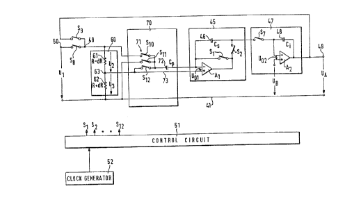
Fig. 4 shows an example of embodiment of the signal processing
circuit 2 of Fig. 1 for the signal processing of the sensor
signal furnished by a resistance half-bridge 60 and Fig. 5
shows the time profile of the associated switch control signals
and voltages. The resistance half-bridge 60 contains two
2~~~2~~
resistors 61,62 which are connected in series between a
terminal 40 and a reference conductor 41 and the connection
point of which forms a tap 63.
The resistance values of the resistors 61 and 62 differ from
an identical basic value R by the same amounts dR, which are
however of opposite sign. As example, it is indicated that the
resistor 61 has the value R-dR and the resistor 62 the value
R+dR. The resistor half-bridge 60 may therefore be formed for
example by the force sensor 20 of Figs. 2 and 3, the resistors
61 and 62 representing the resistance values of the strain
gauges 23 and 22 respectively. R is the resistance value of
the undeformed strain gauge and dR is the resistance change
effected by the deformation of the strain gauge. The resistance
ratio dR/R represents the measuring effect M of interest which
in the case of the force sensor 20 of Figs. 2 and 3 gives the
relationship between the force F to be measured and the
resistance change of the strain gauges.
For better understanding the functional processes the sensor 60
in Fig. 4 is inserted between two circuit blocks of the signal
processing circuit but in reality it will be spatially separate
from the signal processing circuit, which may be configured as
integrated circuit, and connected to the latter via shielded
lines. The signal processing circuit operates by the principle
of charge balancing with switch-capacitor combinations. Whereas
however such signal processing circuits usually convert the
analog sensor signal to a digital output signal representing
the measured value, the signal processing circuit of Fig. 4 is
constructed in a particular manner so that it furnishes an
analog output signal.
The sensor 60 is connected on the one hand to a function
block 70 and on the other hand to a buffer 45. The function
block 70 contains a switch group 71, a capacitor 72 with
capacitance Cp and a continous connecting conductor 73 which
connects the tap 63 of the resistance half-bridge 60
...~ 20~0~00
6
permanently to the noninverting input of an operational
amplifier A1 in the buffer 45. The switch group 71 contains
three switches S10, S11 and S12. The one electrode of the
capacitor 72 is permanently connected to the inverting input
of the operational amplifier A1. The other electrode of the
capacitor 72 is connected by the switch S10 to the input
terminal 40, by the switch S11 to the reference conductor 41
and by the switch S12 to the connecting conductor 73.
The resistor half-bridge 60 forms a voltage divider at which
when the switch S8 is closed a supply voltage U1 is present
and when the switch S9 is closed the output voltage UA. The
voltage present between the terminal 40 and the tap 63 at the
resistor 61 is denoted by U2 and the voltage present between
the tap 63 and the reference conductor 41 at the resistor 62
is denoted by U3.
The buffer 45 contains the operational amplifier Ai, a storage
capacitor 46 of a capacitance Cs and two switches S1, S2. When
the switch S1 is closed it connects the output of the amplifier
A1 to the inverting input thereof. When the switch S2 is closed
it connects the output of the operational amplifier A1 to the
one electrode of the storage capacitor 46, the other electrode
o~f which is connected to the inverting input of the operational
amplifier A1 so that the storage capacitor 46 then lies in the
feedback circuit of the operational amplifier A1. The non-
inverting input of the amplifier Al lies at the tap 63. The
potential at the inverting input differs from that of the non-
inverting input by the offset voltage U~1 of the operational
amplifier A1.
The buffer 45 is followed by an integrator 47. The integrator
47 includes an operational amplifier A2, an integration
capacitor 48 of capacitance C1 lying in the feedback circuit
of the operational amplifier A2 and a switch S7. When the
switch S7 is closed it connects the inverting input of the
operational amplifier A~ to the storage capacitor 46 in the
_ 2Q~~26~
7
buffer 45 is followed by an integrator 47. It includes an
operational amplifier A2, an integration capacitor 48 of
capacitance Ci lying in the feedback circuit of the operational
amplifier A2 and a switch S7. When it is closed it connects the
inverting input of the operational amplifier A2 to the storage
capacitor 46 in the buffer 45. The noninverting input of the
operational amplifier A2 is connected to a fixed potential
which differs by a voltage UB from the potential of the
reference conductor 41. The potential at its inverting input
differs from the fixed
potential of the noninverting input by the offset voltage U02
of the operational amplifier A2. The output of the operational
amplifier A2 is connected to the output terminal 49 of the
signal processing circuit. Between the output terminal 49 and
the reference conductor 41 the output voltage UA appears.
When it is closed, a switch S8 connects the terminal 40 to an
input terminal 50 and a switch S9, when it is closed, connects
the terminal 40 to the output terminal 49. In operation of the
circuit between the output terminal 50 and the reference
conductor 41 a supply voltage U1 is applied which corresponds
to the supply signal V of Fig. 1.
The switches S1, S~,, and S7 to S12 are actuated by control
signals which are furnished by a control circuit 51 which is
synchronized by a clock signal fed by a clock generator 52. For
simplification the clock signals are denoted by the same
reference numerals S., as the switches controlled by them.
Each switch S., is open when the signal controlling it has a
low signal value and is closed when the signal controlling it
has a high signal value. The switches S., are represented
symbolically as mechanical switch contacts but in reality of
course they are hic~hspeed electronic switches, for example
field-effect transistors.
8
The mode of opreation of the signal processing circuit of
Fig. 4 will now be explained with the aid of Fig. 5.
Apart of the already mentioned time profile of the control
signals S1 to S12 the diagrams of Fig. 5 also show the time
profile of the voltage UCs at the storage capacitor 46 and the
output voltage UA in the course of several consecutive
cycles Z. Each cycle Z is divided into six phases denoted
1 to 6.
The switches S1 and S2 are controlled by a periodic square-
wave signal in antiphase manner so that the switch S1 is open
when the switch S2 is closed and vice-versa. The switches S1
and S2 assume their alternating states in each case for the
duration of one of the phases 1 to 6. When the switch S1 is
closed and the switch S2 is open, which is the case in each of
the phases 1, 3 and 5 of each cycle Z, the capacitor lying in
the input circuit of the operational amplifier A1 can be
applied by one of the switches S10 to S12 to one of the
voltages U2, U3 or U01 and correspondingly charged without
thereby influencing the charge in the storage capacitor 46.
The circuit is then in a conditioning phase for the
conditioning of the capacitor 72. If on the other hand the
switch S1 is open and the switch S2 is closed the buffer 45 is
ready for the transfer of charge from the capacitor 72 to the
storage capacitor 46.
The switches S8 and S9 are likewise controlled by a
periodic square-wave signal in antiphase manner so that the
switch S8 is open when the switch S9 is closed and vice-versa.
During the phases 1 to 4 of each cycle Z the switch S8 is
closed and the switch S9 is open. The phases 1 to 4 of each
cycle Z thus form a subcycle Z1 in which the voltage U1 is
applied to the resistor half-bridge 60. In contrast, in phases
and 6 the switch S9 is closed and the switch S$ open. The
phases 5 and 6 thus form a subcycle ZA in which the voltage UA
is applied to the resistor half-bridge 60.
9
In each subcycle 2:1 in which the voltage U1 is applied to the
resistor half-bridge 60 the voltages U2 and U3 have the
following values:
R-dR R-dR
U2(1-4) ~I1 . (R-dR) + (R+dR) U1 . 2R ( 1 )
R+dR R+dR
U3(1-4) - U1 ' (R-dR) + (R+dR) U1 . 2R (2 )
In each subcycle ~'.A in which the voltage UA is applied to the
resistor half-bridge 60 the voltages U2 and U3 have the values
R-dR R-dR
U2 (5 ~ 6) - lIA ' (R-dR) + (R+dR) UA ~ 2R ( 3 )
R+dR R+dR
U3(5~6) - lIA ' (R-dR) + (R+dR) UA ~ 2R ( 4)
The signal processing circuit of Fig. 4 operates
by the principle of charge balancing which takes place
in the storage capacitor 46. The function block 70 furnishes
discrete charge packets which are transferred to the storage
capacitor 46. Said' charge packets are generated in that the
capacitor 72 is alternately charged and reverse charged by
the different voltages U2, U3 and U01 with the aid of the
switches 510. S11' 512' The charge packets stored in the
storage capacitor 46 and summated are transferred by closing
the switch S7 to the integration capacitor 48. With the time
profile of the various switch control signals illustrated in
Fig. 8 the following time sequence results for the operation
of the signal processing circuit of Fig. 4:
2~~~~~~
l0
D4,~r.~, 1 .
At the start of phase 1 of each cycle Z the charge applied in
the preceding cycle is still present on the storage capacitor
46. For the duration of the phase 1 the switch S1 is closed
and the switch S2 open so that the storage capacitor 46 is
separated from the output of the operational amplifier A1. The
switch S7 is closed for the duration of the phase 1 so that a
charge transfer takes place from the storage capacitor 46 to
the integration capacitor 48. The storage capacitor 46 is
thereby discharged to the residual charge
TICS (R) - (U02 - U01) ~ Cs ( 5 )
the reverse charoe amount fl.owino to the intParation canaci.tor 4.8.
Furthermore, for the duratian of the phase 1 the circuit is in
the conditioning phase for the capacitor 72 because the switch
S1 is closed and the switch S2 is open. Since at the same time
the swich S11 is closed, the capacitor 72 is connected to the
reference conductor 41 so that it is charged to the charge
_ QCp(1) - (U01 U3(1-4)) ~ Cp ( b )
without the charge of the storage capacitor 46 being
influenced by this charging operation.
D4,~~.0 9.
In phase 2 of each cycle Z the switch S1 is open and the
switch S2 closed so that the buffer 45 is ready for the
transfer of charge to the storage capacitor 46. At the same
time the switch S1,2 is closed so that the capacitor 72 is
connected via the .connecting conductor 73 to the noninverting
input of the operational amplifier A1. As a result, at the
capacitor 72 only -the offset voltage U01 is present by which
it is reverse char~3ed to the charge
qCP(2) U01 Cp (7 )
It
11
The reverse charge amount
dQ~P(1~2~~ Q~P(2) Q~P(1) 03(1-4) ~P (8)
flows to the storage capacitor 46 and causes a negative change
of the voltage U~;s as is apparent from the associated diagram
of Fig . 5.
,.. Ph~cn Q
In phase 3 the switch S1 is again closed and the switch S2
open so that the circuit is in the conditioning phase for the
capacitor 72. However, the switch S7 remains open so that no
charge transfer takes place from the storage capacitor 46 to
the integration capacitor 48 and the storage capacitor retains
its charge. Furthermore, the switch S10 is now closed so that
the capacitor 72 is connected to the terminal 40 and is thus
charged to the charge
OOP(3) (001 02(1-4)) ~ Op (9 )
D 4. .~. r. .~. A .
In phase 4 the switch S1 is open and the switch S2 closed so
that the buffer 45 is ready for the transfer of charge. At the
same time the switch S12 is again closed so that the capacitor
72 is connected via the connecting conductor 73 to the
noninverting input of the operational amplifier A1 and by the
offset voltage U01 is reverse charged to the charge
Q~P (4) 001 ~ ~p ( 10~
The reverse charge amount
dQOP(3,4;1 qCp(4) QCp(3) 02(1-4) ~ OP (11)
12
flows to the storage capacitor 46 and causes a positive change
of the voltage U~;s as is apparent from the associated diagram
of Fig. 5. This F~ositive voltage change is however smaller
than the negatives voltage change caused in the phase 2 because
the voltage U2(1_4) is less than the voltage U3(1-4)'
Thus, in the phases 1 to 4 altogether a measuring charge
packet
... dQM = dQCP ( 1,'2) + dQCP (3 ~ 4) U2 ( 1-4) ~ CP U3 ( 1-4) ~ Cp (12 )
has been transferred to the storage capacitor 46. If the values
from the equations (1 ) and (2 ) are inserted for U2(1-4) and
U3(1-4)' this gives
dQM = U1 ~ Cp (R-dR) /2R - U1 ~ Cp (R+dR) /2R = -U1 ~ Cp ~ dR/R (13 )
The difference bevtween the changes of the voltage UCs caused
in phases 2 and 4 is proportional to this measuring charge
packet dQM, as is indicated in the associated diagram of Fig. S.
Phase 5:
Phase 5 is again ~~ conditioning phase for the capacitor 72.
Since the switch ;>10 is closed, the capacitor is charged to
the charge
QCp(5) - (U01 02(5,6)) ~ CP (14)
Phase 6:
In phase 6 the switch S11 is closed so that the capacitor 72
is connected to the reference conductor 41 and is reverse
charged to the charge
13
QCP(6) (U01 U3(5,6)) CP (15)
The reverse charge amount is transferred as compensation
charge packet
dQK = QCp(6) - QCP(5) U2(5,6) - CP+ U3(5,6) - CP (16)
to the storage capacitor 46. If the values from the equations
and ( 4 ) are inserted for U2(5,6) and U3(5,6) ~ this
gives,
dQK = UA ~ C;p (R-dR) /2R + UA - Cp (R+dR) /2R = UA ~ Cp (17 )
The compensation charge packet dQK causes a positive change of
the voltage UCs proportional thereto as is indicated in the
corresponding diagram of Fig. S.
Each cycle Z may consist of n subcycles Z1 and k subcycles ZA;
Fig. 5 shows the relationships for the special case n = k = 1.
In the general case in each cycle Z the charge
QCs (Z) - QCs (R) + n ~ dQM + k - dQK ( 18~
has collected on the storage capacitor 46. At the start of the
following cycle Z the storage capacitor 46 is again discharged
to the residual charge QCs(R)- The differential charge
dQ = n ~ dQM + k ~ dQK ( 19)
is transferred to the integration capacitor 48, thereby
regulating the output voltage UA. The circuit thus operates as
a closed loop whi~~h tends to bring the output voltage UA to a
a
14
value at which the sum of the k compensation charge packets
dQK is equal to the sum of the n measuring charge packets dQM.
When this charge is reached, charge balance exists in the
storage capacitor 46:
n ~ dQM + k - dQK = 0 (20 )
By inserting the values for dQM and dQK from the equations
(13) and (1~1, this gives the transfer function of the
circuit:
UA n dR
- - - ' - (21)
U1 k R
The ratio of the analog output voltage UA to the supply voltage
U1 therefore indicates in the steady state the desired
resistance ratio directly. In Fig. 5 it is assumed that the
steady state has arisen at the instant tE at the end of the
second cycle Z i7Llustrated. From this instant on the voltage
UA no longer changes as long as the resistances 61 and 62
retain their values. On a change of the resistance ratio dR/R
the output voltage UA changes to another value with a time
constant defined by the capacitance C1 of the integrated
capacitor 48.
The capacitance value of the capacitor 72 does not enter the
transfer function but it does govern the magnitude of the
charge packets and thus the dimensioning of the capacitors 46
and 48. Likewise, the capacitance values of the capacitors 46
and 48, the offset voltages of the operational amplifiers, the
supply voltage of the circuit and the frequency with which the
control circuit is clocked do not enter the final result.
The value of the voltage U1 is limited only by the working
range of the circuit. If the current supply voltage of the
circuit is chosen as supply voltage U1, then in accordance
15
with equation (21) an output signal is obtained which is
proportional to the: current supply voltage.
If a fixed reference voltage Uref is chosen as supply
voltage U1 then in accordance with equation (21) an absolute
output signal is obtained.
Fig. 6 shows a modification of the circuit of Fig. 4 which
furnishes an analog' output current IA instead of an analog out-
put voltage UA. In Fig. 6 the buffer 45 and the integrator 47
of Fig. 4 are each represented by a circuit block 80 consisting
of the resistor half-bridge 60 and the function block 70 of
Fig. 4.
In Fig. 6 the output of the integrator 47 is connected to the
base of an n-p-n transistor 81 which is connected as emitter
follower with a re:;istor 82 of value RA lying in the emitter
circuit. The feedback leading to the switch S9 is connected to
the emitter of the transistor 81. The output voltage UA of the
integrator 47 causes the output current IA to flow through the
collector-emitter circuit of the transistor 81. Thus, with
this circuit the ve~ltage
BRA = Rp ' Ip ( 22)
is fed back to the input. Thus, for the compensation charge
packet dQK instead of the equation (17):
dQK = U~ Cp (23)
Accordingly, instead of equation (20) the transfer function is:
IA/U1 =[n/(kRA)](dR/R) (24)
16
The circuit of Fig. 6 is particularly suitable for measuring
arrangements in which the measured value signal is transmitted
in the form of a direct current via a single two-conductor
line, said current being variable for example between 4 mA and
20 mA and also comprises the supply current for the sensor and
the signal processing circuit.