Note: Descriptions are shown in the official language in which they were submitted.
PHA 21.607 1 20.02.1991
Circuit arrangernent.
This is an invention in the lighting art. More particularly, it involves an
arrangement for predicting the end of lamp life in fluorescent lamps in a series two
lamp system.
One of the objects of the invention is to provide improved fluorescent
S lamp lighting systems.
In two lamp fluorescent systems employing electronic ballasts the lamp
electrodes are pre-heated before ignition takes place. rf, for some reason, the lamps fail
to ignite, the heating cycle can be repeated and the ignition stage can once again be
attempted in order to cause the lamps to ignite. In a two lamp system where one of the
10 lamps has deteriorated and will not ignite this recycling procedure can cause the other
lamp to flash continuously to the annoyance of anyone near the fixture in which the
lamps are mounted.
One of the advantages of this invention is that it prevents the flashing of
fluorescent lamps for more than a predetermined period of time.
It is a feature of the invention to restart the recycling process in an
attempt to ignite lamps in a two-lamp system where a deteriorating larnp has been
removed from the system and replaced with a new lamp.
In accordance with one aspect of the invention, there is provided a
Iighting arrangement suitable for two fluorescent lamps including a ballast means for
20 providing power to said two lamps to illuminate them. The ballast means provides
power for pre-ignition heating, for ignition and for post-ignition operation of the lamps.
The ballast is operabie to attempt to ignite said lamps repeatedly should they fail to
ignite. The arrangement also includes shut-off means for causing the ballast means to
cease trying to ignite the lamps after a predetermined time during which at least one of
25 the lamps has failed to ignite.
In accordance with another aspect of the invention there is provided a
circuit arrangement suitable for two fluorescent lamps including a ballast means for
2~63~
PHA 21.607 2 20.02.1991
providing power to the two lamps to ignite them. The ballast means is operable to
attempt to ignite the lamps repeatedly should they fail to ignite. The ballast means
provides substantially equal voltage to the lamps when they are operating in a
prescribed manner. The arrangement also includes sensing means which sense that the
voltage across each of the two lamps is not substantially equal. In response thereto, the
sensing means operates to an operated condition wherein it prevents the ballast means
from continuing to attempt to ignite the lamps.
Other objects, features and advantages of the invention will be apparent
from the following description and appended claims when considered in conjunction
with the accompanying drawing in which:
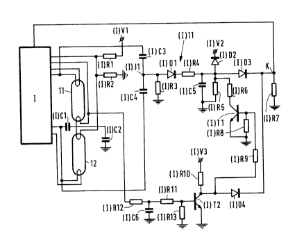
figure 1 shows a ballast means connected to two fluorescent lamps with
the addition of one version of the lamp life prediction circuit of this invention, and
figure 2 shows a ballast means connected to two fluorescent lamps with
an alternate version of the lamp life prediction circuit of this invention.
In figure 1, I is a ballast means for providing power to fluorescent lamps
11 and 12 for preignition heating, for ignition and for post-ignition operation of said
lamps. Ballast means I is operable to attempt to ignite said lamps repeatedly should
they fail to ignite. Such a ballast means is for instance described in European Patent
Application 0351012.
The improvement discloses herein involves the provision of the
prediction circuitry I(11). As shown in figure 1 prediction circuit (1)11 includes a
resistor (I)R1 connected to a voltage source (I)V1 and to one electrode of lamp 12.
That electrode of lamp 12 is also connected to ground through a resistor (I)R2. That
same electrode of lamp 12 is connected directly to one of the electrodes of lamp 11 and
to the other electrode of lamp 12 through capacitance (I)C1. The interconnected
electrodes of lamps 11 and 12 are also connected to ground through capacitor (I~C2.
The upper electrode of lamp 11 is connected through a capacitor (I)C3 to a junction
point (I)JI. Junction point (I)J1 is connected through a capacitor (I)C4 to the lower
electrode of lamp 12. Lamps 11 and 12 and capacitors (I)C3 and (I)C4 form a bridge
through which capacitor ~I)C5 may be charged under prescribed conditions to be
described.
~04~367
PHA 21.607 3 20.02. 1991
Junction point (I)J1 is connected to ground through resistor (I)R3 and to
capacitor (I)C5 through diode (I)D1 and resistor (I)R4. Capacitor (I)C5 is also
connected to a second voltage source (I)V2 through diode (I)D2, which keeps capacitor
(I)C5 from charging to a voltage higher than (I)V2. Capacitor (I)C5 is also connected
5 to terminal K. Resistor (I)R5 is connected in parallel with capacitor (I)C5. The junction
of diodes (I)D2 and (I)D3 is connected to the collector of transistor (I)T1 through
resistor (I)R6. Terminal K is connected to ground through resistance (I)R7 and
connected to a ballast means I. The emitter of transistor (I)TI is connected to ground.
Its base is connected through resistor (I)~R8 to ground and also through resistor (I)R9 to
10 the collector of transistor (I)T2. The collector of transistor (I)T2 is also connected to a
voltage source (I)V3 through resistor (I)RI0 and to terminal K through diode (I)D4.
The emitter of transistor (I)T2 is grounded while its base is connected through resistors
(I)Rl 1 and (I)R12 to the circuit including the middle electrodes of lamps 11 and 12.
The base of transistor (I)T2 is connected to ground through resistor (I)R13. The15 junction between resistors (I)R11 and (I)R12 is also connected to ground through
capacitor (I)C6.
As mentioned, capacitors (I)C3 and (I)C4 form a bridge circuit with
lamps 11 and 12. The sizes of the capacitance of capacitors (I)C3 and (I)C~ are chosen
to ke p the bridge output voltage low during normal lamp operation. Thus, if lamps 11
20 and 12 have substantially the same operating characteristics, capacitors (I)C3 and (I)C4
should be equal so the bridge will be balanced and no significant voltage relative to
ground will appear at junction point (I)J1 because the voltage across each lamp will be
substantially equal to that across the other. If the performance of one of the lamps
deteriorates so that it will not ignite, the bridge output voltage will remain high due
25 mainly to the effect of capacitor (I)C1 which is connected across lamp 12. As a result,
the voltage stored on capacitor (I)C5 will increase. After a prede~ermined time set by
the values of resistor (I)R4 and capacitor (I)C5, the voltage on terminal K will reach a
prescribed value.
When this prescribed value is reached, the signal at terminal K stops the
30 attempts of ballast means I to ignite the lamps. This can for instance be realized by
rendering a switching element between the supply voltage source and the ballast means
non-conducting as soon as the signal at terminal K reaches the prescribed value.
20~3~7
PHA 21.607 4 20.02.1991
Another possibility, in case the configuration of ballast means I is as described in
European Patent Application 0351012, is to connect terminal K to line "V LAMP". If
the voltage on line "V LAMP" reaches the prescribed value, above that of the voltage
on line "V REG", the frequency control of the ballast means will cause line "START"
5 to be grounded. As long as line "START" remains grounded, the system remains in its
pre-ignit;on operation condition and will be prevented from trying to ignite lamps 11
and 12.
In order to allow ignition to be repeated when a bad lamp is replaced by
a good one, transistor (I)T2 is employed to sense the removal of the bad lamp. It does
10 this when the trickle current provided by source (I)V1 through the center electrodes of
lamps 11 and 12 ceases while the lamp is removed. This lack of trickle current causes
transistor (I~T2 to turn-off which holds the voltage on terminal K high as well as
turning transistor (I)T1 on to discharge capacitor (I)C5. Upon replacement of the bad
lamp with a good one, transistor (I)T2 is once again turned on by the trickle current
through the center electrodes of lamps 11 and 12. As a consequence of transistor (I)T2
being turned on, transistor (I)T1 is turned-off. As a result of capacitor (I)CS being
discharged the voltage at terminal K is no longer above the prescribed value thereby
permitting the ballast means I to try to ignite lamps 11 and 12.
Figure 2 shows a prediction circuit which functions in substantially the
20 same manner as the prediction circuit in figure 1. The difference between thearrangement in figure 2 and that in figure 1 is that the current through the center
electrodes of lamps 11 and 12 is sensed through a resistor (I)R14 and a small
transformer (I)TRI. In addition, resistor (I)R12 shown in figure 1 is replaced by diode
(I)D12 in figure 2. A comparison of figure 1 with figure 2 will show that like elements
25 have been identified by the same reference characters in both figures.
It should be apparent that various modifications of the above will be
evident to those skilled in the art and that the arrangement described herein is for
illustrative purposes and is not to be considered restrictive.