Note: Descriptions are shown in the official language in which they were submitted.
'' o
2046530
OPTOELECTRONIC WIDE BANDWIDTH PHOTONIC
BEAMSTEERING PHASED ARRAY
BACKGROUND OF THE INVENTION
The disclosed invention is generally directed to beam-
steered phased arrays for radar, and is directed more
particularly to a photonically beamsteered phase array that
utilizes a photonic true time delay circuit for both
transmit and receive functions.
A beamsteered phased array is an antenna system
comprising individual antenna elements whose antenna beam
direction (i.e., pointing direction) is controlled by the
relative phases of the signals respectively radiated or
received by the antenna elements. In particular, for
transmission, the relative phases of the energy radiated by
the individual antenna elements is controlled to define the
transmit beam direction of the antenna. For recei~ing, the
relative phases of the energy received by the individual
elements is controlled to define the receive beam direction
of the antenna. The premise of a true time delay beam-
steered phased array is to steer the array beam by intro-
ducing known time delays into the respective signalstransmitted or received by the respective antenna elements.
Photonic true time delay circuits having optical fiber
delay lines have attributes that would make them well
suited for phased arrays. Such attributes include rela-
tively wide bandwidth, low loss in the fiber, capability
2~4~3~
for long delays, small size, low weight, resistance to
electromagnetic interference, low cross-talk, and the
capability of being remotely located from other components
in a phased array.
However, optical fiber delay lines are unidirectional,
and thus cannot be used in a manner similar to known bi-
directional phase shifters. A relatively direct approach
to dealing with such uni-directionality would be to utilize
separate optical fiber time delay circuits in the transmit
and receive paths of the phased array. However, due to
considerations including complexity, noise, and dynamic
range, photonic elements might not be acceptable in the
receive path which must communicate signals of extremely
low power.
SUMMARY OF THE INVENTION
It would therefore be an advantage to provide a phased
array that utilizes photonic true time delay beamsteering
without having photonic beamsteering in the direct receive
path.
Another advantage would be to provide a phased array
that utilizes photonic interconnects for the respective
transmit/receive circuits of the array.
The foregoing and other advantages are provided by the
invention in a phased array transmit/receive circuit for
each of the antenna elements of the phased array. The
transmit/receive circuit includes an optical fiber true
time delay circuit responsive to an electrical RF signal
for providing an optical signal having a controlled time
delay, an optical fiber for propagating the time delay
controlled optical signal, an optical detector circuit
responsive to the propagated time delay controlled optical
signal for providing a time delay controlled electrical
signal, transmit circuitry responsive to the time delay
3 2046~3~
controlled electrical signal for providing to the associat-
ed antenna element a transmit signal based on the time
delay controlled electrical signal, and receive circuitry
responsive to the time delay controlled electrical signal
and the signal received by the associated antenna element.
A first RF switch selectively couples the time delay
controlled electrical signal to the transmit circuit during
transmit times, and to the receive circuit during receive
times; and a second RF switch couples the associated
antenna element to the transmit circuit during transmit
times, and to the receive circuit during receive times.
The invention more particularly includes true time
delay processing means for time aligning the received
signal with respect to the received signals of the other
transmit/receive circuits of the phase array.
Other aspects of this invention are as follows:
In a phased array radar system having a radar
processor and a plurality of antenna elements, a trans-
mit/receive circuit for each of the antenna elements
comprising:
an optical fiber true time delay circuit respon-
sive to an electrical RF signal for providing an
optical signal having a controlled time delay relative
to the outputs of the optical fiber true time delay
circuits of the other transmit/receive circuits in the
array;
optical means for propagating said true time
delay controlled optical signal;
optical detection means responsive to the propa-
gated true time delay controlled optical signal for
providing a true time delay controlled electrical
signal;
transmit means responsive to said true time delay
controlled electrical signal for providing a transmit
signal based on said true time delay controlled
electrical signal to the associated antenna element;
,~
- 3a 2~4653~
receive means responsive to said true time delay
controlled electrical signal and the signal received
by the associated antenna element for providing a
baseband received signal, said true time delay con-
trolled electrical signal being utilized as the local
oscillator freguency to provide the correct phase for
steering the array;
true time delay processing means responsive to
said baseband received signal for providing a digital
received signal that is properly aligned relative to
the digital received signals provided by the receive
means of the other transmit/receive circuits of the
array;
first switching means for coupling said true time
delay controlled electrical signal to said transmit
means during transmit times, and to said receive
means during receive times; and
second switching means for coupling the associat-
ed antenna element to said transmit means during
transmit times, and to said receive means during
receive times.
In a phased array radar system having a radar
processor and a plurality of antenna elements, a trans-
mit/receive circuit for each of the antenna elements
comprising:
an optical fiber true time delay circuit respon-
sive to an electrical RF signal for providing an
optical signal having a controlled time delay relative
to the outputs of the optical fiber true time delay
circuits of the other transmit/receive circuits in the
array;
optical means for propagating said true time
delay controlled optical signal;
optical detection means responsive to the propa-
gated true time delay controlled optical signal for
providing a true time delay controlled electrical
signal;
`'' h
~ 3b
~6~3~
transmit means responsive to said true time delay
controlled electrical signal for providing a transmit
signal based on said true time delay controlled
electrical signal to the associated antenna element;
receive means responsive to said true time delay
controlled electrical signal and the signal received
by the associated antenna element for providing a
h~^h~n~ received signal, said true time delay con-
trolled electrical signal being utilized as the local
oscillator frequency to provide the correct phase for
steering the array;
analog to digital conversion means responsive to
said baseband received signal for providing a digital
received signal;
optical means responsive to digital received
signal for providing an optical received signal to the
radar processor;
first switching means for coupling said true time
delay controlled electrical signal to said transmit
means during transmit times, and to said receive
means during receive times; and
second switching means for coupling the associat-
ed antenna element to said transmit means during
transmit times, and to said receive means during
receive times.
In a phased array radar system having a radar
processor and a plurality of antenna elements, a trans-
mit/receive circuit for each of the antenna elements
comprising:
an optical fiber phase true time delay circuit
responsive to an electrical RF signal for providing an
optical signal having a controlled time delay relative
to the outputs of the optical fiber true time delay
circuits of the other transmit/receive circuits in the
array;
optical means for propagating said true time
delay controlled optical signal;
'~-
`~ 3c 2046530
optical detection means responsive to the propa-
gated true time delay controlled optical signal for
providing a true time delay controlled electrical
signal;
transmit means responsive to said true time delay
controlled electrical signal for providing a transmit
signal based on said true time delay controlled
electrical signal to the associated antenna element;
receive means responsive to said true time delay
controlled electrical signal and the signal received
by the associated antenna element for providing a
baseband received signal, said true time delay con-
trolled electrical signal being utilized as the local
oscillator frequency to provide the correct phase for
steering the array;
first switching means for coupling said true time
delay controlled electrical signal to said transmit
means during transmit times, and to said receive
means during receive times; and
second switching means for coupling the associat-
ed antenna element to said transmit means during
transmit times, and to said receive means during
receive times.
BRIEF DESCRIPTION OF THE DRAWINGS
The advantages and features of the disclosed invention
will readily be appreciated by persons skilled in the art
from the following detailed description when read in
conjunction with the drawing wherein:
FIG. 1 is a block diagram of a photonically beam-
steered phased array in accordance with the invention.
FIG. 2 is a block diagram of one of the array trans-
mit/receive modules of the photonically beam steered phased
array of FIG. 1.
FIG. 3 is a schematic block diagram illustrating the
geometrical considerations in a true time delay beamsteered
phased array.
..
~e ~
4 2046~3~
DETAILED DESCRIPTION OF THE DISCLOSURE
In the following detailed description and in the
several figures of the drawing, like elements are identi-
fied with like reference numerals.
Referring now to FIG. 1, set forth therein is a broad
bandwidth phased array radar system 10 in accordance with
the invention. The radar system includes a radar processor
11 and a radar display 13 responsive to the radar processor
11. The radar processor further controls an RF exciter
source 15 whose output provided to an RF amplifier 17. The
output of the RF amplifier 17 is split by an RF splitter
circuit 19 which provides RF inputs to a plurality of fiber
optic true time delay circuits 21. By way of illustrative
example, each true time delay circuit 21 provides true time
delay via fiber optic line length switching as disclosed in
"Wideband Fibre-Optic Delay Network For Phased Array
Antenna Steering," Ng, Walston, Tangonan, Newberg, Lee,
~T~CTRONICS LETTERS, Vol 25, No. 21, October 12, 1989,
pages 1456-1457, and "Electro-Optical Switch for Antenna
Beamsteering," Newberg, Walston, Lee, Ng, Tangonan, SPIE
PROCEEDINGS - Optoelectronic Signal Processinq for Phased-
Arrav Antennas II, Vol. 1217, January 1990, pages 126-131.
The optical outputs of the fiber optic true time delay
circuits 21 are communicated via respective fiber optic
cables 23 to respective transmit/receive array modules 25.
The modules 25 are coupled to respective antenna elements
27.
By way of illustrative example, respective fiber optic
cables 29 are utilized for communicating multiplexed
control signals from the radar processor 11 to the array
modules 25, and respective fiber optic cables 31 are
utilized to communicate received digital signals from the
array modules to the radar processor 11.
-
5 2~46~3~
By utilizing fiber optic cables for transferring
control signals, data, and the true time delayed signals,
the array modules 25 can be remotely located from the rest
of the phased array radar system. The only electrical
5connections would be for DC voltage input and RF power
output to the antenna elements 27.
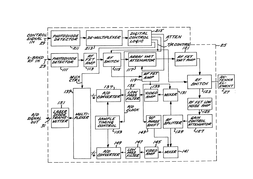
Referring now to FIG. 2, shown therein is a block
diagram of one of the array transmit/receive modules 25
which includes a photodiode detector circuit 111 that
10produces an electrical RF signal in response to the RF
optical signal communicated via the fiber optic cable 23.
The RF output signal of the photodiode detector circuit 111
is provided to an RF amplifier 113 which provides its
amplified RF signal to an RF switch 115 that is controlled
15by a transmit/receive control signal T/R CONTROL. The RF
switch 115 is controlled to couple the amplified RF signal
to an array transmit attenuator circuit 117 during transmit
times and to an RF amplifier 119 during receive times.
The output of the transmit attenuator 117 is coupled
20to a transmit RF amplifier 121 whose output is provided to
an RF switch 123. The RF switch 123 is further coupled to
the antenna element 27 associated with the particular array
module and also to a receive RF amplifier. The RF switch
123 is controlled by the transmit/receive control signal
25T/R CONTROL to couple the output of the transmit RF ampli-
fier 121 to the antenna element 27 during transmit times,
and to couple the antenna element 27 to the receive RF
amplifier 125 during receive times.
In the receive path, the output of the receive RF
30amplifier 125 is provided to a gain control attenuator 127
whose output is split into two components by an RF power
splitter 129.
One output of the power splitter 129 is provided to a
mixer 131 which receives the output of the RF amplifier 119
35as the local oscillator signal. The output of this in-
~ 6 20~6S30
phase mixer 131 is an in-phase baseband component of the
received signal, and is coupled to a video amplifier which
provides its output to a low pass filter 135. The output
of the low pass filter 135 provides the analog input to an
analog-to-digital (A/D) converter 137. The digital output
of the A/D converter 137 is provided to a multiplexer 139.
The other output of the power splitter 129 is provided
to a mixer 141 which receives, via a 90 degree phase shift
circuit 143, a 90 degree phase shifted version of the
output of the RF amplifier 119 as the local oscillator
signal. The output of this quadrature mixer 141 is a
quadrature baseband component of the received signal, and
is coupled to a video amplifier 145 which provides its
output to a low pass filter 147. The output of the low
pass filter 147 provides the analog input to another
analog-to-digital (A/D) converter 149. The digital output
of the A/D converter 149 is provided to the multiplexer 139
which provides a time-multiplexed signal of the A/D outputs
to a laser diode transmitter. The laser diode transmitter
provides its optical output to the fiber optic cable 31
(FIG. 1) associated with the particular array module.
The sample timing of the A/D converter 137, 149 is
controlled by a sample timing control circuit 153 to
provide the appropriate true time delay of the A/D sampling
so as to properly align the pulse energy of the signals
received by the different transmit/receive modules in the
phased array. As discussed further herein, geometrical
considerations as to the locations of the array antenna
elements results in a return pulse being received by the
antenna elements at different times when the pointing
direction is other than broadside.
The array module 25 further includes a photodiode
detector circuit 211 for detecting the optical signal
communicated via the associated control signal fiber optic
cable 29. The electrical output of the photodiode detector
7 2~4~3~
circuit 211 is provided to a de-multiplexer 213 which
provides its output to a digital control logic circuit 215.
The control logic circuit 215 provides the transmit/receive
signal T/R CONTROL to the RF switches 115, 123; the trans-
mit attenuate control signal ATTEN to the transmit attenu-
ator circuit 117; the sample timing master clock A/D CLOCK
to the sample timing control circuit 153; and the receive
data multiplexer control signal MUX CTRL.
Referring now to FIG. 3, the true time delay needed
for beamsteering can be looked at in two parts: the time
delay or phase needed to steer the continuous wave (CW)
carrier, and the time delay needed to align the pulse
modulation on the carrier (i.e., the pulse energy). The
antenna phase and energy wavefront can be represented by a
line normal to the array pointing direction and is wherein
the transmitted or received RF energy is in phase and
aligned in pulse energy.
To point the antenna array correctly for transmitting,
as to all of the antenna elements, the phase of the energy
must be the same along the-RF wavefront line and the pulse
energy must be there at the same time.
To receive the RF signal from the desired pointing
direction, the RF wavefront as received by the antenna
elements must be appropriately delayed for each element
such that "effectively" the phase of the energy would be
all the same at each of the radiating elements and the
pulse energy "effectively" arrives at each of the antenna
elements at the same time. In the subject invention, such
phase and time alignment is "effectively" achieved by phase
and delay adjustments made after the RF energy is received,
such that the signals received by the respective antenna
elements are in phase and pulse energy aligned in time
prior to summing to form the received beam. In other
words, the RF wavefront is adjusted after it reaches the
antenna elements.
-
2~53~
For transmit, time delay beamsteering delays thecarrier and the modulation energy by a time which causes
both the phase of the carrier and the energy in the carrier
and its modulation to correctly arrive along the RF wave-
front line on transmit, and "effectively" arrive at eachradiating element on receive at the same phase at and at
the same time, independent of frequency. For the received
signal, the value of the phase needed to steer the carrier
can be generated by true time delay in the LO path as
discussed below. As also discussed below, the value of the
time delay needed to acing the energy can be obtained by
appropriately delaying the clocks at the A/D converters in
the receive paths for the respective antenna elements.
Simply stated, time delay on transmit and on receive
as discussed above is utilized to achieve substantially the
same result if elements were repositioned to be normal to
the pointing direction, as would be provided with a mechan-
ical scan antenna.
As a result of true time delay beamsteering via fiber
optic line length switching, wide bandwidth and wide
instantaneous bandwidth are achieved. Wide bandwidth means
the signal carrier frequency can be changed over a wide
range, while wide instantaneous bandwidth means the signal
carrier modulation is such as to cause many frequencies to
be generated simultaneously. In the time domain, wide
instantaneous bandwidth means a very short pulse or pulse
modulation with very short pulse widths. In wide bandwidth
signals used in an antenna array, generally only the phase
of the carrier needs to be adjusted for good performance
beam pointing. For wide instantaneous bandwidth, both the
phase and the pulse timing alignment must be set correctly.
The phases must be properly adjusted and the pulse energy
must line up in time (or stated another way, substantially
all frequency components of the pulse must be delayed
appropriately).
9 2 ~
The photonic true time delay circuit 21 is used in the
transmit path for wide bandwidth and wide instantaneous
bandwidth. The same true time delay circuit is used in the
LO path for receive only as a wide bandwidth beamsteerer,
since the LO signal is a CW signal that is ambiguous in
time but does retain the phase information (modulo 2~) set
for beamsteering in the true time delay photonic phase
shifter. For steering in phase only, the phase is adjusted
up to a maximum value of one period of oscillation (i.e.,
2~ radians) which is called modulo 2~ phase steering. The
invention advantageously utilizes mixing on receive direct-
ly to baseband (i.e., the transmit and LO signals are have
the same frequency). For this case, the beamsteering
settings, as set by the true time delay circuit 21, remain
the same for both transmit and receive. The true time
delay circuit 21 has the correct phase on receive since the
correct carrier phase is set by having used the same true
time delay setting as used on transmit. True time delay in
the receive path is achieved by having the correct phase
setting and pulse alignment for the signal received at each
antenna element.
The subject invention requires that the radar have the
capability to independently mix the return signal at each
radiating element (or sub-array designed to work with true
time delay subarray beamsteering) of a phased array. For
the case on receive, in this invention, when true time
delay beamsteering is needed (i.e., for wide bandwidth and
wide instantaneous bandwidth signals), the photonic true
time delay circuit provides the correct phase steering on
receive; and the sample timing control 153 is used to set
the delay for the given transmit/receive module so that the
pulse energy received by the array is properly aligned in
time. By way of illustrative example, the sample timing
control 153 comprises photonic true time delay circuitry,
digital delay circuitry, or other circuitry that would be
.
20~6S3~
controlled to provide the appropriate delay relative to the
master sample clock A/D CLOCK in real time. The previously
identified papers disclose photonic true time delay cir-
cuitry that can be utilized in the sample timing control
153.
It should be appreciated that other receive signal
delay means can be utilized including digital beam forming,
which would be implemented with the radar processor 11
(i.e., the sample timing control 153 would not be uti-
lized)!
Thus, the true time delay LO signal provides thecorrect phase on the received signals so they add in phase
for the desire antenna beam pointing angle. The receive
time delay means referred to above assures the signals from
the array antenna elements are aligned to assure the
modulation on the carrier signal (i.e., simple pulse or
complicated phase coding for pulse compression) is "lined
up" in time. In the majority of cases, the time alignment
of the return signals at the analog-to-digital converters
are not needed since the instantaneous bandwidth, antenna
length, scan angle and carrier frequency (wavelength) are
such as to not require alignment of the pulse energy since
the effects are small enough to be neglected. The usual
case is the need for broad bandwidth only (without the need
for wide instantaneous bandwidth) and this tecAnique for
use of the photonic true time delay circuit in the LO path
provides the required modulo 2~ beamsteering.
In the illustrative embodiment discussed above, the
sample timing control circuit 153 provides a clock signal
to the A/D converters that have been delayed such that the
envelopes of the receive signals from all of the elements
in the array will be summed at the processor with the
correct delays so the wide bandwidth signals will "line" up
so their energy will add. Also, digital beamforming or A/D
converter range sample interpolation can be used to obtain
11 20~6~3~
the same result, making sure the energy in the radar pulse
add up to form the return radar signal.
The array transmit/receive module shown in FIG. 2 has
several other attributes. The transmit/receive module has
only three photonic fiber optic link cables as inputs and
outputs and the necessary power connections. Thus, the
module has only several "cables" as inputs and outputs;
namely the three fiber optic links for the RF
transmit/local oscillator signal, the control signals, and
digitized receive signal, the power connections, and the
connection to the antenna element. The only connections
that need to be electrical are the power and the antenna
element connections. The use of primarily fiber optic
connections to the transmit/receive circuit allows for an
array with simple module interconnects; simple RF, digital
and power manifold; ease of remoting to the rest of the
radar from the transmit/receive modules; fusion splicing
for fiber cables rather than connectors; and flexible and
independent manifolding for multiple frequencies and
waveforms. The number of fiber optic cables can be further
reduced by optical wavelength multiplexing, and/or elec-
tronic digital multiplexing with both RF and other digital
signals; and also the potential of sending the dc power
over cable shielding or metal coated fiber allows for
posslble "single" cable non-connectorized interface to the
modules.
The foregoing has been a disclosure of a true time
delay photonically beamsteered phased array that provides
for wide bandwidth and wide instantaneous bandwidth beam
steering of radar or other avionic/communication systems.
The invention advantageously utilizes a single photonic
true time delay circuit for both transmit and receive
functions, wherein an electrical replica of the photonic
time delay circuit output is utilized for the transmit
signal for and for the local oscillator in the receive path
2~6S30
12
for converting the received signal to baseband for further
processing. The received baseband signal is further
processed to provide proper alignment of the modulation
energy received by the elements of the array, for example
by controlling the sample timing of the receive A/D con-
verter, digital beamforming, or range interpolation. As a
result of using photonic elements, the disclosed phased
array has the attributes of wide signal bandwidth, low loss
in the optical fibers, the capability of long delays, small
size, low weight, and the capability of locating components
at remote locations.
Although the foregoing has been a description and
illustration of specific embodiments of the invention,
various modifications and changes thereto can be made by
persons skilled in the art without departing from the scope
and spirit of the invention as defined by the following
claims.