Note: Descriptions are shown in the official language in which they were submitted.
TU9-90-010
204670~
~ANAGING HIGH SP~ED SLO~ ACCESS GHANNEL
TO SLOW SPEE~ CYCLIC SYS~EM ~ATA T~ANSPERS
Field of the Invention
The present invention relates to data processing systems,
more particularly to peripheral data processing systems.
Such peripheral data processing systems preferably are of
the cached data storage type.
Background of the Invention
Direct Access Storage Devices (DASD) are a class of disk
data storage devices currently used in data processing
environments. Typically, the burst data rate between the
DASD and its associated electronic circuits, such as a cache
memory, varies from less than two megabytes per second
through six or so megabytes per second. Because of such
high burst rates and the electronic speeds of circuits
attached to the DASD, it has been common practice to
synchronize the operation of a host computer access to a
DASD to the rotation disk being accessed. This mode of
operation is called a synchronous mode, i.e., the operation
of the data transfer is synchronized to the rotation of the
disk in the DASD. Such synchronous operations are
satisfactory up to a predetermined lengths of signal cables
extending between the DASD and its controller and connecting
host processors. The reason for the limitation in the
spacing is propagation time of the signals between the host
processor and the DASD controller. Such propagation time,
if extended beyond a predetermined maximal elapsed time,
requires longer time to connect and reconnect to a host
processor and exchange control signals then the DASD uses to
scan a gap between a control field and a data field on the
disk surface. If the propagation time exceeds the gap
scanning time, then an additional rotation of the DASD disk
is required for reading the data field after scanning a
control field. That is, in CKD architecture (count, key,
data) the count and key field always precedes the data field
TU9-90-010 2
2046709
for each record. Except in a FORMAT WRITE operation, the
count field is in a read mode while the data field can be
either in the read or write mode. Using the CKD
architecture, it is required to read the count field, scan a
gap, and then read the data field. If the gap scanning time
is less than the control signal propagation time, such
synchronous operations are impossible. The above discussion
does not describe all possibilities, the discussion is
intended to explore a need for controlling and accessing
DASD in other than a synchronous accessing mode.
With the advent of optical fiber channels having a data
burst rate much greater than the data burst rate of the
DASD, such as four times the burst rate. The data rate is
combined with extra long cable length, such that a
propagation delay is greater than the gap scanning time of
the DASD, the rearrangement creates performance problems for
a DASD peripheral subsystem. It is also desired to maximize
utilization of the channel, i.e., maximize utilization of
the optical fiber channel such that once a burst of data and
its control signals are transferred over the channel, such
transfer proceeds for as long as possible. Rate changing
buffers can accommodate some of the burst rate differences;
however, more control is needed for efficiently using a DASD
with such a fiber optic channel that has long propagation
delays. It is desired to operate the DASD and the channel
in a non-sychronous mode such that operations with both the
channel and the device can be optimized to a maximal extent
for the data transfer being effected between the host
processor.
Discussion of the Prior Art
U.S. Patent 4,912,630 shows batch or burst data transfers
between slow and high speed systems. This patént teaches
that data or signal bursts are limited by a elapsed time,
i.e., a number of processor cycles. It is desired to avoid
such an elapsed time limitation on bursts of data transfers.
TU9-90-010 3
204670q
U.S. Patent 4,583,166 shows a cylindrical roll mode of DASD
disk accessing and the use of a host channel type chain of
commands within a peripheral subsystem. A so-called roll
mode more efficiently uses a DASD in that data transfers can
start at any rotational position of the disk. Such a roll
mode is most effective for those data transfers involving
one or more complete tracks of data to be transferred. The
onset and termination of a data transfer beginning at any
byte or record location on a track is called a break point.
Such a break point is used as one logical criterion for
controlling a peripheral subsystem in accordance with the
present invention.
U.S. Patent 4,214,742 shows an optical fiber serial channel
to DASD connecting controller having a microprocessor.
Several data paths, serial or parallel, are controlled by
the microprocessor to effect different data transfers. The
present application provides different data paths for
different functions under microprocessor control, such as
shown in this reference. In particular, a control of a
rate-changing buffer and a cache are used in combination for
maximizing data transfers between a DASD and the high data
burst rate of a serial channel having long propagation time
delays.
The present invention is also useful with the known extended
count key data tECKD) architecture used in International
Business Machines Corporation data processing systems which
are available from International Business Machines
Corporation, Armonk, New York. Such ECKD architecture
enables the transfer of a plurality of records within one
read or write command. Count key data (CKD) format is still
used on disks supplied by International Business Machines
Corporation.
U.S. Patents 4,393,445; 4,428,064 and 4,571,674 are cited
for purposes of general interest and background in which the
present invention is practiced. It is also noted that DASD
can be either of the magnetic or optical type.
TU9-90-010 4
-
204670~
Summary of the Invention
It is an object of the invention to provide an enhanced
method and apparatus for transferring data between a cached
DASD or other data processing subsystem and one or more host
processors; a high speed channel having a long propagation
time.
According to the invention, a method of operating a cached
peripheral controller which connects a high speed channel to
a low speed device includes the steps of transferring data
between a channel and the device via a controller, storing a
copy of the data being transferred into a cache, monitoring
the device operation for detecting that the data transfer
has reached a predetermined status at the device; then
terminating the data transfer from the channel, stopping the
device activity as to the instant data transfer, and
activating the cache and channel for transfers therebetween
which do not involve the device. Such a decision is màde
independent of whether or not the data transfer between the
host processor and device has been completed.
Apparatus using the present invention includes a peripheral
subsystem having a plurality of peripheral devices, data
transfer circuits connected to each of peripheral devices, a
cache and a rate-changing data buffer being connected to the
data transfer circuits for exchanging data signals
therebetween, host attachment circuits connected to the
buffer and said cache for exchanging data signals therewith
and control means connected to the attachment ci~cuits
cache, buffer and data transfer circuits for controlling
their respective operations including a GOCACHE flag which
indicates that data transfers between one of the peripheral
devices stops while data transfers between the caché and
attachment means ensue. Control means monitor the opèration
of the device for determining the time to switch data
transfer mode between device with attachment circuit
operation to cache and attachment circuit data transfer
operations.
TU9-90-010 5
-
204670q
The foregoing and other objects, features and advantages of
the invention will be apparent from the following more
particular description of preferred embodiments of the
invention as illustrated in the accompanying drawings.
Description of the Drawings
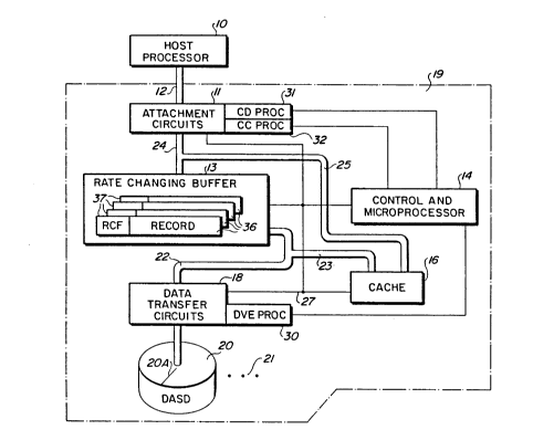
Fig. 1 is a simplified block diagram of a data processing
system employing the present invention.
Fig. 2 is a simplified diagrammatic showing of a record
control field used in the Fig. 1 illustrated system.
Fig. 3 is a simplified system machine operation flow chart
showing the operations used in illustrating the present
invention for the Fig. 1 illustrated system.
Fig. 4 is a simplified machine operations chart for a read
operation showing another application of the present
invention.
Fig. 5 is a simplified machine operations chart showing the
sequence of operations for a recording or a write operation.
Detailed Description an Illustrated Illustrative Embodiment
Referring now more particularly to the appended drawing,
like numerals indicate like parts and structural features in
the various diagrams. Host processor 10 is connected to
peripheral subsystem 19 by a channel connection 12 (Fig. 1).
Connection 12 between host processor 10 and the peripheral
subsystem 19 is is a high speed optical fiber channel 12.
Optical fiber channel 12 can have a relatively long signal
propagation time, i.e., host processor 10 is physically
displaced from the illustrated subsystem by a significant
distance, such as set forth in the Background of the
Invention. A plurality of host processors 10 can be
connected to a single subsystem 19 and correspondingly a
plurality of subsystems 19 can be connected to one or more
TU9-90-010 6
-
204670~
host processors 10. Attachment circuits 11 contain the
usual channel attachment circuits for a peripheral subsystem
19 for enabling communication between the host processor 10
and the peripheral subsystem 19. Included in a controller
portion of the peripheral subsystem 19 is rate changing
buffer 13 for accommodating differences in data burst rates
of the optical fiber channel 12 and DASD s 20 a control and
microprocessor 14 (hereafter microprocessor) and a cache 16,
preferably having a capacity of 100 or more megabytes, which
stores or caches data for a more rapid access by host
processor 10, as is well known. Data transfer circuits 18
are those electronic circuits used to modulate the signals
to be recorded on DASD 20, demodulate signals received from
DASD 20, provide error detection and correction operations
on such data, add and delete control characters and fields,
as is known for such DASD operations. Operation of data
transfer circuits 18 is synchronous with the rotation of a
disk in DASD 20 which is currently being accessed. Each
peripheral subsystem 19 generally will contain a plurality
of DASD s 20 as indicated by ellipsis 21. Each of the data
storage disks (not separately shown) have an index or
reference circumferential position 20A.
Data bus 24 contains control and data lines for enabling
attachment circuits 11 to communicate with rate changing
buffer 13 and has an extension 25 to cache 16 such that
signals from host processor 10 can be received both from
data buffer 13 or cache 16. During a write or recording
operation, the data signals can be supplied only to cache 16
or only to rate-changing buffer 13. The bus 22 connects
rate-changing buffer 13 to data-transfer circuits 18 with a
side bus-connection 23 to cache 16 such that signals from
rate-changing buffer 13 can be recorded on DASD 20 and
simultaneously copied to cache 16. Data read from DASD 20
is supplied to either or both the rate changing buffer 13
and cache 16. Control line 27 represents a plurality of
electrical connectors extending between control and
microprocessor 14, hereafter microprocessor, and other major
TU9-90-010 7
2046709
elements 11, 13, 16 and 18 of the controller for subsystem
19 .
Microprocessor 14 includes a dispatcher or an executive
which manages the operation of the microprocessor for
controlling the peripheral data subsystem, as is known and
practiced. Some of the microcode modules are used
exclusively for providing specific functions involving the
data transfers as will be described for an understanding the
practice of the present invention. Microcode module DVE
PROC 30 shown logically, as being next to data transfer
circuits 18, actually resides physically in the
microprocessor 14, is at portion of the controller
microprocessor 14 for managing the data transfer circuits 18
and for effecting the data transfer operations between DASD
20, rate changing buffer 13 and cache 16. These types of
operations are well known and not further described for that
reason. Similarly, CD PROC 31 is that microcode module of
operating with microprocessor 14 for controlling the
operation of attachment circuits 11 for transferring datà
signals between host processor 10 and rate changing buffer
13 for transfer to DASD 20. Under DVE PROC 30 control, in a
"branching" write operation, a copy of the data in rate
changing buffer 13 is supplied to DASD 20 is also supplied
over bus extension 23 for storage in cache 16. Microcode
module CC PROC 32 of microprocessor 14 controls data
transfers between host processor 10 and cache 16 which do
not involve rate changing buffer 13 nor DASD 20. Transfers
of signals between host processor 10 and a cache 16 is well
known and not detailed for this reason.
With each record 36 stored in rate changing buffer 13 is a
record control field RCF 37. Referring to Fig. 2, RCF 37 is
shown as having a CD PROC portion field 40 for use during
writing operations which is controlled by CD PROC 31 and
read by DVE PROC 30. RCF 37 is initialized by CD PROC 31 on
a write operation and initialized by DVE PROC 30 on a read
operation. Upon a read operation, flag bytes (not shown)
are set by DVE PROC 30 to inform CD PROC 31 the requirements
TU9-90-010 8
204670q
for the record being transferred and the number of records
remaining in the track to be read. All of these other
controls are of no interest in practicing the present
invention. Setting GOCACHE during a DASD read operation can
be for a host command read at either a breakpoint or track
index or after a write domain has ended and a DASD 20 read
mode is established. In some instances several writing
operations may occur in one host processor 10 defined write
domain. GOCACHE could be set at the end of a one of the
several writing operations which is within the host
processor 10 defined write domain. GOCACHE byte 42 is a
flag set by DVE PROC 30 when a DASD 20 portion of a data
processing operation is a DASD read operation and reaches a
predetermined status such that operations with the DASD 20
are to be interrupted and ensuing operations are preferably
conducted with cache 16. Such a direct connection between
host 10 and cache 16 enables a maximum data transfer rate
over the optical fiber channel 12 while the data transfers
with DASD 20 may be more efficient from a control view but
are slower, i.e., do not maximize the burst rate of optical
fiber channel 12. In the operations conducted at the DASD
20 data transfer rate, and are interrupted or segmented
using the GOCACHE flag, as will become apparent. Field 41
indicates the type of record contained in the record image
within rate changing buffer 13. This is used during read
operations for enabling CD PROC 31 to know what type of
record is being transferred of the CKD format. Four types
of records are used in a constructed embodiment of the
present invention. A first is an index or end of track
location, record zero, a home address record (the latter two
are CKD control records) or a user record. Numeral 43
indicates that RCF 37 contains fields other than that shown
in Fig. 2. The flow charts in Fig.'s 4 et seq a~e directed
toward operation of the illustrated Fig. 1 cont~oller for a
single device 20 which is currently transferring data with a
host processor 10 via attachment circuits ll and channel 12.
It is to be understood that when the controller
simultaneously handles more than one device operation at a
TU9-90-010 9
. ".
204670q
time, a plurality of simultaneous operations may occur, each
relating to a different device 20.
Referring next to Fig. 3, an overall view of machine
operations of the Fig. 1 illustrated data processing system
is shown. Host processor 10 starts a data transfer
operation with an address to one DASD 20 at machine step 50.
The data t~ansfer actually occurs between the host processor
and the data processing subsystem at machine step 51. This
step includes transferring data between the DASD 20, the
host processor 10 and between the DASD 20 and cache 16 upon
a read operation and between host processor 10 and cache 16
on a write operation. In machine step 52, DVE PROC 30
monitors the status of the data transfer operation with
respect to DASD 20. The purpose of this monitoring is to
determine a status in which the mode of operations that
switch from device oriented operation to cache oriented
operation for more effectively using the high speed channel
12. At machine step 53, DVE PROC 30 detects a predetermined
end of DAsD operations and sets GOCAC~E flag 42 for
indicating to the rest of the controller a host cache
operation is to ensue. Machine step 54 represents that the
cache-to-host mode is set which is indicated by the CD PROC
31, DVE PROC 30 being inactive, and CC PROC 32 being
established for effecting the data transfers. Activating CC
PROC 32 before it is needed reduces channel response time
between the controller and the host processor 10.
Fig. 4 shows a read operation which uses the present
invention for controlling the data transfers. A read
operation involves asynchronous operations controlled by CD
PROC 31 for transferring data from buffer 13 to host
processor 10 and by DVE PROC 30 for transferring data from
DASD 20 to buffer 13 and cache 16. The DVE PROC 30
operations are first described. A host command read
operation is initiated by host processor 10 at machine step
60, i.e., the controller 19 may have received a read
operation command and is starting DVE PROC 30 to requested
data from DASD 20 to buffer 13 and cache 16. S~ch reading
TU9-90-010 10
-
2046709
is also initiated by controller 19 for desired records. The
operation is described for a host requested read. This read
operation can be for one or more records stored on DASD 20.
At each DVE PROC 30 controlled machine step 61 iteration,
the controller 19 reads one of the host requested data
records from a DASD 20 to buffer 13 and cache 16 for
supplying same via buffer 13 as controlled by CD PROC 31 to
the host processor 10. At the end of each record, DVE PROC
30 determines whether or not an index mark 20A on the track
of Fig. 1 has been sensed. If an index mark 20A is sensed,
then the scanning of the disk is at an end of a track being
addressed, also called a current track. At machine step 63,
DVE PROC 30 determines whether or not the next track is
stored entirely in cache 16. Note that the next track
accessed by host processor 10 can be the current track or
another track. If yes, then at machine step 64 the GOCACHE
flag 42 is set to the active condition for signaling to CD
PROC 31 to send a channel command retry to host processor 10
and to transfer control 10 CC PROC 32. Operation of a
channel co~mand retry (CCR) is well known and not further
described for this reason. Following setting GOCACHE flag
42, DVE PROC 30 stops device operations as indicated at
machine step 65 and waits for another device operation to
begin. If the entire contents of the next track being read
was not stored in cache 16 at machine step 63, then machine
operations return to step 61. As described in the
Background of the Invention, a break point can be the
beginning and end of a roll mode track read operation for
DASD 20 or the location of a first record of a split track
stored in cache. If the break point has been read, then the
contents of the current track being read is in cache and
steps 64 and 65 are then performed. However, if no break
point has been reached, then the read operation should
continue by repeating steps 61, et seq. The operation of
steps 64 and 65 stops the device operation based upon
reaching an index mark and finding the contents of the
current track and cache or reaching a break point during a
read operation. If a next track is to be read and a copy of
data stored in such next track is in cache 16, then the
TU9-90-010 11
. 2046709
machine operations are then shifted from cache-to-host
processor 10 operations for effecting higher data transfer
rates enabled by the connection 12. It is to be understood
that host processor 10 can terminate the Fig. 4 illustrated
machine operations at any time, as is known.
The CD PROC 31 operations which occur asynchronously to the
just-described DVE PROC 30 operations are next described.
CD PROC 31 determines when a host processor 10 read command
has resulted in records stored in buffer 13 are to be
transferred over channel 12 to the host processor. The GET
OP line 90 represents such determination. At machine step
91 a read operation of transferring data from buffer 13 to
host processor 10. At machine step 92, CD PROC 31 checks
the GOCACHE flag 42. If GOCACHE flag 42 is off, then data
is to be transferred, i.e. such as one data record, from
buffer 13 to host processor 13. This data transfer occurs
at machine step 93. Following this data transfer, CD PROC
31 gets identification of the next operation to be
performed, if the next operation is a host processor
commanded read, then steps 91 et seq are repeated, otherwise
operations beyond the scope of the present description are
performed. If at step 91, the GOCACHE flag 42 is ON, then
DVE PROC 30 has indicated that device operations should stop
and cache operations should be initiated. At machine step
95, CD PROC 31 and DVE PROC 30 activities are stopped (note
that reading of DASD 20 has already stopped and this action
deactivates the DVE PROC module) and CC PROC 32 is activated
for initiating cache 16 to host processor 10 data transfers.
CD PROC is exited at 96.
A write operation using the present invention is illustrated
in Fig. 5. At machine step 70, host processor 10 issues a
"LOCATE RECORD" command. This command is a known command
which sets an address space or write domain of DASD 20
address space for limiting the write operation. A write
command follows the LOCATE RECORD command at machine step
71. The data transfers indicated by the write command 71,
which can be for more than one CKD record, is effected at
TU9-90-010 12
2046709
machine step 72. At machine step 73, whether or not the end
of the write domain has been reached is checked. If not, an
additional write command can be received at step 71. This
description assumes that the issued write commands are such
that there is no overrun in rate changing buffer 13 and that
cache 16 has sufficient data storage space for all of the
data to be written to DASD 20. In the event of a possible
overrun, a control mechanism beyond the description of the
present invention can issue a channel command retry (CCR)
which interrupts the transfer of data signals from host
processor 10 to the illustrated data processing subsystem to
prevent overrun or to recover from an overrun error. Such
overrun prevention and recovery is not pertinent to an
understanding of the present invention. If the end of the
write domain has been reached, i.e., writing is completed,
then at machine step 74 a check is made whether or not a
cache hit was made, i.e., was there data in the cache
relating to the write command, if not, device read mode
operations are entered at step 75. If a cache hit has
occurred, i.e., data was in the cache 16 that was
overwritten by the write command, at machine step 72, then
at machine step 76 whether or not a copy of the entire track
is in cache 16 is checked. If yes, if an entire track has
been written and it is in cache, then the GOCACHE flag is
set at step 77. On the other hand, if the entire track is
not in cache, then at machine step 78, whether or not the HA
record is valid is checked, i.e., was index passed, and the
home address record has been stored in cache 16. If yes
then at machine step 78 device read mode operations of step
75 are entered.
While the invention has been particularly shown and
described with reference to preferred embodiments thereof,
it will be understood by those skilled in the art that
various changes in form and details may be màde therein
without departing from the spirit and scope of the
invention.