Language selection

Search

Patent 2046711 Summary

Third-party information liability

Some of the information on this Web page has been provided by external sources. The Government of Canada is not responsible for the accuracy, reliability or currency of the information supplied by external sources. Users wishing to rely upon this information should consult directly with the source of the information. Content provided by external sources is not subject to official languages, privacy and accessibility requirements.

Claims and Abstract availability

Any discrepancies in the text and image of the Claims and Abstract are due to differing posting times. Text of the Claims and Abstract are posted:

  • At the time the application is open to public inspection;
  • At the time of issue of the patent (grant).
(12) Patent: (11) CA 2046711
(54) English Title: MULTILAYER OPTICALLY VARIABLE ELEMENT
(54) French Title: ELEMENT MULTICOUCHE A EFFETS OPTIQUES VARIABLES
Status: Deemed expired
Bibliographic Data
(51) International Patent Classification (IPC):
  • G03H 1/18 (2006.01)
  • B32B 27/08 (2006.01)
  • G03H 1/02 (2006.01)
(72) Inventors :
  • KAULE, WITTICH (Germany)
(73) Owners :
  • GAO GESELLSCHAFT FUR AUTOMATION UND ORGANISATION MBH (Germany)
(71) Applicants :
  • GAO GESELLSCHAFT FUR AUTOMATION UND ORGANISATION MBH (Germany)
(74) Agent: RICHES, MCKENZIE & HERBERT LLP
(74) Associate agent:
(45) Issued: 2002-04-09
(22) Filed Date: 1991-07-10
(41) Open to Public Inspection: 1992-01-11
Examination requested: 1998-06-29
Availability of licence: N/A
(25) Language of filing: English

Patent Cooperation Treaty (PCT): No

(30) Application Priority Data:
Application No. Country/Territory Date
P 40 21 908.9 Germany 1990-07-10

Abstracts

English Abstract


In a multilayer optically variable element, preferably a
hologram, comprising an adhesive layer covered by an easily
removable cover layer, and at least one layer having the
optically variable effect, the protective layer is designed
as a self-supporting and dimensionally stable layer with a
thickness of a few micrometers.


Claims

Note: Claims are shown in the official language in which they were submitted.


8
1. A multilayer optically variable transfer material
having an adhesive layer (22), at least one layer (16, 18,
20) having the optically variable effect, at least one
protective layer (14) and a removable carrier layer (10),
characterized in that the protective layer (14) is designed
as a self-supporting and dimensionally stable layer having a
thickness of from a few micrometers to about 20 µ, and is a
plastic film being selected from the group consisting of
polycarbonate (PC), polyvinyl fluoride (PVF), polyethylene
terephthalate (PETP), polychlorotrifluoroethylene (PCTFE)and
tetrafluoroethylene/hexafluoropropylene copolymer (FEP).
2. The optically variable transfer material as defined in
claim 1 wherein the optically variable transfer material is
a hologram.
3. The optically variable transfer material as defined in
claim 1 or 2 wherein the adhesive layer (22) is covered by
an easily removable cover layer (24).
4. The optically variable transfer material as defined in
any one of claims 1, 2 and 3, characterized in that the
layer with the optically variable effect consists of an
embossed layer (16), a reflective metal layer (18) and a
protective layer (20) that is adjacent to the adhesive layer
(22).
5. The optically variable transfer material as defined in
any one of claims 1, 2 and 3, characterized in that the
layer with the optically variable effect consists of a
photosensitive layer with a volume hologram and further
consisting of a black backing layer covering the
photosensitive layer and adjacent to the adhesive layer
(22), the photosensitive layer being selected from the group


9
consisting of a photosensitive emulsion and a photosensitive
polymer.
6. The optically variable transfer material of claim 5,
characterized in that the black backing layer is formed of
the adhesive layer (22).
7. The optically variable transfer element as defined in
any one of claims 1 to 6, characterized in that the adhesive
layer (22) is a layer of hot-melt adhesive.
8. The optically variable transfer material as defined in
any one of claims 1 to 6, characterized in that the adhesive
layer (22) is a layer of contact adhesive.
9. The optically variable transfer material as defined in
any one of claims 1 to 8, characterized in that contours of
an element to be transferred to a substrate are punched out
or prepunched in the protective layer (14).
10. The optically variable transfer material as defined in
any one of claims 1 to 8, characterized in that it is
present in the form of one selected from the group of an
endless, reelable thread and an endless reelable strip.
11. A substrate with the optically variable transfer
material as defined in any one of claims 1 to 10 glued
thereto.
12. The substrate of claim 11, characterized in that it is
a paper of value.
13. The substrate of claim 12, characterized in that the
paper of value is a bank note.


10
14. The substrate of claim 12 or 13, characterized in that
the optically variable transfer material is glued to the
paper of value in the form of a thread running from edge to
edge.
15. A method for producing an optically variable transfer
material, characterized by the following steps:
a) applying a separation layer (12)to a long-wearing
and machinable carrier film (10),
b) applying a transparent, self-supporting,
dimensionally stable protective film (14) with a
thickness of from a few micrometers to about 20 µ to
the separation layer (12), the protective film (14)
consisting of a plastic film being selected from the
group consisting of polycarbonate (PC), polyvinyl
fluoride (PVF), polyethylene terephthalate (PETP),
polychlorotrifluoroethylene (PCTFE) and
tetrafluoroethylene/hexafluoropropylene copolymer
(FEP),
c) coating the film (14) with an embossable layer of
lacquer (16),
d) embossing a hologram into the layer of lacquer,
e) metalizing the embossed layer of lacquer with a
thin reflective metal layer (18),
f) applying a protective layer (20) covering the
metal layer (18), and


11
g) applying an adhesive layer (22).
16. A method for producing an optically variable transfer
material, characterized by the following steps:
a) applying a separation layer (12) to a long-wearing
and machinable carrier file (10),
b) applying a transparent, self-supporting,
dimensionally stable protective film (14) with a
thickness of from a few micrometers to about 20 µ to
the separation layer (12), the protective film (14)
consisting of a plastic film being selected from the
group consisting of polycarbonate (PC), polyvinyl
fluoride (PVF), polyethylene terephthalate (PETP),
polychlorotrifluoroethylene (PCTFE) and
tetrafluoroethylene/hexafluoropropylene copolymer
(FEP),
c) coating the film (14) with one selected from the
group consisting of a photographic emulsion and a
photopolymer,
d) incorporating a volume hologram into the one
selected from the group consisting of the emulsion and
the photopolymer by appropriate exposure steps,
e) covering the one selected from the group
consisting of the emulsion and the polymer with a black
backing layer, and
f) applying an adhesive layer (22).


12
17. The method as defined in claim 15 wherein the optically
variable transfer material is a hologram.
18. The method as defined in claim 15 or 17, characterized
in that the separation layer (12) is a detachable adhesive
layer.
19. The method as defined in any one of claims 15, 17 and
18, characterized in applying a detachable protective layer
(24).
20. The method as defined in claim 16, characterized in
that the optically variable transfer material is a hologram.
21. The method as defined in claim 16 or 20, characterized
in that the separation layer (12) is a detachable adhesive
layer.
22. The method as defined in any one of claims 16, 20 and
21, characterized in applying a detachable protective layer
(24).
23. The method as defined in any one of claims 16 and 20 to
22, characterized in that the adhesive layer is colored
black.
24. The method as defined in any one of claims 15 to 23,
characterized in that the adhesive layer (22) consists of
contact adhesive that is covered by an easily removable
cover layer (24).
25. The method as defined in claim 24 characterized in that
the easily removable cover layer (24) is silicone paper.


13
26. The method as defined in any one of claims 15 to 25,
characterized in that contours of an element to be
transferred to a substrate are prepunches in the protective
film (14).
27. The method as defined in any one of claims 15 to 23 and
25, characterized in that the adhesive layer (22) comprises
a hot-melt adhesive.
28. The method of any one of claims 15, 16, 23, 24, 26 and
27, characterized in that the optically variable transfer
material is cut into narrow endless threads and wound up.
29. A method for applying an optically variable element
using the transfer material of claim 10 to a substrate,
characterized in that the one selected from the group
consisting of the thread and the strip is wound off a supply
reel (38), the one selected from the group consisting of the
thread and the strip is brought together in a roll slit with
a substrate, the one selected from the group consisting of
the thread and the strip sticks with its adhesive layer to
the substrate, and the carrier film (10) is simultaneously
removed from the one selected from the group consisting of
the thread and the strip upon leaving the roll slit.
30. A method for applying an optically variable element
using the transfer material of claim 9 to a substrate,
characterized in that the substrate and a flat piece of the
optically variable transfer material with the prepunched
area are placed together, the prepunched contour is
subjected to a die, and the flat piece is removed from the
substrate, the prepunched area of the transfer material
sticking to the substrate as an optically variable element.


14
31. The method as defined in claim 30, characterized in
that the die is heated.
32. The method of claim 30 or 31, characterized in that the
optically variable element adhering to the substrate is
again pressed onto the substrate over the entire surface.
33. The method as defined in claim 24,characterized in that
the easily removable cover layer (24) is removed.
34. The method as defined in claim 29 or 33, characterized
in that the substrate is a continuously supplied paper of
value.
35. The method as defined in claim 32, characterized in
that the optically variable element adhering to the
substrate is pressed onto the substrate under the action of
heat after removal of the non-prepunched areas.

Description

Note: Descriptions are shown in the official language in which they were submitted.


CA 02046711 2001-O1-29
A multilayer optically variable element
The present invention relates to a multilave=
optically variable e:ie~ment, preferably a hologram. It aisc
relates to a substrate equipped with the optically variable
element and to a method for producing the optically
variable element.
Optically variables elements are primarily understood to
be holograms and diffraction grids, but they may also be
other elements having an optically visible effect that
changes in accordance with the viewing angle and/or irradi-
ated wavelength due to characteristic interference effects,
reflection, transmission, absorption and other properties.
Holograms are customarily produced in the form of sheet-
like labels and transferred to the desired substrate, such as
paper, plastic, textile material or the like, by means of a
contact adhesive or a hot embossing transfer technique. It is
also known to emboss holograms directly into layers of lac-
quer disposed on the substrate. The holograms are hardened
after embossing by exposure to UV light or electron beams.
Holograms are increasingly used as authenticity features
for protecting papers of value and cards employed in cashless
money transfer. Such holograms must firstly be tamper-=esist-
ant, i.e. virtually undetachable from the carrier. Further-
more, they must withstand considerable mechanical stresses
over a long time without showing any noticeable changes.
Holograms consisting of plastic films affixed to a sub-
strate with a contact adhesive have relatively high stabili-
ty, i.e. they are most suitable for withstanding the mechani-
cal stresses that arise. A disadvantage, however, is their
thickness and the resulting rigidity, that makes it impossi-
ble to employ such adhesive labels for protecting bank notes,
for example.


CA 02046711 2001-O1-29
2
Holograms that are embossed into a thin layer of lacquer
disposed on the substrate can be used in many ways, for exam-
ple in bank notes due to their small thickness. However, the
layer of lacquer is very sensitive to mechanical and chemical
stresses. They are therefore unsuitable for protecting papers
of value and cards which are used daily for some time.
German laid open patent application publication DE-OS
33 08 831 published on May 10,1984 discloses a hologram
that can be applied to a substrate by the transfer method.
To permit better hand7_ing of the relatively thin hologram
it is connected by a reparation layer with a relatively
stable carrier film that can be removed after the hclogram
has been applied to the substrate. This technique permits
the application of relatively thin-layer holograms that can
hardly be handled as ~~uch due tc their low dimensional
stability and rigidit~T. This property is utilized to rule
out a subsequen- detachment of the hologram for purposes of
manipulation. On the other hand, the hologram can be
machined together with the carrier film, for example,
brought together with a substrate i~: a roll slit.
The known hologram has on its side facing away from the
carrier film a hot-melt adhesive layer permitting labels to
be transferred to a substrate, their contour corresponding
exactly to the contour of a heated die with which the com-
pound material is pressed against the substrate. After the
carrier layer is detached the known hologram is protected by
a thermoplastic transparent layer that has no dimensional
stability and is not self-supporting so as to prevent detach-
ment. This thermoplastic protective gayer does not impede the
transfer to the substrate in any way since it tears in the
edge area of the heated transfer die when the carrier film
is removed after the hologram has been pressed onto the sub-
strate, thus also permitting easy detachment of those areas
which are not loaded by the transfer die. However, it must be
regarded as a serious disadvantage that this thermoplastic
protective layer is relatively soft and unresistant. A holo-
gram protected with such a layer does not withstand mechani-


CA 02046711 2001-O1-29
3
cal and chemical environmental influences for any length of
time.
The present invention is based on the problem of provid-
ing an optically variable element that has minimal thickness
while being maximally resistant to environmental influences,
i.e. to abrasion, crumpling, soiling, washing, chemicals,
etc., and that is easy to produce, on the one hand, while
being transferable to a substrate without difficulty by means
of a transfer method, on the other hand.
This problem is sclved according to the invention
which resides in providing multilayer optically variable
element having an adhesive layer (22), at least one layer
(16, 18, 20) having the optically variable effect, at least
one protective layer (14) and a removable carrier layer
(10), characterized in that the protective layer (14) is
designed as a self-supporting and dimensionally stable
layer having a thickness of from a few micrometers t-o about
20 ~.
The invention is based on the finding that the hologram
can in fact be mechanically unstable for security reasons but
the protective layer of the hologram must not be an unstable,
non-self-supporting film but rather a layer that withstands
mechanical loads to a maximal degree despite its small thick-
ness. A particularly suitable film has proven to be one made
of PC, PVF, PETP, PCTFE or FEP with a thickness of from a few
micrometers to about 20 u, in particular in the range of 10
u. Since such thin films cannot be handled by machines the
film compound is combined, in the basically known way, with a
carrier film that is r~amoved after the hologram has been
applied to the substrate.
When holograms are .applied the contour of the particular
plane element is prepun~~hed in the thin protective film, so
that it is readily posaible to detach or extract the hologram
from the surrounding m<~teriai.


CA 02046711 2001-O1-29
3a
Replacing the known unstable layer by an equally thin but
extremely resistant film, for example of polycarbonate (PC),
polyvinyl fluoride (PVF), polyethylene terephthalate (PETP),
polychlorotrifluoroet:hylene (PCTFE), tetrafluoroethylene/
hexafluoropropylene copolymer (FEP), together with the meas-
ure of prepunching th~~ hologram contours, results in a holo-


_~ ,
4 ,
gram that combines in an unprecedented way the advantages of
particularly small thickness with the advantages of excellent
mechanical durability. With consideration of possible securi-
ty aspects the layer supporting the hologram should be dimen-
sioned without any great inherent strength, while the protec-
tive film should be selected in terms of thickness and mate-
rial properties such that when applied to the substrate it
can sufficiently protect the hologram layer from mechanical
and other loads, on the one hand, but is dimensioned such
that subsequent detachment leads at least to an irreversible
deformation or destruction, on the other hand. A protective
film of PC, PVF, PETP, PCTFE or FEP, in a thickness of about
3 to 20 N, in particular in the range of 10 N, meets these
basically contradictory demands excellently. If sufficiently
viscous plastics material is used, a layer thickness of about
1 (~ is even possible. Furthermore, such a hologram can be
applied to a substrate either as an adhesive label or by
known heat-sealing techniques. If protection from forgery is
of less interest the embossed structure can also be incorpo-
rated directly into.the protective layer. In this case the
further hologram layer can be omitted.
Instead of an embossed hologram one can of course also
use other layers with optically variable effects, for example
a photographic emulsion layer with a volume hologram, a dif-
fraction grid or a layer with interference or color change
effects.
To fabricate the compound film material the material is
most simply cut into strips and rolled up. These strips or
threads are preferably applied to an continuously supplied
substrate in a calender-like roller frame.
For label-like holograms of any desired contour the basi-
cally known decal technique is applied, i.e. the label con-
tour is prepunched into the thin protective film so that the
label sticks to the substrate when the carrier film is re-
moved.


5
Due to their mechanical stability under load and their
small thickness, the inventive holograms are particularly
suitable for equipping papers of value such as bank notes.
Furthermore, the easy handling and inexpensive production of
the transfer material are of great importance.
In the following some embodiment examples of the inven-
tion shall be described by way of example with reference to
the adjoined drawing. in which:
Figs. 1a to c show various production steps for the
transfer material,
Fig. 2 shows schematically the production of the transfer
material of Fig. 1a, and
Fig. 3 shows schematically the application of a hologram
to an endless paper strip.
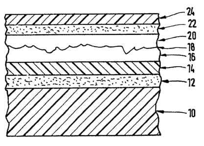
The inventive hologram shown in Figs. 1a to 1c comprises
a relatively thick, stable carrier film 10. Polyester films
are preferably used. The carrier film bears a separation
layer 12, for example a wax, that ensures easy removal of
carrier film 10 from the rest of the compound material. Adja-
cent to separation layer 12 is transparent thin protective
film 14 which is preferably made of PC, PVF, PETP, PCTFE or
FEP. Such films are known for their excellent mechanical
durability and dimensional stability. Protective film 14
bears an embossed layer 16 which consists far example of a
known embossable lacquer. The embossed lacquer relief is
customarily metalized. The metalizing is suggested in Figs.
1b and 1c by reference number 18.
The reflective metal layer may bear a protective layer 20
which is followed by an adhesive layer 22. Protective layer
20 can also be omitted; under certain circumstances it may
suffice for sufficiently thick adhesive layer 22 to lie di-
rectly on embossed hologram 18.

i
~,~ . .... .. . .... .t
6
If the adhesive layer is a contact adhesive, i.e, an
adhesive that sticks in the cold state, the adhesive layer
must be covered with a layer 29 to permit handling of the
compound material. Silicone paper has proven particularly
useful in this connection. If the layer is a hot-melt adhe-
sive, such a paper layer is of course unnecessary since the
hot-melt adhesive only develops its adhesive effect at
higher temperatures.
Instead of embossed hologram 18 one can also provide a
photosensitive layer into which the hologram is incorporated
by exposure, i.e. a so-called volume hologram. Such photosen-
sitive layers and their treatment axe known; suitable materi-
als are photopolymers or fine-grained photographic emulsions.
The volume hologram is covered, not with a metal layer, but
with a black backing layer of lacquer. It is also possible to
color the already existing adhesive layer 22 black.
The production of a semifinished product according to
Fig. 1a is shown schematically in Fig. 2. A separation layer
(release layer) made of wax, for example, is applied at 28 to
carrier film 10 unrolled from a drum 26. The inventive pro-
tective film runs from a film producing or unrolling means 30
to laminating means 32 in which the film is laminated to the
carrier film by passing through a roll slit. Embossed layer
16 is then applied in unit 34. The compound material accord-
ing to Fig. 1a is finally wound onto drum 36 and subsequently
processed in the known way.
The further steps are the embossing of a hologram into
embossed layer 16, the vacuum metalizing of embossed layer 1.6
before or after embossing, and then optionally the applica-
tion of a protective layer 20. The adhesive, which may be a
contact adhesive or a hot-melt adhesive, is then applied to
the protective layer. If a contact adhesive is used the com-
pound material is covered with silicone paper.
Fig. 3 shows the schematic diagram of an application sys-


CA 02046711 2001-O1-29
7
tem for applying the holograms to an endless paper strip. The
film compound materia=~ according to Fig. lc is removed from
drum 38, whereby silicone paper 24 is first detached from the
compound material via drum 40. The paper to be provided with
the hologram is suppl~_ed from drum 42 to a roller frame 44,
whereupon the hologram is pressed with contact adhesive layer
22 onto the paper in a roll slit. The paper with the~hologram
adhering thereto is wound onto drum 46 while the carrier film
is detached from the compound and runs to drum 48. In the
case shown a continuous hologram strip or endless thread is
transferred to the paper carrier.
It is of course likewise possible to work with the known
hot transfer technique, i.e. to design adhesive layer 22 as a
heat-sealing layer an~i emboss the hologram on by means of
rolls or heated dies. This means that only the adhesive layer
located directly below the roll or die softens and adheres to
the substrate. Upon removal, all parts of the compound mate-
rial are also removed which were located in areas not heated
by the die.
When using island7.ike labels it is of course necessary,
regardless of the adhesive method used (hot-melt adhesive,
contact adhesive, etc..;~, to accordingly prepunch thin pro-
tective film 14, which is a tear-resistant, stable material,
since it is otherwise impossible to extract the hologram
label from the film compound. Preferably, the optically
variable elements adhering to the substrate are again
pressed on to the sub;~trate over the entire surface and
optionally under the action of heat after removal of the
non-prepunched areas


CA 02046711 2001-O1-29
7a
Further layers ca.n of course also be present in the ele-
ment in addition to the described layers, for example to pro-
vide protection from forgery. It is also conceivable to pre-
treat the paper carrier so as to improve adhesion o~ the
smoothness of the transition. Such measures are e.g. the pre-
vious application of adhesive layers or bonding agents to the
paper, or the preembo;ssing or glazing of the paper in the
areas where the hologram is to be disposed:~

Representative Drawing
A single figure which represents the drawing illustrating the invention.
Administrative Status

For a clearer understanding of the status of the application/patent presented on this page, the site Disclaimer , as well as the definitions for Patent , Administrative Status , Maintenance Fee  and Payment History  should be consulted.

Administrative Status

Title Date
Forecasted Issue Date 2002-04-09
(22) Filed 1991-07-10
(41) Open to Public Inspection 1992-01-11
Examination Requested 1998-06-29
(45) Issued 2002-04-09
Deemed Expired 2011-07-10
Correction of Expired 2012-12-02

Abandonment History

There is no abandonment history.

Payment History

Fee Type Anniversary Year Due Date Amount Paid Paid Date
Application Fee $0.00 1991-07-10
Registration of a document - section 124 $0.00 1992-12-11
Maintenance Fee - Application - New Act 2 1993-07-12 $100.00 1993-06-25
Maintenance Fee - Application - New Act 3 1994-07-11 $100.00 1994-07-05
Maintenance Fee - Application - New Act 4 1995-07-10 $100.00 1995-07-05
Maintenance Fee - Application - New Act 5 1996-07-10 $150.00 1996-06-10
Maintenance Fee - Application - New Act 6 1997-07-10 $150.00 1997-06-25
Request for Examination $400.00 1998-06-29
Maintenance Fee - Application - New Act 7 1998-07-10 $150.00 1998-06-30
Maintenance Fee - Application - New Act 8 1999-07-12 $150.00 1999-06-30
Maintenance Fee - Application - New Act 9 2000-07-10 $150.00 2000-04-13
Maintenance Fee - Application - New Act 10 2001-07-10 $200.00 2001-03-29
Final Fee $300.00 2002-01-21
Maintenance Fee - Patent - New Act 11 2002-07-10 $200.00 2002-07-05
Maintenance Fee - Patent - New Act 12 2003-07-10 $200.00 2003-05-05
Maintenance Fee - Patent - New Act 13 2004-07-12 $450.00 2004-07-21
Maintenance Fee - Patent - New Act 14 2005-07-11 $250.00 2005-06-17
Maintenance Fee - Patent - New Act 15 2006-07-10 $450.00 2006-06-19
Maintenance Fee - Patent - New Act 16 2007-07-10 $450.00 2007-06-19
Maintenance Fee - Patent - New Act 17 2008-07-10 $650.00 2008-07-28
Maintenance Fee - Patent - New Act 18 2009-07-10 $450.00 2009-06-30
Owners on Record

Note: Records showing the ownership history in alphabetical order.

Current Owners on Record
GAO GESELLSCHAFT FUR AUTOMATION UND ORGANISATION MBH
Past Owners on Record
KAULE, WITTICH
Past Owners that do not appear in the "Owners on Record" listing will appear in other documentation within the application.
Documents

To view selected files, please enter reCAPTCHA code :


To view images, click a link in the Document Description column. To download the documents, select one or more checkboxes in the first column and then click the "Download Selected in PDF format (Zip Archive)" or the "Download Selected as Single PDF" button.

List of published and non-published patent-specific documents on the CPD .

If you have any difficulty accessing content, you can call the Client Service Centre at 1-866-997-1936 or send them an e-mail at CIPO Client Service Centre.


Document
Description 
Date
(yyyy-mm-dd) 
Number of pages   Size of Image (KB) 
Abstract 2001-09-04 1 10
Claims 2001-09-04 7 207
Description 2001-01-29 9 343
Drawings 1994-03-30 3 50
Claims 2001-10-03 7 210
Representative Drawing 2001-10-15 1 16
Claims 2001-01-29 7 209
Cover Page 1994-03-30 1 18
Abstract 1994-03-30 1 12
Claims 1994-03-30 5 152
Description 1994-03-30 7 324
Cover Page 2002-03-20 1 34
Prosecution-Amendment 2000-08-08 2 76
Fees 2000-04-13 1 38
Prosecution-Amendment 2001-09-04 12 320
Prosecution-Amendment 2001-10-03 6 161
Prosecution-Amendment 2001-11-06 2 54
Assignment 1991-07-10 7 249
Prosecution-Amendment 1998-06-29 1 41
Prosecution-Amendment 2001-01-29 17 510
Correspondence 2002-01-21 1 38
Prosecution-Amendment 2001-03-05 2 68
Fees 1997-06-25 1 42
Fees 2001-03-29 1 38
Fees 2002-07-05 1 35
Fees 1998-06-30 1 46
Fees 1999-06-30 1 37
Fees 1995-07-05 1 42
Fees 1996-06-10 1 40
Fees 1994-07-05 1 47
Fees 1993-06-25 1 35