Note: Descriptions are shown in the official language in which they were submitted.
20~72~1
RADIO COMMUNICATION APPARATUS WHICH CAN BE
TESTED BY RADIO AND OPTICAL TEST SIGNALS
Background of the Invention:
This invention relates to a radio communication
apparatus for use in combination with a test transmitter
for use in testing the radio communication apparatus.
This invention relates also to the test transmitter for
transmitting a radio test signal carrying a test digital
data signal. The radio communication apparatus may be a
radio paging receiver, a transceiver, or the like
although description will be mainly made in connection
with the radio paging receiver.
A test transmitter of the type described,
generally comprises a signal producing section for
producing the test digital data signal. Connected to the
signal producing section, a radio test signal
transmitting section transmits the radio test signal
which carries the test digital data signal.
A radio paging receiver of the type described,
generally comprises a radio processing section for
2 20~72~1
processing the radio test signal into the test digital
data signal. Supplied with the test digital data signal
as an input digital data signal, a data processing
section processes the input digital data signal into a
processed data signal. Connected to the data processing
section, an announcing section carries out an announcing
operation of generation of the processed data signal in
response to the processed data signal.
On testing the radio paging receiver, the test
transmitter transmits to the radio paging receiver the
radio test signal carrying the test digital data signal.
When the radio paging receiver has not a faulty
component, the announcing section announces generation of
the processed data signal. When the radio paging
receiver has a faulty component, the announcing section
does not announce generation of the processed data
signal. Thus, the radio paging receiver can be tested or
judged as regards whether or not the radio paging
receiver has a faulty component.
However, when it is judged that the radio paging
receiver has the faulty component, it is difficult to
specify whether the faulty component is the radio
processing section or a remaining part comprising the
data processing section and the announcing section.
Summary of the Invention:
It is therefore an object of this invention to
provide a radio communication apparatus operable in
combination with a test transmitter, wherein a faulty
2047251
component can easily be specified.
It is another object of this invention to provide
a radio communication apparatus of the type described,-
wherein it is easily judged whether the faulty component
is a radio processing section or a remaining section.
It is a further object of this invention to
provide a test transmitter for use in combination with a
radio communication apparatus, which test transmitter
makes it easy to specify a faulty component in the radio
communication apparatus.
Other objects of this invention will become clear
as the description proceeds.
On describing the gist of an aspect of this
invention, it is possible to understand that a radio
communication apparatus is for use in combination with a
test transmitter for use in testing the radio
communication apparatus. The test transmitter is for
transmitting a radio test signal carrying a test digital
data signal. The radio communication apparatus includes:
radio processing means for processing the radio test
signal into the test digital data signal; data processing
means supplied with an input digital data signal for
processing the input digital data signal into a processed
data signal; and announcing means connected to the data
processing means for carrying out an announcing operation
of generation of the processed data signal in response to
the processed data signal.
According to this aspect of this invention, ~he
,~ .
- 4 2047251
above-understood radio communication apparatus
comprising: optical processing means supplied with an
optical test signal carrying the test digital signal that
is transmitted by the test transmitter, the optical
processing means being for processing the optical test
signal into the test digital data signal; and selecting
means connected to the radio and the optical processing
means and to the data processing means for selecting one
of the test digital data signals produced by the radio
and the optical processing means. The selecting means
produces the above-mentioned one of the test digital data
signals as the input digital data signal.
On describing the gist of a different aspect of
this invention, it is possible to understood that a test
transmitter is for use in testing a radio communication
apparatus. The test transmitter includes: signal
producing means for producing a test digital data signal;
and radio test signal transmitting means for transmitting
a radio test signal carrying the test digital data
signal. The radio communication apparatus includes:
radio processing means for processing the radio test
signal into the test digital data signal; data processing
means supplied with an input digital data signal for
processing the input digital data signal into a processed
data signal; and announcing means connected to the data
processing means for carrying out an announcing operation
of generation of the processed data signal in response to
the processed data signal.
..~
2047251
According to the different aspect of this
invention, the above-understood test transmitter
comprises: optical test signal transmitting means for
transmitting an optical test signal carrying the test
digital data signal; and selective supplying means
connected to the signal producing means and to the radio
and the optical test signal transmitting means for
selectively supplying the test digital data signal to one
of the radio and the optical test signal transmitting
means. The radio communication apparatus comprises:
optical processing means for processing the optical test
signal into the test digital data signal; and selecting
means connected to the radio and the optical processing
means and to the data processing means for selecting one
of the test digital data signals produced by the radio
and the optical processing means. The selecting means
produces, as the input digital data signal, the
above-mentioned one of the test digital data signals
produced by the radio and the optical processing means.
Brief Description of the Drawing:
Fig. 1 is a block diagram of a combination of a
radio paging receiver according to a first embodiment of
this invention, a test transmitter, and a base station;
Fig. 2 is a signal format for use in describing
operation of the radio paging receiver illustrated in
Fig. l;
Fig. 3 is a block diagram of a radio paging
receiver according to a second embodiment of this
6 2`047251
nventlon;
Fig. 4 is a block diagram of a part of a modified
example of the radio paging receiver illustrated in Fig. 3;
Fig. 5 is a flow chart for describing operation
of the modified example illustrated in Fig. 4;
Fig. 6 is a block diagram of a radio paging
receiver according to a third embodiment of this
invention; and
Fig. 7 is a view for use in describing a test
method for testing the radio paging receiver illustrated
in Fig. 6.
Description of the Preferred Embodiments:
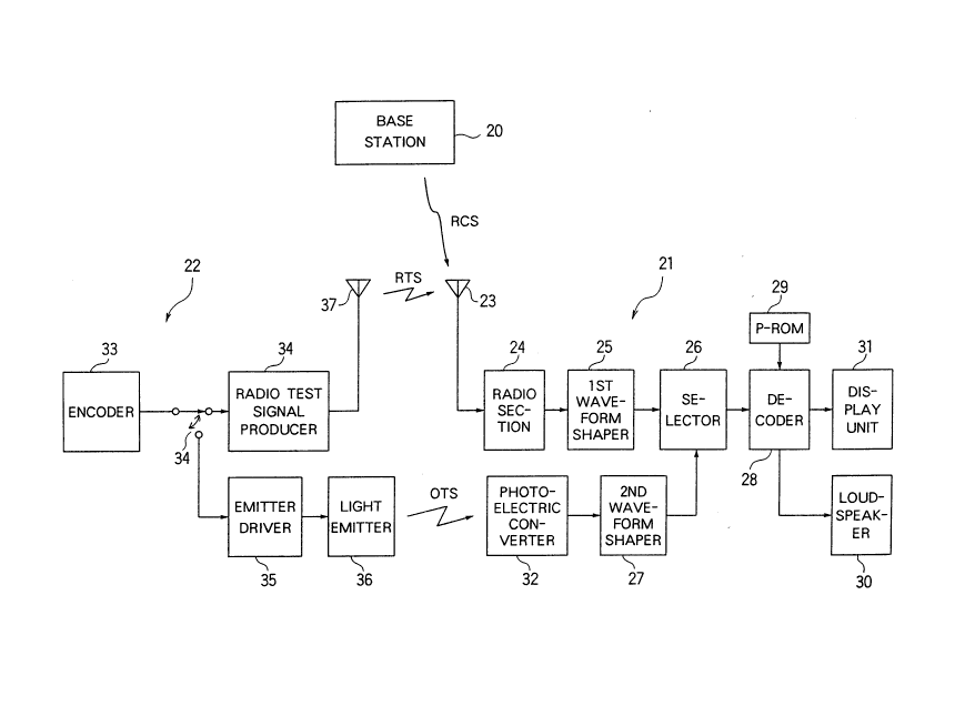
Referring to Fig. 1, a radio paging system
comprises a base station 20, a radio paging receiver 21
according to a first embodiment of this invention, and
other radio paging receivers (not shown) which are
similar in structure and in operation to the radio paging
receiver 21. The base station 20 is for transmitting a
radio communication signal indicated at RCS. The radio
paging receiver 21 deals with the radio communication
signal RCS in the manner which will become clear as the
description proceeds.
The radio paging receiver 21 is for use in
combination with a test transmitter 22 which is for use
in testing the radio paging receiver 21. The test
transmitter 22 is usually carried by a maintenance
engineer who is in charge of maintenance service of the
radio paging system. The test transmitter 22 is fc~
-
7 20~7251
transmitting a radio test signal indicated at RTS.
Turning to Fig. 2, the radio communication signal
RCS is illustrated along a top or first line. The
illustrated radio communication signal RCS is a POGSAG
code radio signal which is set up in CCIR recommendation
584. The radio communication signal RCS comprises a
plurality of frames which are similar in frame structures
tb one another.
Each frame of the radio communication signal RCS
carries a synchronization signal SYN and first through
n-th subframes SFl to SFn successively succeeding the
synchronization signal SYN, where n represents an integer
greater than one. The synchronization signal SYN has a
predetermined number of bits and is specified by a
predetermined pattern of bits.
The radio paging receiver 21 (Fig. 1) and other
radio paging receivers of the radio paging system have
call numbers different from one another and may be
grouped into first through n-th groups. The first
through the n-th groups are assigned to the first through
the n-th subframes SFl to SFn of each frame,
respectively. Supposing that the radio paging receiver
21 belongs to the first group, the base station 20 (Fig.
1) transmits a call number signal CN representative of
the radio paging receiver 21 and a communication message
signal CME representative of a communication message
directed to the radio paging receiver 21 by using the
first subframe SFl The call number signal CN has a
- 2047251
preselected number of bits. The communication message
signal CME has another preselected number of bits. Each
of the synchronization signal SYN, the call number signal
CN, and the communication message signal CME consists of
Bose-Chaudhuri-Hocquenghem tBCH) codes.
A combination of the synchronization signal SYN,
the call number signal CN, and the communication message
signal CME will be referred to herein as a communication
digital data signal. The communication data signal is
carried by the radio communication signal RCS.
In Fig. 2, the radio test signal RTS is
illustrated along a second line. The radio test signal
RTS is similar in frame structure to the radio
communication signal RCS except that the call number
signal CN representative of the radio paging receiver 21
and a test message signal TME representative of a test
message are transmitted by using the first through the
N-th subframes SFl to SFn in order to test the radio
paging receiver 21. Alternatively, the call number
signal CN and the test message signal TME may be
transmitted by using only the first subframe SFl.
A combination of the synchronization signal SYN,
the call number signal CN, and the test message signal
TME is referred to herein as a test digital data signal.
The test digital data signal is carried by the radio test
signal RTS.
Turning back to Fig. 1 with reference to Fig. 2
continued, description will be made as regards operation
c, ~
9 2047251
of the radio paging receiver 21 when the radio paging
receiver 21 is tested by the test transmitter 22. In
this event, the maintenance engineer makes the test
transmitter 22 transmit the radio test signal RTS at
first.
The radio test signal RTS LS picked up by an
antenna 23 and supplied to a radio section 24. The radio
section 24 converts or demodulates the radio test signal
RTS into a baseband or demodulated signal. Connected to
the radio section 24, a first waveform shaper 25 shapes
the demodulated signal into a shaped signal of a digital
waveform. The shaped signal has the test digital data
signal (namely, a combination of the synchronization
signal SYN, the call number signal CN, and the test
message signal TME).
Thus, a combination of the antenna 23, the radio
section 24, and the first waveform shaper 25 serves as a
radio processing section for processing the radio test
signal RTS into the test digital data signal.
A selector 26 is connected to the first waveform
shaper 25 and a second waveform shaper 27 which will
later be described. In the manner which will become
clear as the description proceeds, the selector 26 is
made by the maintenance engineer so as to select, as a
selected signal, the test digital data signal produced by
the first waveform shaper 25.
Supplied with the selected signal as an input
digital data signal, the decoder 28 d~tects the
X
20~7251
synchronization signal SYN in order to establish bit
synchronization and frame synchronization. After the bit
synchronization and the frame synchronization are
established, the decoder 28 cooperates with a P-ROM
(programmable read-only memory) 29 which preliminarily
memorizes a directory number signal indicative of a
directory number assigned to the radio paging receiver
21. That is, the decoder 28 compares the call number
signal CN with the directory number signal bit by bit.
When the decoder 28 detects coincidence between
bits of the call number signal CN and the directory
number signal, the decoder 28 sends a speaker drive
signal to a loudspeaker 30 to make the loudspeaker 30
generate a call tone indicative of a call to the radio
paging receiver 21 a predetermined time duration.
Simultaneously, the decoder 28 sends the test message
signal TME to a display unit 31 to make the display unit
31 visually display the test message of the test message
signal TME. The display unit 31 is, for example, a
liquid crystal display (LCD).
Thus, the decoder 28 serves, in cooperation with
the P-ROM 29, as a data processing section supplied with
the input digital data signal. The data processing
section processes the input digital data signal into a
processed data signal (namely, the speaker drive signal
and the test message signal TME ) . A combination of the
loudspeaker 30 and a display unit 31 serves as an
announcing section connected to the data processing
-
ll 2047251
section. The announcing section carries out an
announcing operation of generation of the processed data
signal in response to the processed data signal.
When the radio paging receiver 21 carries out
generation of the call tone and display of the test
message while the test transmitter 22 transmits the radio
test signal RTS, the maintenance engineer judges that the
radio paging receiver 21 has not a faulty component.
When the radio paging receiver 21 carries out
neither generation of the call tone nor display of the
test message in spite of transmission of the radio test
signal RTS from the test transmitter 22, the maintenance
engineer judges that the radio paging receiver 21 has a
faulty component. In this case, the maintenance engineer
makes the test transmitter 22 transmit an optical test
signal OTS instead of the radio test signal RTS in order
to judge whether the faulty component is the radio
processing section or a remaining part comprising the
data processing and the announcing sections.
The optical test signal OTS carries the test
digital data signal like the radio test signal RTS. More
specifically, the optical test signal OTS is controlled
or modulated by the test digital data signal to form a
flicker light which indicates logic "1" and "0" levels of
the test digital data signal.
A photoelectric converter 32 converts the optical
test signal OTS into a converted or demodulated signal.
Connected to the photoelectric converter 32, the second
g
12 2047251
waveform shaper 27 shapes the converted signal into a
shaped signal of a digital waveform that is equivalent to
the test digital data signal (namely, a combination of
the synchronization signal SYN, the call number signal
CN, and the test message signal TME).
Thus, a combination of the photoelectric
converter 32 and the second waveform shaper 27 is
operable as an optical processing section which processes
the optical test signal OTS into the test digital data
slgnal.
In the manner which will become clear as the
description proceeds, the selector 26 is now made by the
maintenance engineer so as to select, as the selected
signal, the test digital data signal produced by second
waveform shaper 27. As described above, the decoder 28
is supplied with the selected signal as the test digital
data signal.
Thus, the selector 26 is connected to the radio
and the optical processing section and to the data
processing section (namely, a combination of the decoder
28 and the P-ROM 29) to select one of the test digital
data signals produced by the radio and the optical
processing sections. The selector 26 produces the
above-mentioned one of the test digital data signals as
the input digital data signal of the data processing
section.
When the radio paging receiver 21 carries out
generation of the call tone and display of the test
g
13 2047251
message while the test transmitter 22 transmits the
optical test signal OTS, the maintenance engineer judges
that the faulty component is the radio processing
section.
When the radio paging receiver 21 carries out
neither generation of the call tone nor display of the
test message in spite of transmission of the optical test
signal OTS from the test transmitter 22, the maintenance
engineer confirms, by the use of a measuring instrument
of, for example, a voltmeter or an oscilloscope, whether
or not the test digital data signal is present in a first
connection point between the second waveform shaper 27
and the selector 26. Subsequently, the maintenance
engineer confirms, by the use of the measuring
instrument, whether or not the test digital data signal
is present in a second connection point between the
selector 26 and the decoder 28. When the maintenance
engineer confirms that the test digital data signal is
present in the first connection point and that the test
digital data signal is present in the second connection
point, the maintenance engineer judges that the faulty
component is the remaining part (namely, a combination of
the data processing section and the announcing section).
When the radio paging receiver 21 has not a
faulty component, the radio paging receiver 21 is
operable in response to the radio communication signal
RCS in the manner similar to a case where the radio
paging receiver 21 receives the radio test signal RTS.
g
14 2047251
In this event, the loudspeaker 30 generates the call tone
when the radio paging receiver 21 receives the call
number signal CN representative of the call number
assigned to the radio paging receiver 21. The display
unit 31 displays the communication message of the
communication message signal CME when the radio paging
receiver 21 receives the communication message signal CME
which succeeds the call number signal CN representative
of the call number assigned to the radio paging receiver
21.
Attention will proceed to the test transmitter
22. The test transmitter has an encoder 33 which serves
as a signal producing section for producing the test
digital data signal having logic "1" and "O" levels. A
transmitter switch 34 selectively supplies the test
digital data signal to one of a radio test signal
producer 35 and an emitter driver 35 for driving a light
emitter 36 which is, for example, an LED (light-emitting
diode), a laser diode, or the like.
When supplied with the test digital data signal
through the transmitter switch 34, the radio test signal
producer 34 produces the radio test signal RTS carrying
the test digital data signal. The radio test signal RTS
is transmitted through an antenna 37.
Thus, a combination of the radio test signal
producer 34 and the antenna 37 is operable as a radio
test signal transmitting section which transmits the
radio test signal RTS carrying the test digital data
2~17251
signal.
When supplied with the test digital data signal,
the emitter driver 35 produces an on-off drive signal
which indicates on and off when the test digital data
signal has logic "1" and "0" levels, respectively.
Responsive to the on-off drive slgnal, the light emitter
36 emits or transmits the flicker light as the optical
test signal OTS carrying the test digital data signal.
Thus, a combination of the emitter driver 35 and
the light emitter 36 serves as an optical test signal
transmitting section which transmits the optical test
signal OTS carrying the test digital data signal. The
transmitter switch 34 serves as a selective supplying
section connected to the signal producing section
(namely, encoder 33) and to the radio and the optical
test signal transmitting sections. The selective
supplying section selectively supplies the test digital
data signal to one of the radio and the optical test
signal transmitting sections.
Turning to Fig. 3, a radio paging receiver
according to a second embodiment of this invention
comprises similar parts designated by like reference
numerals. The radio paging receiver comprises an
illuminator 39, such as a lamp, connected to the decoder
2B. The illuminator 39 illuminates the display unit 31
by illuminating light when the illuminator 39 is driven
by the decoder 28.
The selector 26 comprises a switch 40 havinc
- 20472~1
16
negative and positive terminals connected to the earth or
ground directly and a voltage source through a resistor
41, respectively. The voltage source is indicated at +V
and gives a positive voltage to the positive terminal.
The negative terminal is supplied with an earth voltage.
It will be assumed that the positive and the earth
voltages corresponding to a logic "0" level and a logic
"1" level.
The switch 40 is usually put in an off state.
That is, the switch 40 is put in the off state when the
radio test signal RTS is transmitted by the radio
transmitter 22 (Fig. 1). The switch 40 is put in an on
state by the maintenance engineer when the optical test
signal OTS is transmitted by the test transmitter 22.
Description will be made as regards operation of
the selector 26 when the switch 40 is put into the off
state. In this case, a first AND circuit 42 is supplied
with the logic "1" level through the resistor 41.
Inasmuch as an inverter 43 is supplied with the logic "1"
level through the resistor 41 and inverts the logic "1"
level into the logic "0" level, a second AND circuit 43
is supplied with the logic "0" level. The first AND
circuit 42 thereby delivers to an OR circuit 45 the test
digital data signal produced by the first waveform shaper
25. The OR circuit 45 delivers to the decoder 28 the
test digital data signal produced by the first waveform
shaper 25.
A third AND circuit 46 is supplied with the logic
17 2047251
"1" level through the resistor 41. Inasmuch as an
inverter 47 is supplied with the logic "1" level through
the resistor 41 and inverts the logic "1" level into the
logic "0" level, a fourth AND circuit 48 is supplied with
the logic "0" level. The third AND circuit 46 thereby
delivers to the decoder 28 an output signal of the second
waveform shaper 27.
Attention will be directed to the photoelectric
converter 32. The photoelectric converter 32 comprises a
phototransistor 50 having a collector and an emitter
connected to the earth or ground. The collector is
connected to the voltage source +V through a resistor 51.
The phototransistor 50 is supplied with
environment light of the radio paging receiver when the
test transmitter 22 does not transmit the optical test
signal OTS but transmits the radio test signal RTS. When
the environment light has a high intensity or brightness,
a collector voltage of the collector of the
phototransistor 50 becomes nearly equal to an earth
voltage. When the environment light has a low intensity
or brightness, the collector voltage becomes nearly equal
to the positive voltage of the voltage source +V. Thus,
the collector voltage varies in compliance with an
intensity of the environment light. The photoelectric
converter 32 supplies the collector voltage to the second
waveform shaper 27 as the converted signal.
The second waveform shaper 27 shapes the
converted signal into a shaped signal of a dlgital form.
~~~ 18 204 7251
The shaped signal has a logic "1" level when the
environment light has a low intensity. When the
environment light has a high intensity, the shaped signal
has a logic "0" level. That is, when environment of the
radio paging receiver becomes dark, the shaped signal has
the logic "1" level.
In the manner described above, the third AND
circuit 46 of the selector 26 delivers the shaped signal
(namely, the output signal of the second waveform shaper
27) to the decoder 28 when the switch 40 is put in the
off state. On condition that the decoder 28 receives the
shaped signal of the logic "1" level when the decoder 28
drives the display unit 31 so as to make the display unit
31 display the test message, the decoder 28 drives the
illuminator 39 to make the illuminator 39 illuminate the
display unit 31 by the illuminating light.
Description will proceed to operation of the
selector 26 when the switch 40 is put in the on state.
As mentioned above, the switch 40 is put in the on state
when the optical test signal OTS carrying the test
digital data signal is transmitted by the test
transmitter 22. In this case, the phototransistor 50 is
supplied with the optical test signal OTS rather than the
environment light and processes the optical test signal
OTS into the converted or demodulated signal in the
manner similar to a case where the phototransistor 50 is
supplied with the environment light. The second waveform
shaper 27 shapes the converted signal into the test
g
lg 20~7251
digital data signal.
When the switch 40 is put in the on state, the
earth voltage (namely, the logic "0" level) is supplied
to the inverters 47 and 43 through the switch 40.
Inasmuch as the inverters 47 and 43 supply the fourth and
the second AND circuits 48 and 44 with the logic "1"
level, the test digital data signal is delivered to the
decoder 28 as the input digital data signal through the
fourth and the second AND circuits 48 and 44 and the OR
circuit 45. Inasmuch as the earth voltage (namely, the
logic "0" level) is supplied to the third and the first
AND circuits 46 and 42, output signals of the second and
the first waveform shapers 27 and 25 are not delivered
through the third and the first AND circuits 46 and 42 to
the decoder 28.
Turning to Fig. 4, a transistor switch 52 may be
used instead of the switch 40 illustrated in Fig. 3. The
transistor switch 50 has a base electrode, a collector
electrode, and an emitter electrode connected to the
earth. The collector electrode is connected to the
resistor 41, the inverters 43 and 47, and the third AND
circuit 46 like the positive terminal of the switch 40.
In order to put the transistor switch 52 in one
of off and on states, a logic circuit 53 is connected to
the base electrode of the transistor switch 52. The
logic circuit is also connected to an output of the
second waveform shaper 27. When the maintenance engineer
wishes to put the transistor switch 52 in the off state,
~~ 20 2047251
the maintenance engineer makes an optical signal
generator (not shown) generate a first optical signal
towards the phototransistor 50 under a dark environment
in which the environment light of the radio paging
receiver is cut off. The first optical signal carries an
off signal having a first predetermined pattern. When
the maintenance engineer wishes to put the transistor
switch 52 in the on state, the maintenance engineer makes
the optical signal generator generate a second optical
signal under the dark environment. The second optical
signal carries an on signal having a second predetermined
pattern that is different from the first predetermined
pattern. The first and the second optical signals may be
transmitted by the test transmitter 22 (Fig. 1).
Turning to Fig. 5, the first optical signal is
illustrated at OFF SIG along a first or top line. The
first optical signal has a first part which is shown at
(a) and which is a dark part continuing for T seconds. A
second part succeeds the first part (a) and is shown at
(b). Bright and dark parts alternately appears at a
first period in the second part (b) in a predetermined
period.
The second optical signal is illustrated at ON
SIG along a second line. The second optical signal has a
preceding part which is shown at (c) and is substantially
equivalent to the first part (a) of the first optical
signal. A succeeding part succeeds the preceding part
(c) and is shown at (d). Bright and dark parts
`~~ 21 20472~1
alternately appears in the succeeding part (d) at a
second period which is different from the first period.
Turning back to Fig. 4, a combination of the
phototransistor 50, the resistor 51, and the second
waveform shaper 27 processes the first and the second
optical signals into the off and the on signals of
electric waveform when the phototransistor 50 is supplied
with the first optical signal and when the
phototransistor 50 is supplied with the second optical
signal, respectively.
When the logic circuit 53 receives the off
signal, the logic circuit 53 continuously produces the
logic "O" or low level (namely, the earth voltage) until
the logic circuit 53 receives the on signal. Supplied
with the low level, the transistor switch 52 is put in
the off state. When the logic circuit 53 receives the on
state, the logic circuit 53 continuously produces the
logic "1" or high level until the logic circuit 53
receives the off signal.
Turning to Fig. 6, a radio paging receiver
according to a thlrd embodiment of this invention
comprises similar parts designated by like reference
numerals. The radio paging receiver comprises a power
source 55 having an on state and an off state. The power
source switch 55 is connected to a battery 56 which
serves as a power source. When the power source switch
55 is put in the on state, each part of the radio paging
receiver is supplied with an electric power from the
22 20~7251
battery 56.
Description will be made on the supposition that
the power source switch 55 is put in the on state and
that each part of the radio paging receiver is supplied
with the electric power. Further supposing that the
radio paging receiver receives the radio test signal RTS
(Fig. 2). In this case, the decoder 28 detects
coincidence between bits of the call number signal CN of
the test digital data signal and the directory number
signal. When the decoder 28 detects the coincidence, the
decoder 28 produces a coincidence signal representative
of the coincidence. Subsequently, the decoder 28
produces the test message signal TME which succeeds the
call number signal CN of the test digital data signal.
A first switch 57 is manually operable and has an
on state and an off state. The first switch 57 is
connected to the earth or ground which will be referred
to as a reference voltage source.
A second switch 58 is manually operable and has
an on state and an off st~te. The second switch 58 is
connected to the earth.
A controller 59 is connected to the decoder 28,
the first and the second switches 57 and 58, and a
message memory 60 which may be an RAM (random access
memory). In a case where the controller 59 receives the
coincidence signal when the first switch 57 is put in the
off state, the controller 59 sends a speaker drive signal
to the loudspeaker 30 through a speaker driver 61 to make
23 204 725I
the loudspeaker 30 generate the call tone. In another
case where the controller 59 receives the coincidence
signal when the first switch 57 is put in the on state,
the controller 59 does not send the speaker drive signal
to the loudspeaker 30 to inhibit generation of the call
tone.
Responsive to the coincidence signal, the
controller 59 stores in the message memory 60 the test
message signal TME succeeding the call number signal CN.
In a case where the controller 59 receives the test
message signal TME when the second switch 58 is put in
the off state, the controller 59 sends the test message
signal TME to the display unit 31 through a display
driver 62 to make the display unit 31 display the test
message. In another case where the controller 59
receives the test message signal CME when the second
switch 58 is put in the on state, the controller 59 does
not send the test message signal TME to the display unit
31 to inhibit display of the communication message.
Thus, a combination of the controller 59, the
message memory 60, the speaker driver 61, and the display
driver 62 serves as a controlling section connected to
the data processing section (namely, a combination of the
decoder 28 and the P-ROM 29) and to the first and the
second switches 57 and 58. The controlling section
controls the announcing section (namely, a combination of
the loudspeaker 30 and the display unit 31) to permit the
announcing operation when the first switch 57 (or the
24 2047251
second switch 58) is put in the off state. When the
first switch 57 (or the second switch 58) is put in the
on state, the controlling section controls the announcing
section to inhibit the announcing operation.
A first transistor switch 63 has a base electrode
(namely, a control terminal) and on and off states and
connected to the first switch 57 in parallel. The first
transistor switch 63 is controllably put in the on state
when the base electrode is supplied with a predetermined
control voltage. The predetermined control voltage is
substantially equivalent to a logic "1" level.
A second transistor switch 64 is connected to the
second switch 58 in parallel and is similar in structure
and in operation to the first transistor switch 63. Each
of the first and the second transistor switches 63 and 64
will be referred to as an electrically controllable
switch.
The optical processing section (namely, a
combination of the photoelectric converter 32 and the
second waveform shaper 27) is supplied with an optical
control signal carrying a digital control signal that is
transmitted by the test transmitter 22 (Fig. 2). The
optical processing section processes the optical control
signal into the digital control signal.
A decoder 65 is connected to the second waveform
shaper 27 through a switching circuit 66 which will later
be described. In the manner which will become clear as
the description proceeds, the switching circuit 66
g
204 7251
supplies the digital control signal to the decoder 65.
The decoder 65 decodes the digital control signal into a
decoded signal of the logic "1" level and supplies the
decoded signal to the control terminal of at least one of
the first and the second transistor switches 63 and 64.
The above-mentioned at least one of the first and the
second transistor switches 63 and 64 is determined by the
digital control signal.
Thus, the decoder 65 serves as a control signal
processing section connected to the optical processing
section and to the control terminal. The control signal
processing section processes the digital control signal
into the predetermined voltage (namely, a logic "1"
level) and supplies the control terminal with the
predetermined voltage.
Referring to Figs. 6 and 7, description will
proceed to a test method for testing the radio paging
receiver illustrated in Fig. 6. On testing the radio
paging receiver, the maintenance engineer puts the power
source switch 55 in the on state. When the power source
switch 55 is put in the on state, each part of the radio
paging receiver is supplied with the electric power from
the battery 56. When the power source switch 55 is put
in the on state, a trigger signal is produced by a
differentiating circuit having capacitor 67 and a
resistor 68. Responsive to the trigger signal, the
controller 59 continuously supplies a switching
instruction signal to the switching circuit 66. Supplied
26 20472Sl
with the switching instruction signal, the switchlng
circuit 66 connects an output of the second waveform
shaper 27 to an input of the decoder 65 and maintains
this connecting state while the switching instruction
signal is received.
When the maintenance engineer makes the test
transmitter 22 transmits an optical start signal carrying
a digital test start signal. The optical processing
section (namely, photoelectric converter 32 and second
waveform shaper 27) processes the optical start signal
into the digital test start signal. When the decoder 65
receives the digital test start signal through the
switching circuit 66, the decoder 65 decodes the digital
test start signal into a test start signal and delivers
the test start signal to the controller 59. When the
controller 59 receives the test start signal within a
predetermined time interval after the controller 59
receives the trigger signal, the controller 59
continuously supplies the switching instruction signal
until the controller 59 receives a test end signal. The
test end signal is produced by the decoder 65 when the
decoder 65 decodes a digital test end signal. The
digital test end signal is carried by an optical end
signal transmitted by the test transmitter.
When the controller 59 does not receive the test
start signal within the predetermined time interval, the
controller 59 stops supply of the switching instruction
signal. The switching circuit 66 connects the output of
27 20~ 72~1
the second waveform shaper 27 to an input of the
controller 59 when the switching circuit 66 is not
supplied with the switching instruction signal.
While the switching circuit 66 connects the
output of the second waveform shaper 27 to the input of
the decoder 65, the maintenance engineer makes another
test transmitter (not shown) transmit the radio test
signal RTS carrying the test digital data signal.
Subsequently, the maintenance engineer makes the test
transmitter 22 transmit the optical control signal
carrying the digital control signal.
In Fig. 7, a television camera 69 serves as an
image pickup device for picking up a displayed image of
the display unit 31 to produce an image signal
representative of the displayed image. An image
processor 70 is connected to the television camera 69 for
processing the image signal. A microphone 71 is for
converting the call tone into an electric (voice) signal.
Connected to the microphone 71, a voice processor 72
processes the voice signal.
Turning back to Fig. 6, when the switching
circuit 66 connects the output of the second waveform
shaper 27 to the input of the controller 59, the
photoelectric converter 32 converts the environment light
into an electric signal. The second waveform shaper 27
shapes the electric signal into a shaped signal of a
digital form. The shaped signal is delivered to the
controller 59 through the switching circuit 66. Th~
~,~1
~ 28 204 7251
controller 59 drives the illuminator 39 through an
illuminator driver 73 like the decoder 28 of Fig. 3.
While this invention has thus far been described
in conjunction with a few embodiments thereof, it will
readily be possible for those skilled in the art to put
this invention into practice in various other manners.
In Fig. 6, the controller 59 may send the speaker drive
signal to the loudspeaker 30 when the controller 59
receives the coincidence signal with the first switch 57
put in the on state. In Fig. 6, a microphone may be used
instead of the photoelectric converter 32. In this case,
the test transmitter transmits a voice signal of a
predetermined frequency instead of the optical control
signal in order to put the transmitter switch 63 in the
off state.
c
",~.