Note: Descriptions are shown in the official language in which they were submitted.
21)472~4
.
A DEMODULATOR AND A POLARIZATION DIVERSITY RECEIVER FOR
COHERENT OPTICAL COMMUNICATION PROVIDED WITH THE
DEMODULATOR
BACKGROUND OF TIIE INVENTION
Field of the Invention
The present invention relates to a demodulator
and a polarization diversity receiver for coherent
optical communication provided with the demodulator.
The coherent optical transmission method is
suitable for long-distance transmission because higher
reception sensitivity is obtained thereby than that
obtained by the intensity-modulation/direct-detection
method in practical use today. Further, since frequency
selection can be achieved relatively easily by
electrical processing after optical detection has been
made, it is suitable for transmission by frequency-
division multiplexing at a high density. Now, since -the
term "detection" is liable to be confused with the term
"demodulation", the term "detection" or "optical
detection" herein will be used to mean the conversion
from an optical signal to an electrical signal
(intermediate-frequency signal) and the term
2047284
"demodulation" will be used to mean the conversion from
an intermediate-frequency signal to a baseband signal.
When signal reception is performed through
heterodyne detection, it is required in mixing the
signal light with the local light that the polarization
state of both of the light beams is in agreement.
Disagreement between the polarization states leads to
deterioration in the reception sensitivity. When, for
example, both the signal light and the local light are
linearly polarized light and the planes of polarization
are orthogonal to each other, there is produced no
interference on the photodetecting surface and hence the
signal reception becomes unachievable. Since single
mode fibers in general are not capable of retaining the
1~ polarized state, the polarized state on the receiving
end varies due to changes in the environmental
conditions with time. Therefore, in order to maintain a
required reception sensitivity, it becomes necessary to
cope with the variation in the polarization state on the
receiving end.
Description of the Related Art
As a technique to cope with the variation in
the polarization state on the receiving end, there is a
~0`472~4
polarization diversity system. A prior art e~ample of
structure of a polarization diversity receiver for
coherent optical communication to which such system is
applied is shown in FIG. 19. Reference numeral l11
denotes an optical local oscillator made up of a
semiconductor laser or the like. This optical local
oscillator 111 outputs local light having a frequency in
a specific relation with the frequency of the received
signal light. Reference numeral 112 denotes an
optical/electrical converter made up of polarization
beam splitters, optical couplers, optical detecting
circuits, and the like in combination. The converter 112
performs optical/electrical conversion of the received
signal and the local light for each of the polarization
components, of which the planes of polarization are
orthogonal to each other, to thereby output two
intermediate frequency signals (IF signals), for each of
the polarization components, having the frequency
corresponding to the difference between the frequency of
the signal light and the frequency of the local light.
One of the IF signals is input to a demodulator 115
through variable gain amplifiers 113 and 114, and the
other IF signal is separately input to a demodulator 118
through variable gain amplifiers 116 and 117.
~0172~4
.
Demodulated signals from the demodulators are
respectively passed through variable gain amplifiers 119
and 120 and added together in an adder 121 and then
input to a discriminator 122 whereby the transmitted
information is regenerated. Reference numeral 123
denotes a control circuit for controlling gains in each
of the variable gain amplifiers and reference numeral
124 denotes an automatic frequency control circuit for
controlling the frequency of the local light so that the
frequency of the IF signal may be kept constant.
The manner of the gain controlling operation
performed in the control circuit 123 will be described
below. Total power of the received signal light in
general varies with conditions of the light transmission
path and the like. Now, we represent the power of the
signal light by k. Since the -two IF signals output from
the optical/electrical converter 112 are based on the
polarization components of the signal light having
planes of polarization orthogonal to each other, the
ratio of power between the two IF signals becomes a : (1
- a), where 0 _ a < 1. Therefore, the power of the IF
signal input from the optical/electrical converter 112
to the variable gain amplifier 113 is proportional to
ka, and the power of the IF signal input from the
20472~4
optical/electrical converter 112 to the variable gain
amplifier 116 is proportional to k(1 - a). The variable
gain amplifiers 113 and 116 are for coping with
variation in the power of the signal light and the
amplification factor of them is controlled to be
proportional to k-1. The term "amplification" herein
includes the case where the amplification factor is less
than unity, i.e., it includes attenuation. The power of
the IF signal output from the variable gain amplifier
113 is rid of the effect of the variation in the total
power of the signal light and, hence, is made
proportional to a and the power of the IF signal output
from the variable gain amplifier 116 is rid of the
effect of the same variation and, hence, is made
proportional to (1 - a). The variable gain amplifiers
114 and 117 are for equalizing the power of the IF
signals input to the demodulators 115 and 118. Hence,
the amplification factor of the variable gain amplifier
114 is controlled to be proportional to a~1 and the
amplification factor of the variable gain amplifier 117
is controlled to be proportional to (1 - a)~1, whereby
the power of the IF signals input to the demodulators
115 and 118 are made equal. The variable gain
amplifiers 119 and 120 are for weighting the input
~0~728~
signal so as to obtain a weighted sum by, for example,
the maximum ratio combining law. These amplifiers 119
and 120 perform amplification of the input signals at
amplification factors proportional to the S/N ratio or
the signal power of the input signal. More
specifically, since the power of the IF signals input to
the demodulators 115 and 118 are controlled to be equal
in the present example, the amplification factor of the
variable gain amplifier 119 is set to be proportional to
aZ, while the amplification factor of the variable gain
amplifier 120 is set to be proportional to (1 - a)Z.
A prior art example of structure of the
demodulator is shown in FIG. 20. This demodulator is
made up of a branch circuit 130, such as a 3 dB coupler,
for providing branch outputs of the input signal, a
delay circuit 131 for delaying one of the output signals
of the branch circuit 130 by a predetermined delay time
and output-ting the delayed signal, and a mul~iplier 132
for multiplying the other of the output signals of the
branch circuit 130 and the output signal of the delay
circuit 131 together.
As described above, the prior art demodulator
was a combination of analog circuits and therefore it
has not always been easy to form them in a monolithic
~0~7284
integrated circuit structure.
Further, since the prior art demodulator shown
in FIG. 20 is an analog circuit using a multiplier
(mixer) and the like, it sometimes fails to perform a
normal demodulating operation unless the level of the
input to the demodulator is held constant. Because of
this, in the prior art polarization diversity receiver
for coherent optical communication, it was required to
provide variable gain amplifiers 114 and 117, as shown
in FIG. 19, for holding the power of the IF signals
input to the demodulators. Thus, the circuit requires
to have at least six variable gain amplifiers in all and
a controlling circuit therefor. Therefore, the prior
art polarization diversity receiver has had a
disadvantage that its structure is complex.
In order to simplify the structure of the
polarization diversity receiver, an arrangement in which
a variable gain amplifier for coping with the variation
in the IF signal due to the power variation in the
signal light (for example, the variable gain amplifier
113) and a variable gain amplifier for controlling the
power of the IF signal input to the demodulator to be
constant tfor example, the variable gain amplifier 114)
are unified is proposed. In such case, however, the
204728~
28170-21
dynamlc range of the galn controlllng clrcult for the unlfied
varlable galn ampllfler is required to be hlgher than 30 dB, and
therefore, the proposed arrangement ls dlfflcult to be practlcally
reallzed.
SUMMARY OF THE INVENTION
An ob~ect of the present lnventlon ls to provlde a
modulator uslng digital clrcuit elements and sultable for being
formed lnto a monollthlc lntegrated clrcult.
Another ob~ect of the present lnventlon is to provide a
polarlzatlon dlversity recelver for coherent optlcal communlcatlon
using the above mentloned modulator and having a smaller number of
varlable galn amplifiers and therefore is slmpler ln structure of
the controlllng circuit.
According to a broad aspect of the invention there is
provlded a demodulator ln an optlcal recelver for demodulatlng a
modulated optlcal signal, cornprising: an OR/NOR circuit having an
lnput port supplled wlth an lntermedlate-frequency slgnal obtalned
from the modulated optical slgnal and a first and a second output
port, adapted such that, when the input level at sald lnput port
is at a low level, output levels of sald first and second output
ports are respectively brought to a low level and a hlgh level
and, when the input level at said input port ls at a high level,
output levels of sald flrst and second output ports are
respectlvely brought to a hlgh level and a low level; a delay
clrcult for delaylng the output slgnal from the second output port
of sald OR/NOR clrcult by a predetermlned delay tlme ~ and
204728~
-
28170-21
outputting the delayed signal; and an e~cluslve OR/NOR clrcult
having a first lnput port supplied with the output signal from the
first output port of sald OR/NOR circuit, a second input port
supplied with the output signal from said delay circuit, and a
first and a second output port from which demodulated slgnals are
output, adapted such that, when input levels at said first and
second input ports are in phase output levels at the first and
second output ports are respectively brought to a low level and a
high level, and when input levels at said first and second input
ports are in antiphase, output levels at said first and second
output ports are respectively brought to a high level and a low
level, the demodulator being for use in a direct modulation phase
shift keying system, in which an ln~ectlon current supplled to a
semlconductor laser, whlch outputs light with a frequency
correspondlng to the ln~ection current, ls varied for a
predetermined modulation time t, which is shorter than one time
slot T of a binary coded input signal, such that the integrated
value of the frequency varied according to the injected current
becomes a phase amount of ~ or -~ said predetermined delay time
being set to a time corresponding to one time slot T of the
modulated slgnal.
According to another broad aspect of the invention there
is provided a demodulator in an optlcal receiver for dernodulating
a modulated optical signal, comprising: an OR/NOR circuit having
an input port supplied with an intermediate-frequency signal
obtained from the modulated optical signal and a first and a
second output port, adapted such that, when the input level at
~B
2047284
-
28170-21
sald lnput port ls at a low level, output levels of sald flrst and
second output ports are respectively brought to a low level and a
hlgh level and, when the input level at said input port is at a
high level, output levels of said first and second output ports
are respectively brought to a high level and a low level, a delay
circult for delaying the output signal frol-n the second output port
of said OR/NOR circuit by a predetermined delay time ~ and
outputting the delayed signal; and an exclusive OR/NOR circuit
having a flrst lnput port supplied with the output signal frorn the
first output port of said OR/NOR circuit, a second input port
supplied wlth the output signal from said delay circuit and a
first and second output port from which demodulated signals are
output, adapted such that, when input levels at said first and
second input ports are in phase, output levels at said first and
second output ports are respectively brought to a low level and a
high level, and when input levels at said first and second input
ports are in antiphase, output levels at said first and second
output ports are respectively brought to a high level and a low
level, wherein said demodulator for use in a continuous phase
frequency shift keying syste~-n, and wherein sald predetermined
delay time ~ is set to ~=T/2m, where m represents the modulation
index expressed as m=~ F/B, where ~ F represents the frequency
shift and B represents the bit rate of the modulated signal, and T
represents one time slot of the modulated signal.
According to another broad aspect of the invention there
is provided a demodulator in an optical receiver for demodulating
a modulated optical signal, comprising: an OR/NOR circuit havlng
~.. ..... , ~
2047284
28170-21
an input port supplled with an intermediate-frequency signal
obtained from the modulated optical signal and a first and a
second output port adapted such that, when the input level at
said input port is at a low level, output levels of said first and
second output ports are respectlvely brought to a low level and a
high level and, when the input level at said input port is at a
high level, output levels of said flrst and second output ports
are respectively brought to a high level and a low level; a delay
circuit for delaying the output signal from the second output port
of said OR/NOR circuit by a predetermined delay time r and
outputting the delayed signal; and an exclusive OR/NOR circuit
having a first input port supplied with the output signal frorn the
first output port of said OR/NOR circuit a second input port
supplied with the output signal from said delay circuit, and a
first and a second output port from which demodulated signals are
output, adapted such that, when input levels at said first and
second input ports are in phase, output levels at said first and
second output ports are respectively brought to a low level and a
high level, and when input levels at said first and second input
ports are in antiphase, output levels at said first and second
output ports are respectlvely brought to a high level and a low
level, wherein said demodulator for use in direct modulation phase
shift keying system, in which an in~ection current supplied to a
semiconductor laser, which outputs light with a frequency
corresponding to the in~ectlon current, is varied for a
predetermined modulation tirne t, which is shorter than one time
slot T of a blnary coded input slgnal, such that the lntegrated
- 204 7284 28170-21
value of the frequency varled accordlng to the lnlected current
becomes a phase amount of n or -~, whereln sald predetermlned
delay time ~ ls set to a time corresponding to one time slot T of
the modulated signal, and wherein said predetermlned modulatlon
tlme t ls set to t=T/2mr where m represents a modulatlon lndex
expressed as m=~F/B, where ~ F represents the frequency shift and
B represents the blt rate of the modulated slgnal, and T
represents one time slot of the modulated signal.
According to another broad aspect of the invention there
is provided a polarization diversity receiver for coherent optical
communication comprising: an optical local oscillator outputting
local light; an optical-electrical converter for performing
optical-electrical conversion of received signal light and said
local llght for each of polarization components, of which planes
of polarization are orthogonal to each other, thereby outputting
two intermediate-frequency signals having the frequency
corresponding to the difference between the frequency of said
signal light and the frequency of said local light, for each of
said polarization components; a first and second demodulator
respectively supplied with said intermediate-frequency signals;
and a combining clrcult for comblnlng demodulated slgnals from
said first and second demodulators; wherein each of said first and
second demodulators comprlses: an OR/NOR circuit having an input
port supplied with the intermedlate-frequency signal and a first
and a second output port and adapted such that, when the input
level at said input port is at a low level, output levels at said
first and second output ports are respectively brought to a low
lla
2047284
28170-21
level and a hlgh level and, when the lnput level at said input
port ls at a hlgh level, output levels at sald flrst and second
output ports are respectlvely brought to a hlgh level and a low
level; a delay clrcuit for delaying the output slgnal from the
second output port of said OR/NOR circuit by a predetermlned delay
tlme ~ and outputting the delayed signal; and an exclusive OR/NOR
clrcult havlng a flrst lnput port supplled wlth the output slgnal
frorn the flrst output port of sald OR/NOR circuit, a second lnput
port supplled wlth the output slgnal from sald delay clrcult, and
a flrst and a second output port outputtlng demodulated slgnals,
and adapted such that, when the lnput levels at sald flrst and
second lnput ports are ln phase, output levels at sald flrst and
second output ports are respectlvely brought to a low level and a
hlgh level and, when the lnput levels at sald flrst and second
lnput ports are ln antlphase, output levels at sald flrst and
second output ports are respectlvely brought to a high level and a
low level.
The above and other objects, features and advantages of
the present inventlon and the manner of reallzing them wlll become
more apparent, and the lnventlon itself will best be understood
from a study of the followlng descrlptlon and appended clalms wlth
reference had to the attached drawings showing sorne preferred
embodlments of the lnventlon.
llb
~..
20472~4
-
28170-21
BRIEF DESCRIPTION OF THE DRAWINGS
FIG. 1 is a block dlagram showing a demodulator
accordlng to the present lnventlon;
FIG. 2 to FIG. 5 are block dlagrams showlng a
- llc
~B
~,
~047284
first to a fourth basic structure of the polarization
diversity receiver for coherent optical communication
according to the present invention;
FIG. 6 is a block diagram showing an example
of structure of the transmitter applicable to a DPSK
system;
FIG. 7 is a block diagram showing an example
of structure of the transmitter applicable to a CPFS~
system;
FIG. 8 is a block diagram showing an example
of structure of the transmitter applicable to a DM-PSK
system;
FIG. 9 is a diagram for explaining the
principle of operation in the DM-PSK system;
FIG. 10 is a diagram for explaining an example
of setting up of driving waveform in the DM-PSK system;
FIG. 11 is a block diagram showing a first
embodiment of the polarization diversity receiver for
coherent optical communication according to the present
invention;
FIG. 12 is a diagram showing an example of
structure of an optical detecting circuit;
FIG. 13 is a diagram showing another example
of structure of an optical detecting circuit (a double
2047284
balanced type);
FIG. 14 is a graph showing an example of
weighting function f(a);
FIG. 15 is a graph showing the dependency on
polarization of deterioration in the reception
sensitivity;
FIG. 16 is a graph showing the relationship
between deterioration in -the reception sensitivity and
dynamic range;
FIG. 17 and FIG. 18 are block diagrams showing
a second and a third embodiment of the polarization
diversity receiver for coherent optical communication
according to the present invention;
FIG. 19 is a block diagram showing a prior art
polarization diversity receiver for coherent optical
communication; and
FIG. 20 is a block diagram showing a prior art
demodulator.
DESCRIPTION OF THE PREFERRED EMBODIMENTS
Preferred embodiments of the present invention
will be described below in detail with reference to the
accompanying drawings.
FIG. 1 is a block diagram showing a
- ~4728q
demodulator according to the present invention.
Reference numeral 1 denotes an OR/NOR circuit realized
as a digital circuit element and it has an input port la
and a first and a second output port lb and lc. The
OR/NOR circuit 1 functions as follows. That is, when
-the input level at the input port la is a low level, the
output levels at the first and second output ports lb
and lc are respectively brought to a low level and a
high level, and when the input level at the input port
la is a high level, the output levels at the first and
second output ports lb and lc are respectively brought
to a high level and a low level.
The truth table of the OR/NOR circuit 1 is
shown in Table 1. Referring to the table, D1 denotes
the level at the input port la, Q1 denotes the level at
the first output port lb, and Q2 denotes the level at
the second output port lc. Numeral "0" in the table
indicates the low level and "1" indicates the high
level.
Table 1 Truth Table of the OR/NOR Circuit 1
Input Signal Q1 Q2
O 0
D1
0
14
~0~7284
Reference numeral 2 denotes a delay circuit
for outputting a delayed signal of the output signal at
the second output port lc of the OR/NOR circuit 1 by a
predetermined delay time r .
Reference numeral 3 denotes an exclusive
OR/NOR circuit realized as a digital circuit element.
The exclusive OR/NOR circuit 3 has a first input port 3a
receiving the output signal of the first output port lb
of the OR/NOR circuit 1, a second input port 3b
receiving the output signal of the delay circuit 2, and
a first and a second output port 3c and 3d. The
exclusive OR/NOR circuit 3 functions as follows. When
-the input levels at the first and second input ports 3a
and 3b are in phase (when the inputs are both at the
high level or both at the low level), the output levels
at the first and second output ports 3c and 3d are
respectively brought to a low level and a high level,
and when the input levels at the first and second input
ports 3a and 3b are in antiphase (when, for example, the
first input port 3a is at a high level and the second
input port is at a low level), the output levels at the
first and second output ports 3c and 3d are respectively
brought to a high level and a low level.
The truth table of the exclusive OR/NOR
2047284
circuit 3 is shown in Table 2. Referring to the table,
Dl and D2 respectively denote the levels at the first
input port 3a and the second input port 3b, Q] denotes
the level at the first output port 3c, and Q2 denotes
the level at the second output port 3d. Numeral "0"
indicates the low level and "1" indicates the high
level.
Table 2 Truth Table of Exclusive OR/NOR Circuit
Input Signal Q1 Q2
(O, O) 0
(O, 1) 1 0
(Dl, D2)
(1, O) 1 0
(1, 1) 0
It is adapted such that an intermediate-
frequency signal is input to the input port la of the
OR/NOR circuit 1 and a demodulated signal is output from
the first output port 3c or the second output port 3d of
the exclusive OR/NOR circuit 3.
In the foregoing, the OR/NOR circuit 1 was
described to be that having one input port. When an
ordinary OR/NOR circuit having two input ports is used,
one input port may always be set to the low level and
16
~047284
,
the other input port may be used as described above.
According to the arrangement shown in FIG. 1,
satisfactory demodulation can be achieved by setting the
delay time ~ in the delay circuit 2 to a value fitted
for the type of modulation as described later.
Generally, in a digital circuit element such
as the OR/NOR circuit 1 and the exclusive OR/NOR circuit
3, the dynamic range is wide. More specifically, the
acceptable range of variation of the input level for
providing the normal operation of the digital circuit
element is wide and, in addition, the output level is
virtually constant. For example, the digital circuit
element can properly operate with the input amplitude
(peak-to-peak) ranging from 0.4 to 1.2V, approximately,
1~ and its output amplitude is constantly around 0.9V.
Therefore, when a polarization diversity receiver for
coherent optical communication is arranged using the
demodulators of the present invention, the variable gain
amplifiers for equalizing the power of IF signals input
to the two demodulators can be eliminated and the
structure of the receiver can be simplified by such
reduction in the number of the gain control loops.
Further, according to the structure of FIG. 1,
a demodulator can be realized by the use of the digital
20472~4
circuit elements and a suitable delay line in
combination. Hence, it can be easily achieved to form
the demodulator in a monolithic IC structure.
FIG. 2 to FIG. 5 are block diagrams showing a
first to a fourth basic structure of the polarization
diversity receiver for coherent optical communication
according to the present invention including the
demodulator as shown in FIG. 1.
Throughout these drawings, the same reference
numerals denote the same objects. Referring to FIG. 2,
reference numeral 11 denotes an optical local oscillator
for outputting local light. Reference numeral 12
denotes an optical-electrical converter, and this
optical-electrical converter 12 performs optical-
electrical conversion of a received signal light, andthe local light, for each of polarization components, of
which planes of polarization are orthogonal to each
other, to thereby output two intermediate-frequency
signals (IF signals) for each of the polarization
components with a frequency corresponding to the
difference between the frequency of the signal light and
the frequency of the local light.
Reference numerals 13 and 14 respectively
denote a first and a second demodulator of the structure
18
~`0~72~
as shown in FIG. 1. These demodulators 13 and 14 are
respectively supplied with the above described
intermediate-frequency signals. Particular examples of
setting up of the delay time in the delay circuit of the
demodulator will be described later.
Reference numeral 15 denotes an adder, which
adds up the signal from the first output port 3c of the
first demodulator 13 and the signal from the first
output port 3c of the second demodulator 14.
In the second basic structure shown in FIG. 3,
the signal from the second output port 3d of the first
demodulator 13 and the signal from the second output
port 3d of the second demodulator 14 are added Up by the
adder 16.
In the third basic structure shown in FIG. 4,
the signal from the first output port 3c of the first
demodulator 13 and the signal from the second output
port 3d of the second demodulator 14 are subjected to
subtraction in the subtractor 17.
In the fourth basic structure shown in FIG. 5,
the signal from the second output port 3d of the first
demodulator 13 and the signal from the first output port
3c of the second demodulator 14 are subjected to
subtraction in the subtractor 18.
19
~047284
According to the first, second, third, or
fourth basic structures of the receiver, the demodulated
signals can be obtained from either or both of the first
and second demodulators even if a variation occurs in
the state of polarization of the signal light.
Therefore, by combining the obtained demodulated signals
by means of the adder or subtractor, reception of the
signal light can be achieved at all times irrespective
of the state of polarization of the signal light.
FIG. 6 is a block diagram showing an e~ample
of structure of a transmitter for coherent optical
communication applicable to a differential phase shift
keying system (DPSK system). Reference numeral 21
denotes a semiconductor laser controlled so as to output
light of predetermined amplitude and frequency and 22
denotes a phase modulator for modulating the phase of
the light from the semiconductor laser 21. In order
that asynchronous demodulation by one-bit delay is
performed on the receiver side, the input data is
differential-coded by a differential coder 23, and based
on the thus differential-coded signal, a drive circuit
24 for the phase modulator 22 is operated. The phase
modulated light is transmitted to the receiver through
an optical fiber 25.
2047284
When the receiver of the present invention is
used in the above described DPSK system, the delay time
T in the delay circuit of the first and second
demodulators is set to a time T corresponding to one
time slot of the modulated signal (the reciprocal of the
bit rate). Since differential coding is carried out on
the transmitter side, faithful regeneration of the
transmitted information can be achieved by the setting
up of the delay time in the demodulator as described
above.
FIG. 7 is a diagram showing an example of
structure of a transmit-ter applicable to a continuous
phase frequency shift keying system (CPFSK system).
I~eference numeral 31 denotes a semiconductor laser whose
oscillation frequency can be varied by controlling the
injection current or the like, 32 denotes a modulating
circuit varying the oscil.lation frequency of the
semiconductor laser 31 in accordance with input data,
which adjusts the shift amount of the oscillation
frequency based on the input data so that the phase
shift amount between different signs may exceed ~ . In
the CPFSK system, the transmitter side directl~~
modulates the oscillation frequency of the semiconductor
laser without using an external modulator, and the
- 20472~4
receiver side detects the phase shift in the received
signal light (IF signal) to thereby regenerate the
transmitted information.
When the receiver of the present invention is
used in the CPFSK system, the delay time r in the delay
circuit of the first and second demodulators is set up,
according to the modulation index _, as
r = T/2m,
where T is the time corresponding to one time slot of
the modulated signal. The modulation index _ is defined
as follows:
m = ~ F/B,
where ~ F represents the frequency shift amount and B
represents the bit rate of the modulated signal. In the
CPFSK system, the transmitter side requires neither
external modulator nor differential coding circuit and
therefore the system structure can be simplified.
FIG. 8 is a block diagram showing an example
of structure of a transmitter applicable to a direct
modulation phase shift keying system (DM-PSK system),
which was earlier proposed by us. Reference numeral 41
denotes a semiconductor laser of, for example, the DFB
type, which semiconductor laser 41 outputs light of a
frequency corresponding to the injected current. The
204728~
injected current is supplied by means of a bias current
circuit 42 and a modulating current pulse circuit 43. A
DC current as the bias is supplied to the semiconductor
laser 41 through an inductance 45 and a high speed
modulating current pulse is supplied to the
semiconductor laser 41 through a capacitor 46. The
modulating current pulse has a pulse width smaller than
one time slot T of the binary coded input signal. ~n
amplitude/pulse width controlling circuit denoted by
reference numeral 44 controls the amplitude and pulse
width of the modulating current pulse in accordance with
the input data such that the integrated value of the
oscillation frequency of the semiconductor laser 41
varied by the modulating current pulse becomes a phase
amount of ~ or - ~ at all times. The light output of
the semiconductor laser 41 is transmitted to the
receiver side through an optical fiber 47.
FIG. 9 is a diagram for eY~plaining the
operating principle of the DM-PSK system, in which FIG.
9A indicates the waveform of the modulating current
pulse, FIG. 9B indicates the waveform of the IF signal,
and FIG. 9C indicates the waveform of the demodulated
signal. Incidentally, each waveform is that obtained
when the input data is "0101". Thus, in the DM-PSK
23
~û47284
system, it is adapted such that the oscillation
frequency is shifted by a F only for a predetermined
modulation time t within one time slot T and thereafter
the oscillation frequency is returned to the original
frequency. The quantities t and a F are set up such
that the phase shift becomes ~ or -~ after the time t
has passed. That is, the relationship between t and T
is set up to satisfy
t = T/2m,
where _ represents the modulation index, which is
defined through the use of the frequency shift a F and
bit rate B as follows:
m = a F/B.
An example of setting up of a driving waveform
corresponding to the modulation index is shown in FIG.
10. When m = 1, we obtain t = T/2 and ~ F = B. When m
= 2, we obtain t = T/4 and ~ F = 2B. By setting the
modulation index m so as to satisfy 0.5 < m, a
modulating current pulse with a smaller pulse width than
one time slot T of the binary coded input signal can be
obtained.
~ When the receiver of the present invention is
used in the DM-PSK system, the delay time ~ in the
delay circuit for the first and second demodulators is
24
~0~72~
set, as seen from the operating principle of the system,
to a time T corresponding to one time slot of the
modulated signal. By the setting up of the delay time,
faithful regeneration of the transmitted information can
be achieved.
In the DM-PSK system, neither external
modulator nor differential encoder is required and hence
the structure of the system can be simplified. In
addition, since the FM modulation characteristic of the
semiconductor laser is over lOGHz, fast operation can be
achieved. Besides, the system is less affected by
wavelength dispersion of the optical fiber than the
CPFSK system and hence transmission over a longer
distance can be achieved.
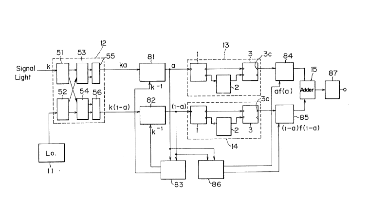
FIG. 11 is a block diagram showing a first
embodiment of the polarization diversity receiver for
coherent optical communication according to the present
invention.
The optical-electrical converter 12 is
arranged for example as described below. In the present
embodiment, the optical-electrical converter 12 is made
up of a first and a second polarization beam splitter 51
and 52, respectively separating the signal light and the
local light into polarization components of which the
~04728~
planes of polarization are orthogonal to each other, a
first and a second optical coupler 53 and 54
respectively adding up the polarization components from
the polarization beam splitters having the same plane of
polarization in one and the other direction and then
bisecting the combined light and outputting the bisected
light beams and a first and a second optical detecting
circuit 55 and 56 for optical-electrical conversion of
the light from the optical couplers into IF signals. By
the use of a fiber coupler of a polarization-plane
main~aining type, the state of polarization of the light
input to the optical detecting circuits 55 and 56 (the
specific polarization component of the signal light and
the specific polarization component of the local ligh~)
can be defined so that the detecting efficiency is
enhanced.
FIG. 12 shows an example of structure of the
optical detecting circuit 55, 56. In this e~ample, the
optical detecting circuit 55, 56 includes a single
photodetector element 61 of a PIN photodiode or the
like, and each photodetector element 61 is adapted to
receive one portion of the light beams bisected by the
first and second optical couplers 53 and 54. The
photodetector element 61 is applied with a reverse bias
26
2~47284
as usual and the optical current produced in the
photodetector element 61 is passed through a load
resistor 62. The IF signal generated as the change in
potential at the junction of the photodetector element
61 and the load resistor 62 is amplified by a front-end
amplifier 63 to be output from the optical detecting
circuit 55, 56. If it is permitted by the optical
arrangement, both portions of light beams bisected by
the optical coupler 53, 54 may be detected by a single
photodetector element 61.
Structure of a double balanced type optical
detecting circuit as another example of structure of the
optical detecting circuit 55, 56 is shown in FIG. 13.
In the structure shown in FIG. 13A, it is adapted such
that changes in the optical currents produced in two
photodetector elements 71 and 72 formed of a PIN
photodiode or the like and are of substantially the same
characteristics are extracted as voltage changes, which
are respectively amplified in front-end amplifiers 73
and 74 and then subjected to subtraction in a subtractor
75. In the described arrangement, by equalizing the
lengths of the optical paths of the light beams entering
the photodetector elements 71 and 72 from the coupler 53
or 54, the signal components input to the photodetector
2047284
elements 71 and 72 are rendered in antiphase and the
intensity noise components of the local light are
rendered in phase as the result of inversion of optical
phase in the optical coupler. Accordingly, the signal
components are added together and the intensity noise
components are canceled with each other so that the
effect of the intensity noise of the local light can be
suppressed. Further, since both portions of the light
beam bisected by the optical coupler can be economically
used, the reception sensitivity is advantageously
improved. It is also well to arrange as shown in FIG.
13B such that photodetector elements 71 and 72 similarly
of the same characteristics are connected in series and
the change in potential at the junction is output after
being amplified by a front-end amplifier 76.
In the arrangement of the optical-electrical
converter 12 shown in FIG. 11, in order to enhance the
interference efficiency between the signal light and the
local light, polarization beam splitting is applied to
both the signal light and the local light and,
thereafter, the optical detection is performed for each
of the polarization components. However, optical
detection may also be achieved by adding linearly
polarized local light obtained by means of polarization
28
~047284
maintaining fiber coupler, not by means of polarization
beam splitting, to each of polarization components of
the signal light obtained by the polarization beam
splitting. Further, in the illustrated case, the signal
light and the local light are each first subjected to
polarization beam splitting in the polarization beam
splitters and then added together and bisected by the
optical couplers, but the signal light and the local
light may be first added together and bisected by an
optical coupler and then subjected to polarization beam
splitting in a polarization beam splitter.
Referring to FIG. 11, reference numerals 81
and 82 denote a first and a second variable gain
amplifier for respectively amplifying the IF sigrlals
input from the optical-electrical converter 12 to first
and second demodulators 13 and 14, and 83 denotes a
first gain controlling circuit for detecting the power
of the IF signals for each of the polarization
components and controlling the gains of -the amplifiers
81 and 82 so that the sum total of the power may be kept
constant. By the provision of such control loop, it
becomes possible to supply the first and second
demodulators 13 and 14 with IF signals of constant total
power, not suffering from undesired power variations of
29
~017284
-
the signal light. The reason why the sum total of the
power is here controlled to be constant is because the
sum total of the power is proportional to the power of
the received signal light. More specifically, the
optical currents produced in the photodetector elements
of the photo detecting circuits 55 and 56 are each
proportional to the square root of the product of the
power of the signal light and the power of the local
light and the power of the IF signal is proportional to
the square of the optical current, and therefore, the
sum total of the power of the IF signals obtained for
each of the polarization components becomes proportional
to the power of the received signal light.
In the present embodiment, there are provided
a third and a fourth variable gain amplifiers 84 and 85
respectively amplifying the signals input from the first
and second demodulators 13 and 14 to the adder 15 and a
second gain controlling circuit 86 for detecting the
power of the IF signals for each of the polarization
components and controlling the gains of the third and
fourth variable gain amplifiers 84 and 85 on the basis
of a weighting function, in which the ra-tio of division
of the power is taken as a parameter. Reference numeral
87 denotes a discriminator.
20472~
By having the signals weighted as described
above, it can be arranged such that a demodulated signal
of smaller power is output from that demodulator which
is supplied with an IF signal of smaller power, of the
first and second demodulators 13 and 14, while a
demodulated signal of larger power is output from that
demodulator which is supplied with an IF signal of
larger power, and therefore, the increase of the noise
due to the provision of two demodulators can be
suppressed to a minimum and the reception sensitivity
can be enhanced.
In the case where digital circuit elements
such as the demodulator of the present invention are
used, there is the possibility that the demodulator
makes a malfunction when an input signal beyond the
input dynamic range is input thereto. Accordingly, in
the preferred embodiment of the present invention, a
weighting function is employed whereby an output signal
is cu-t off when an IF signal at a level beyond a
predetermined range is input. More specifically, in the
preferred embodiment of the present invention, when the
divided ratio of the power bet~een the intermediate-
frequency signals respectively input to the first and
second demodulators 13 and 14 is denoted as a~ a),
~047284
the weighting function f(a), using a cutoff point b
expressed as
b = 10- D t 10
where D (dB) represents the input dynamic range of the
first and second demodulators 13 and 14, is set up as
O (O ~ a ~ b)
f(a) = {
a (b < a ~ 1)
and the gains in the third and fourth variable gain
arnplifiers 84 and 85 are controlled to be respectively
proportional to af(a) and (1 - a)f(1 - a). A graph of
the weighting function f(a) when the dynamic range is 6
dB is shown in FIG. 14. In this case, the cutoff point b
is 0.25.
Now, the deterioration in -the reception
sensitivity in the case where the weighting function
f(a) as shown in FIG. 14 is adopted will be considered.
Generally, the quantity of deterioratiorl d
from the ideal signal-to-noise ratio is expressed as a
function of the weighting function f(a) as
[{af(a)}l/ 2 + {(l-a)f(1-a)}1/ 2 ] 2
d = 10 log1o [dB]
f(a) + f(l-a)
The relationship between the deterloration
(dB) in the reception sensitivity and a when the
weighting function f(a) as shown in FIG. 14 is adopted
32
20~7284
is shown in FIG. 15. When 0 < a ~ b, hence f(a) = 0,
the deterioration in the reception sensitivity varies
along the selective combining law, whereby selective
demodulation is performed only for a relatively large
demodulated signal, and in this case, deterioration in
the reception sensitivity varies in dependence on a. On
the other hand, when b < a ~ 1, hence f(a) = a, the
deterioration in the reception sensitivity varies along
the maximal ratio combining law. That is, in this case,
there in no deterioration in the reception sensitivity.
As apparent from FIG. 15, the deterioration in
the reception sensitivity becomes a maximum when a = b,
and therefore, decreasing b is effective for improving
the reception sensitivi-ty. That is, the deterioration
in the reception sensitivity can be suppressed by
forming the first and second demodulators with digital
circuit elements having a larger input dynamic range.
FIG. 16 is a graph showing the relationship
between the deterioration in the reception sensitivity
and the input dynamic range. It is apparent that the
deterioration in the reception sensitivity decreases as
the dynamic range increases. When the dynamic range is
over 20 dB, the deterioration in the reception
sensitivity becomes under 0.1 dB and then a practically
~04728~
satisfactory reception sensitivity can be obtained.
In the present embodiment, as described above,
it is adapted such that weighting of demodulated signals
is performed along the maximum ratio combining law as
much as possible before they are added up and the
weighting along the maximum ratio combining law is given
up depending on the input dynamic range of the
demodulator and it is shifted over to the selective
combining law.
Weighting along the maximum ratio combining
law can be achieved also by employing another weighting
function than that used in the above described example.
More specifically, in another preferred embodiment of
the present invention, when the divided ratio of the
power of the intermediate-frequency signals respectively
input to the first and second demodulators 13 and 14 is
denoted as a~ a), the weighting function f(a), using
a cutoff point b expressed as
b = 10- D / 1 0
where D (dB) represents the input dynamic range of the
first and second demodulators 13 and 14, and also using
a function
f1(a) = a/F(1/2 - a),
where F(1/2 - a) is an even function,
34
204728~
is se-t up as
0 (0 ~ a ~ b)
f(a) = {
f1(a) (b < a ~ 1)
and the gains in the third and fourth variable gain
amplifiers 84 and ~5 are controlled to be respectively
proportional to af(a) and (1 - a)f(1 - a). It is
apparent that the same effect as obtained in the
preceding embodiment can be obtained in this case in
view of the structure of the weighting function.
In executing the weighting, it is preferred
that the cutoff point _ is set to b < 0.5. In other
words, it is preferred that the input dynamic range of
the demodulator is set larger than 3 dB. This is
because, unless the cutoff point b or the input dynamic
range D satisfies the above described condition, the
portion being along the maximum ratio combining law in
FIG. 15 gets substantially lost and it becomes unable to
effectively remedy the deteriorating reception
sensitivity.
FIG. 17 is a block diagram showing a second
embodiment of the polarization di~ersity recei~-er for
coherent optical communication according to the present
invention. What is different in this embodiment from
the first embodiment is that the structure of the second
2~4728~
embodiment includes, in addition to the structure of the
first embodiment, an automatic frequency control circuit
(AFC circuit) 91 for detecting the frequency of the IF
signal and controlling the frequency of the local ligh1
so -that the frequency of the IF signal may be held
constant. The IF signal to be input to the AFC circuit
91 may be obtained from the output port of the first and
second variable gain amplifiers 81 and 82 as shown in
the diagram or it may be obtained from the output port,
not shown, of the optical-electrical converter 12. With
this arrangement, it becomes possible to obtain an IF
signal whose center frequency is held constant
regardless of any undesired frequency variation
occurring in the signal light and/or the local light
and, therefore, a normal demodulation operation can be
secured.
FIG. 18 is a block diagram showing a third
embodiment of the polarization diversity receiver for
coherent optical communication according to the present
invention. What are different in this embodiment from
the second embodiment are that it employs the
demodulators of the third basic structure instead of the
demodulators of the first basic structure and includes,
instead of the AFC circuit 91, an AFC circuit 101
36
~047284
detecting the average level of the demodulated signals
for controlling the frequency of the local light such
that the average level is held constant. The
arrangement using a subtractor for combining the
demodulated signals as shown in the third basic
structure is easier to realize than that using arl adder
for combining the demodulated signals, especially when
the bit rate of the demodulated signal is high, because
a subtractor of a very simple structure can be realized
through the use of a differential pair of transistors
when the circuits are arranged in an IC. The reason why
the average level (DC level) of the demodulated signals
is detected in the AFC circuit 101 is because the
demodulators 13 and 14 function also as a frequency
discriminator and the average level of the demodulated
signals depends on the frequency of the IF signal.
Accordingly, the use of such AFC circuit 101 eli~llinates
the need for a frequency-voltage converter in the AFC
circuit and simplifies -the structure of the AFC loop.
Incidentally, the AFC control is also applicable to the
case where the demodulator of the first basic structure
is employed.
According to the present invention, as
described above, an effect can be obtained that the
37
204728~
structure can be simplified of the polarization
diversity receiver for coherent optical communication
for coping with the variation in the polarization state
of the signal light at the receiving end. Further,
since the demodulator is formed of digital circuit
elements, such effects can be obtained that the
electronic circuit portion of the receiver can be
arranged into an IC and the apparatus can be made
smaller in size and that mass production of the
apparatus can be made easier. Besides, by weighting the
demodulated signals in accordance with a specific
weighting function, such an effect can be obtained that
a malfunction of the demodulator is prevented.
In the foregoing, the present invention is
described as related to specific embodiments but the
present invention is not limited to details of such
embodiments. For example, embodiments can be made on
the basis of the second or the fourth basic structure of
the polarization diversity receiver for coherent optical
communication similarly to the embodiment on the basis
of the first or the third basic structure. Further, as
the OR/NOR circuit of the demodulator in the present
invention, the portion of the circuit elements of the
exclusive OR/NOR circuit functioning as the OR/NOR
38
~0~728~
circuit can be used.
Thus, preferred embodiments described herein
are given by way of illustration only and not limitative
of the present invention. The scope of the invention is
defined by the appended claims and all changes and
modifications as fall within the equivalence of the
scope of the claims are therefore to be embraced by the
invention.
39