Note: Descriptions are shown in the official language in which they were submitted.
20~7308
The present invention generally relates to a radio
communication apparatus which receives a digital modula-
tion signal. More particularly, this invention pertains
to an apparatus and a method for demodulating a received
digital modulation signal.
GMSK (Gaussian filtered Minimum Shift Keying),
which is known as one of narrow-band digital modulation
systems, is used in mobile communications involving a
mobile radiophone or a portable radiophone, for example.
This radio communication apparatus for mobile com-
munications performs frequency detection to demodulate a
received GMSK modulation signal to a digital signal of a
base band, periodically samples the voltage level of the
detection signal, and identifies data according to each
sampled level. In identifying data, the sampled level
is compared with two threshold voltages Ll and L2 for
data discrimination. When the sampled level is higher
than the voltage Ll, the data is discriminated to be "1"
while when the former is lower than the voltage L2, the
data is judged to be "0".
The above-described radio communication apparatus
is generally equipped with a digital PLL circuit to
reproduce a clock necessary to sample the detection
signal. In this case, this apparatus detects a zero
cross where the frequency detection signal crosses the
zero level in accordance with a change in data, and
generates a zero-cross signal to trigger the PLL circuit
2047308
-- 2
at each zero cross point. When the zero-cross signal
triggers the PLL circuit, the PLL circuit controls the
phase of the zero-cross signal which is generated in
accordance with the data rate frequency in the radio
communication apparatus, and reproduces a clock
synchronous with the detection signal.
When the frequency detection signal is distorted or
noise is increased due to deterioration of the receiving
conditions, zero crossing frequently occurs in other
points than actual data-altering points. If the PLL
circuit is triggered in association with every zero
cross, the clock used for sampling the detection signal
will not correctly be reproduced.
Published Unexamined Japanese Patent Application No.
Hei 1-240024 published September 25, 1989 discloses the
art for preparing a predicting time slot signal to
predict the next zero-cross point based on the reproduced
clock, and controlling the phase of the reproduced clock
at the zero-cross point only when a zero cross occurs
within the time slot.
Fig. 1 illustrates a clock reproducing circuit
disclosed in this prior art. A GMSK modulation signal
is received by an antenna 1, and is in turn detected
by a frequency detector 2. A detection signal, the
output from the detector 2, is supplied to a zero-cross
selector 3. The zero-cross selector 3 includes a
comparator 11, an exclusive OR (EX-OR) gate 12, an AND
gate 13, a D type flip-flop 14, an RS flip-flop 15 and
2047308
an inverter 16, as shown in Fig. 2. The zero-cross
selector 3 detects each zero cross of the detection
signal, and generates a zero-cross signal corresponding
only to the zero cross, which has been detected while a
time slot signal is supplied from a time slot signal
generator 4. Based on a reproduced clock signal to be
described later, the time slot signal generator 4 pre-
dicts the zero cross of the next detection signal, and
generates the time slot signal during a predetermined
period of time including a timing to be predicted as
shown in Fig. 3. A high stable fixed oscillator 9
generates a pulse at a frequency N times as high as the
data rate frequency of a digital signal, and supplies
the pulse as a clock signal to a phase controller 8.
The phase controller 8 controls the phase of the clock
signal, and sends that signal to a frequency divider 5.
The frequency divider 5 frequency-divides the clock
signal into the data rate frequency, and generates a
reproduced clock signal. A phase comparator 6 compares
the phase of the zero-cross signal from the zero-cross
selector 3 with that of the reproduced clock signal from
the frequency divider 5, and supplies a phase difference
signal corresponding to the resultant phase difference
to a sequential filter 7. Based on the phase difference
signal, the sequential filter 7 supplies a lead signal
to the phase controller 8 when the reproduced clock
signal lags behind the zero-cross signal, while sending
2047308
- 4 -
a lag signal to the controller 8 when the reproduced clock
signal leads the zero-cross signal. In response to the lag
signal, the phase controller 8 eliminates part of a train
of the pulses included in the clock signal to be sent from
the high stable fixed oscillator 9. When receiving the
lead signal, the phase controller 8 adds a pulse to the
pulse train included in the clock signal. The phase of the
reproduced clock signal lags when the frequency divider 5
frequency-divides the clock signal with part of the pulse
train eliminated, while it leads when the divider 5
frequency-divides the clock signal with some pulse added to
the pulse train. The reproduced clock signal is always
controlled as described above, to be synchronized with the
detection signal.
Published Unexamined Japanese Utility Model
Application No. Hei 2-8243 published January 19, 1990
discloses the art of compensating for the center level of a
detection signal before identifying data. Fig. 4
illustrates a level compensator disclosed in this document.
The compensator comprises an antenna 21, a frequency
detector 22, a subtractor 23, a data discriminating circuit
24 and a level detector 25. A GMSK modulation signal,
received at the antenna 21, is detected by the detector 22.
The detector 22 generates a detection signal to be supplied
through the subtractor 23 to the data discriminating
circuit 24 and the level detector 25. This detection
2047308
signal is represented in the form of an eye pattern in
Fig. 5. "VR" represents a reference voltage, "Vl" and
"V2" are first and second decision levels, "vs" is a
signal amplitude, and "V(i-2)", "V(i-1)", "V(i)",
"V(i+l)" and "V(i+2)" are signal voltage levels
corresponding to a series of data. The level detector
25 includes an A/D converter 26, a clock reproducing
circuit 27, an error signal generator 28, an integrator
29 and a D/A converter 30. The A/D converter 26 shifts
the voltage level of the detection signal by the
reference voltage VR and performs A/D conversion on the
sifted level of the detection signal, which is in turn
supplied to the error signal generator 28. The error
signal generator 28 compares the level of the voltage
undergone the A/D conversion, for example, V(i), with
those of the threshold voltages Vl and v2 for phase
detection. The error signal generator 28 determines the
following augmenters: V(i) - Vs when V(i) > Vl, V(i)
when v2 < V(i) < Vl, and V(i) + Vs when v(i) < v2. The
individual augmenter corresponds to the drift from the
center frequency level of the detection signal. The
error signal generator 28 generates a signal of the
reference voltage VR subtracted from the augmenter, as
an error signal. The integrator 29 integrates the error
signal, on which the D/A converter 30 then performs D/A
conversion. The subtractor 23 subtracts the output
signal from the D/A converter from the detection signal,
2047308
-- 6
to set the center level of the detection signal exactly
to "zero." The data discriminating circuit 24 discrimi-
nates data based on the detection signal acquired in
this manner.
The clock reproducing circuit shown in Fig. 1,
however, malfunctions when noise is superposed on the
detection signal within a predicted period of time that
a time slot signal indicates. Should noise a be
superposed on the detection signal as shown in Fig. 6,
the timing at which the output of the AND gate 13 should
rise would be shifted to time t' from the normal rising
time t.
Further, when the frequency of a GMSK modulation
signal is detected, distortion of a wave causes the
detection signal not to zero-cross at a data-altering
time as shown in Fig. 7. Points A, B, B', C and D in
Fig. 3 corresponds to points A, B, B', C and D of the
detection signal in Fig. 7. If data is altered at time
tB, the detection signal normally zero crosses at point
s. In the case that distortion of a waveform makes
detection signal zero-cross at point B, the output of
the AND gate 13 rises at time ts', instead of tB as
shown in Fig. 3.
The detection signal zero-crosses at point D where
time tD corresponds to a point where data is altered.
If the detection signal includes the point B', where the
zero cross is made by the different timing from when
2047308
data is altered, and the point D, where the zero cross
occurs at the timing corresponding to when data is
changed, the phase of a reproduced clock signal fluc-
tuates, i.e., a so-called jitter occurs. This bothers
stable reception of the signal.
The level compensator shown in Fig. 4 refers to a
timing at which the detection signal crosses the
reference level VR in order to control the phase of the
reproduced clock signal. When the center level of the
detection signal coincides with the reference voltage VR
as illustrated in Fig. 5, even if the phase of a repro-
duced clock is shifted, the level compensator acquires a
phase difference ~ between time ti when the detection
signal crosses the reference voltage VR and time tj when
the reproduced clock is changed, and controls the phase
of the reproduced clock.
In the case that the detection signal somehow has
its center frequency level shifted from the reference
voltage VR, the following shortcoming would occur. If
the center level of the detection signal is shifted up,
points, such as B1 and D, are where the detection signal
crosses the reference voltage VR. Even if the repro-
duced clock is properly synchronized with the detection
signal, the phase of the reproduced clock does not
coincide with the detected cross points D and Bl. The
phase of the reproduced clock leads when the cross at
the point D is detected, while it lags when the cross at
2047308
-- 8 --
the point Bl is detected. As a result, the reproduced
clock will not be synchronized with the detection
signal.
Further, if the phase of the reproduced clock is
shifted with respect to the detection signal, the repro-
duced clock cannot be synchronized with the detection
signal. When the cross of the signal is detected at the
point B, a phase difference 0 between this cross and the
reproduced clock is zero, thus requiring no phase
control of the reproduced clock. When the signal
crossing at the point D is detected, the phase of the
reproduced clock will be erroneously adjusted based on a
phase difference ~' between this cross and the repro-
duced clock.
There is another shortcoming in the case of compen-
sating for the center level of the detection signal.
The error signal generator 28 determines V(i) - vs as an
augmenter when V(i) > Vl. When the GMSK modulation
signal is subjected to frequency detection, the
resultant detection signal has a level V(i) > Vl at
three points Al, A2 and A3. More specifically, augmen-
ters at these points should be v(l) - Vsl, V(i) - vs2
and V(i) - vs, respectively. If all the augmenters are
determined as V(i) - vs, however, a compensation
difference will occur at the points Al and A2. The
same is true of when V(i) < v2.
The occurrence of the compensation difference
2047308
described above supposes no phase shift in the repro-
duced clock signal. If the reproduced clock signal has
its phase shifted, A/D conversion will be performed on
the level at the point B3, instead of the level at the
point Al. The exact augmenter in this case is V(i) -
vs3. When the augmenter is determined as V(i) - vs or
V(i) - Vsl, the phase shift in the reproduced clock
signal causes erroneous compensation for the center
level of the detection signal, although that level is
not actually shifted.
It is therefore an object of the present invention
to provide a demodulating apparatus and a demodulating
method, which are hardly affected by noise or a phase
jitter in phase control of a reproduced clock.
To achieve this object, according to one aspect of
the present invention, there is provided a demodulating
apparatus comprising: a frequency detector for per-
forming a frequency-detection on a digital modulation
signal to acquire a detection signal; a clock generator
for generating a clock signal; and a discrimination sec-
tion for sampling a voltage level of the detection
signal from the frequency detector at a clock timing of
the clock signal from the clock generator, and
converting the sampled voltage level into digital data,
which is set to have one of first and second logic
values on the basis of a reference voltage LDC; wherein
the discrimination section includes a control circuit
- lO 2047308
for comparing the voltage level En sampled at a clock
timing, voltage level En-l sampled at a timing one clock
earlier than En and voltage level En-2 sampled at a
timing two clock earlier than En, with first and second
threshold voltages LA and LB respectively higher and
lower than the reference voltage LDC, and controlling
the clock generator to synchronize the phase of the
clock signal with the detection signal when it is
detected from the comparison that anyone of first and
second conditions is satisfied where the first condition
is En-2 < LB, LB < En-l < LA and LA < En, and the second
condition is LA < En-2, LB < En-l ~ LA and En < Ls.
According to another aspect of the present inven-
tion, there is provided a demodulating method compris-
ing: a first step of performing a frequency-detection on
a digital modulation signal to acquire a detection
signal; a second step of generating a clock signal; a
third step of sampling a voltage level of the detection
signal at a clock timing of the clock signal, and con-
verting the sampled voltage level into digital data,which is set to have one of first and second logic
values on the basis of a reference voltage LDC; and a
fourth step of comparing the voltage level En sampled at
a clock timing, voltage level En-l sampled at a timing
one clock earlier than En and voltage level En-2 sampled
at a timing two clock earlier than En, with first and
second threshold voltages LA and LB respectively higher
11 2047~08
and lower than the reference voltage LDC, and control-
ling the phase of the clock signal to be synchronized
with the detection signal when it is detected from the
comparison that anyone of first and second conditions is
satisfied where the first condition is En-2 < LB, LB <-
En-1 S LA and LA < En, and the second condition is LA <
En-2, LB < En-1 < LA and En < LB.
According to the demodulating apparatus and demodu-
lating method of the present invention, the phase dif-
ference between a reproduced clock and a detection
signal is detected under more appropriate conditions, so
that the phase of the reproduced clock will not easily
be affected by noise and a phase jitter.
This invention can be more fully understood from
the following detailed description when taken in con-
junction with the accompanying drawings, in which:
Fig. l is a diagram illustrating the arrangement of
a conventional clock reproducing circuit;
Fig. 2 is a diagram illustrating the arrangement of
a zero-cross selector shown in Fig. l;
Fig. 3 is a waveform diagram of signals to be pro-
cessed by the zero-cross selector shown in Fig. 2;
Fig. 4 is a block diagram illustrating the arrange-
ment of a conventional level compensator;
Fig. 5 is a waveform diagram of detection signals
and reproduced clock signals which are processed by the
level compensator in Fig. 4;
- 12 - 2047308
Fig. 6 is a waveform diagram for explaining when
noise is superposed on the detection signal shown in
Fig. 2;
Fig. 7 is a waveform diagram for explaining a shift
of the zero cross of the detection signal;
Fig. 8 is a waveform diagram for explaining a shift
of the center level of the detection signal;
Fig. 9 is a block diagram illustrating the demodu-
lation section of a radio communication apparatus
according to the first embodiment of the present inven-
tion;
Fig. 10 is a flowchart showing the operation of the
microcomputer shown in Fig. 9;
Figs. 11 and 12 are waveform diagrams for
explaining the phase control on the clock signal;
Fig. 13 is a flowchart showing the operation of a
microcomputer used in a radio communication apparatus
according to the second embodiment;
Figs. 14 to 16 are flowcharts showing the operation
of a microcomputer used in a radio communication appara-
tus according to the third embodiment; and
Figs. 17 through 21 are waveform diagrams for
explaining the phase control on the clock signal in the
third embodiment.
A radio communication apparatus according to the
first embodiment of the present invention will now be
described referring to Figs. 9 through 12.
- 13 - 2047308
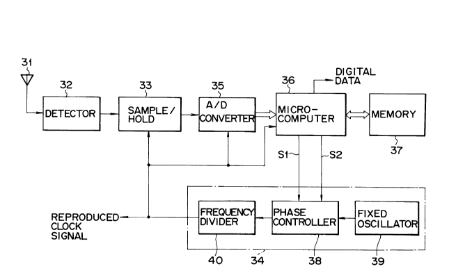
Fig. 9 illustrates the circuit structure of the
demodulation section in the radio communication appara-
tus. This demodulation section includes a frequency
detector 32, a sample and hold (sample/hold) circuit 33,
5 a clock signal generator 34, an A/D converter 35, a
microcomputer 36 and a memory 37. A GMSK modulation
signal is received by an antenna 31 and is in turn
supplied to the detector 32. The detector 32 performs a
frequency-detection on the modulation signal, and
supplies a resultant detection signal to the sample/hold
circuit 33. The sample/hold circuit 33 performs
sampling on the voltage level of the detection signal by
the clock timing of a reproduced clock signal to be sent
from the clock signal generator 34, and supplies the
sampled voltage to the A/D converter 35. The A/D con-
verter 35 then converts the voltage level obtained by
sampling into level data, which is sent to the microcom-
puter 36. The microcomputer 36 stores the level data
from the A/D converter 35 in the memory 37, and uses
20 this level data and previously stored level data to
control the phase of the reproduced clock signal. A
reference voltage LDC, and the first to fourth threshold
voltages Ll, L2, LA and LB, which are determined
according to the characteristics of circuits, such as
25 the detector 32 and the A/D converter 35, are stored as
preset data in the memory 37. The preset data may be
prepared by the microcomputer 36 and be stored in the
- 14 - 2047308
memory 37. In this case, GMSK modulation is performed
on a dummy digital signal in advance. When receiving
the GMSK modulation signal corresponding to the dummy
digital signal, the microcomputer 36 prepares the preset
data based on the level data to be sent from the A/D
converter 35. The reference voltage LDC is used to
shift the voltage level of the detection signal, and the
center level of the detection signal is set to the
reference voltage LDC at the starting of communication.
The first and second threshold voltages Ll and L2 are
used for determining whether the sampled level of the
detection signal is "1" or "O." The third and fourth
threshold voltages LA and LB are used for the phase
detection of the clock signal. The threshold voltage Ll
and LA are higher than the reference voltage LDC, and
the threshold voltages L2 and LB are lower than
reference voltage LDC. The clock signal generator 34
comprises a fixed oscillator 39, a phase controller 38
and a frequency divider 40. The fixed oscillator 39
oscillates a clock pulse by the frequency N times as
much as data rate frequency of the digital signal, and
sends this pulse as a clock signal to the phase
controller 38. The phase controller 38 then controls
the phase of the clock signal and supplies it to the
frequency divider 40. The frequency divider 40 divides
the clock signal by N to generate a reproduced clock
signal with the data rate frequency. This reproduced
- 15 - 2047308
clock signal is supplied as a timing signal to the
sample/hold circuit 33, the AiD converter 35 and the
microcomputer 36.
The microcomputer 36 is programmed to perform pro-
cessing as illustrated in Fig. 10 in a demodulation
operation. The microcomputer 36 checks in step STl
whether or not the level data En from the A/D converter
35 is received. When the reception of the level data En
is confirmed, the microcomputer 36 stores En into the
memory 37, and compares level data, En, En-l and En-2,
the latter two having been stored in the memory 37
before the level data En, with the third threshold
voltage LA and the fourth threshold voltage LB in step
ST2. In subsequent step ST3, it is checked if the first
condition of En-2 < LB, LB ~ En-l < LA and LA < En is
satisfied. If the first condition is not satisfied, it
is checked in step ST4 if the second condition of LA <
En-2, LB S En-l < LA and En < LB iS satisfied. If the
second condition is not satisfied either, the microcom-
puter 36 sets the level data En-l stored in the memory
37 to the level data En-2, and sets the level data En to
the level data En-l in step ST5. Then, the microcom-
puter 36 returns to step STl.
If the first condition of En-2 < LB, LB < En-l < LA
and LA < En is satisfied in step ST3, it is then checked
if En-l < LDC in step ST6. If En-l < LDC, the microcom-
puter 36 generates a lag signal S2 and sends it to the
- 16 - 2047308
phase controller 38 in step ST7 before executing step
ST5. If En-l < LDC is not detected in step ST6, it is
then checked if En-l > LCD in step ST8. If En-l > LDC,
the microcomputer 36 generates a lead signal Sl and
sends it to the phase controller 38 in step ST9 before
executing step ST5. If En-l = LDC is detected in step
ST8, step ST5 will be executed.
If the second condition of LA < En-2, LB S En-l 5
LA and En < LB is satisfied in step ST4, it is then
checked if En-l < LDC in step ST10. If En-l < LDC, the
microcomputer 36 generates the lead signal Sl and sends
it to the phase controller 38 in step STll before exe-
cuting step ST5. If En-l < LDC is not detected in step
ST10, it is then checked if En-l > LCD in step ST12. If
En-l > LDC, the microcomputer 36 generates the lag
signal S2 and sends it to the phase controller 38 in
step ST13 before executing step ST5. If En-l = LDC is
detected in step ST12, step ST5 will be executed.
The phase controller 38 receives the clock signal
from the fixed oscillator 39, removes part of a pulse
train included in this clock signal in response to the
lag signal S2, and adds a pulse to the pulse train
included in the clock signal in response to the lead
signal Sl. The phase of the reproduced clock signal
lags when the frequency divider 40 frequency-divides the
clock signal with part of the pulse train removed, and
it leads when the frequency divider 40 frequency-divides
- 17 - 2047308
the clock signal having a pulse added to this pulse
train. In this manner, the reproduced clock signal is
always controlled to be synchronized with the detection
signal.
According to the first embodiment, when fetching
the level data En of the detection signal from the A/D
converter 35, the microcomputer 36 checks if the first
condition of En-2 < LB, LB < En-1 < LA and LA < En is
satisfied. If the first condition is not satisfied, the
microcomputer 36 checks if the second condition of
LA < En-2, LB < En-l < LA and En < LB iS satisfied.
When the first condition is satisfied, it is then
checked if the level data En-l is lower than the
reference voltage LDC. If En-l < LDC, it is determined
that the phase of the reproduced clock signal leads the
phase of the detection signal, and the lag signal S2 is
supplied to the phase controller 38. If En-l > LDC, it
is determined that the phase of the reproduced clock
signal lags behind the phase of the detection signal,
and the lead signal Sl is supplied to the phase
controller 38. If En-l = LDC, it is determined that the
phase of the reproduced clock signal is normal, and
neither the lag signal nor the lead signal is supplied
to the phase controller 38.
When the second condition is satisfied, it is then
checked if the level data En-1 is lower than the
reference voltage LDC. If En-l < LDC, it is determined
2047308
that the phase of the reproduced clock signal lags
behind the phase of the detection signal, and the lead
signal Sl is supplied to the phase controller 38. If
En-l ~ LDC, it is determined that the phase of the
reproduced clock signal leads the phase of the detection
signal, and the lag signal S2 is supplied to the phase
controller 38. If En-l = LDC, it is determined that the
phase of the reproduced clock signal is normal, and
neither the lag signal nor the lead signal is supplied
to the phase controller 38.
In other words, only when the detection signal
satisfies the first condition or the second condition,
the phase of the reproduced clock is checked, and phase
control is performed when there is a phase difference.
This method can improve the stability of the phase
control, which may be deteriorated by noise and a phase
jitter, as compared with the conventional method that
compares every zero cross with the phase of the repro-
duced clock signal, so that the reproduced clock can
accurately be synchronized with the detection signal.
The phase control will be further described below
referring to Fig. ll.
In Fig. ll, point ER corresponds to the voltage
level of the detection signal at timing tR where data is
changed. If the phase of the reproduced clock is
controlled to coincides with the timing tR where data is
changed, sampling is executed in synchronism with the
2047308
-- 19 --
detection signal. Suppose that level data En, En-l and
En-2 are acquired at clock timings tn, tn-1 and tn-2,
respectively. When these data are compared with the
third threshold voltage LA and the fourth threshold
voltage LB, the first condition of En-2 < LB, LB S
En-1 S LA and LA < En is satisfied. AS the level data
En-1 is compared with the reference voltage LDC, En-l >
LDC is detected and the clock signal generator 34 is
controlled to lead the phase of the reproduced clock
signal, causing the clock timing tn-l to approach the
timing tR where data is changed.
In Fig. 12, point El-1 corresponds to the voltage
level of the detection signal at timing tl-1 where data
is changed. Suppose that level data El, El-1 and El-2
are acquired at clock timings tl, tl-1 and tl-2, respec-
tively. When these data are compared with the threshold
voltage LA and the threshold voltage LB, the first con-
dition of El-2 < LB, LB < E'-1 S LA and LA < El is
satisfied. AS the level data El-1 is compared with the
reference voltage LDC, El-l > LDC is detected. In this
case, the clock signal generator 34 is controlled to
keep the phase of the reproduced clock signal.
Suppose that level data El', El-l' and El-2' are
acquired at clock timings tl, tl-l and tl-2, respec-
tively. When these data are compared with the thresholdvoltage LA and the threshold voltage LB, the second con-
dition of El-2' < LA, LB < E'-1 < LA and LB < El' is
2047308
- 20 -
satisfied. As the level data El-l' is compared with the
reference voltage LDC, El-l' > LDC is detected. In this
case, the clock signal generator 34 is controlled to
keep the phase of the reproduced clock signal.
That is, according to this embodiment, every zero
cross is not compared with the phase of the clock
signal, but the phase shift of the clock signal is
checked only when the first condition or second con-
dition is satisfied, and phase control is executed to
compensate for the phase shift.
The detection signal that satisfies the first con-
dition has a waveform passing all of three points Em-l,
El-l and Em in Fig. 12. The detection signal that
satisfies the second condition has a waveform passing
all of three points Em-l', El-l and Em' in Fig. 12.
Only when there appears a waveform which satisfies
one of the first and second conditions, therefore,
sampling is performed at a clock timing tn-l between
clock timings tm-l and tm, and phase control is executed
so that the level data En-l acquired by the sampling
coincides with the reference voltage LDC or En-l becomes
El-l, thereby permitting the phase of the clock signal
to be synchronized with that of the detection signal.
According to this embodiment, therefore, the phase
control is not executed when the detected waveform
passes points A, B', B and C (Em'), although it crosses
the reference voltage LDC with an error, as shown in
2047308
- 21 -
Fig. 12.
According to the above-described embodiment, the
microcomputer 36 generates a pulse signal as the lead
signal Sl and lag signal S2. When first or second con-
dition is satisfied, the microcomputer 36 supplies one
pulse as the lead signal Sl or lag signal S2 to the
phase controller 38. Upon reception of one pulse as the
lead signal Sl, the phase controller 38 performs the
phase control to lead the phase of the reproduced clock
by l/N period. Upon reception of one pulse as the lag
signal S2, the phase controller 38 performs the phase
control to lag the phase of the reproduced clock by l/N
period. This control relatively takes time until the
phase of the clock is synchronized with that of the
detection signal after occurrence of a phase shift, but
can reduce a phase difference originated from noise on
the detection signal.
With regard to the phase control, the above embodi-
ment may be modified as follows.
According to the first modification, the lead
signal Sl and lag signal S2 indicates not only the phase
leading and phase lagging of the reproduced clock, but
also the phase difference between the reproduced clock
and the detection signal. The microcomputer 36 detects
the difference between the voltage level En-l of the
detection signal sampled at tn-l and the reference
voltage LDC, determines the phase augmenter based on
20~7308
- 22 -
this difference, and supplies the lead signal Sl or lag
signal S2 of the level corresponding to this phase
augmenter to the phase controller 38. The phase
controller 38 performs such phase control as to lead the
phase of the reproduced clock by an M/N period upon
reception of the lead signal S1, and as to lag the phase
of the reproduced clock by an M/N period upon reception
of the lag signal S2, where M is a positive integer that
varies in accordance with the level of the lead signal
0 Sl or lag signal S2, and is proportional to the phase
augmenter. The phase augmenter is set large when the
reproduced clock is considerably shifted from the detec-
tion signal, while it is set small when there is a small
shift between the reproduced clock and detection signal.
Although this phase control may provide an inaccurate
phase augmenter when noise is put on the detection
signal, it can shorten the time required to provide
synchronization between the reproduced clock and the
detection signal.
According to the second modification, the microcom-
puter 36 exceptionally generates the lead signal Sl and
lag signal S2 in the manner done in the first modifica-
tion only immediately after data reception has started.
More specifically, the phase augmenter of the reproduced
clock is set to an M/N period per step when data recep-
tion starts, and is fixed to a l/N period per step
thereafter. This phase control permits the phase of the
- 23 - 2047308
reproduced clock to be synchronized with the detection
signal quickly after the data reception has started,
thereby suppressing a phase difference originated from
noise superposed on the detection signal after the
synchronization has been established to accurately main-
tain the synchronization.
A radio communication apparatus according to the
second embodiment of the present invention will be
described below referring to Fig. 13. The demodulation
section of this radio communication apparatus is the
same as the one used in the first embodiment except the
structure of the microcomputer 36. The following will
describe where the second embodiment differs from the
first embodiment.
The microcomputer 36 of the second embodiment is
programmed to perform the processing as illustrated in
Fig. 13. The microcomputer 36 checks in step ST21
whether or not the level data En from the A/D converter
35 is received. When the reception of the level data En
is confirmed, in step ST22 the microcomputer 36 stores
En into the memory 37, and compares level data En, En-l
and En-2, the latter two having been stored in the
memory 37 before the level data En, with the third
threshold voltage LA and the fourth threshold voltage
LB. In subsequent step ST23, it is checked if the first
condition of En-2 < LB, LB < En-l < LA and LA < En is
satisfied. If the first condition is not satisfied, it
- 24 - 2047308
is checked in step ST24 if the second condition of LA <
En-2, LB < En-l < LA and En < LB iS satisfied. If the
second condition is not satisfied either, the microcom-
puter 36 sets the level data En-l stored in the memory
37 to the level data En-2, and sets the level data En to
the level data En-l in step ST25. Then, the microcom-
puter 36 returns to step ST21.
When the first condition is satisfied in step ST23,the level data En-l is stored as level data Vx in the
memory 37 in step ST26. In step ST27, the level data
vx~ and the level data Vx-1 and Vx-2 both previously
stored in the memory 37 are averaged, and the average
value is stored as average level data Ex in the memory
37. It is checked in step ST28 whether this average
level data Ex is lower than the reference voltage LDC.
When Ex < LDC is detected, the microprocessor 36 genera-
tes the lag signal S2 in step ST29, which is supplied to
the phase controller 38. In step ST32, the level data
Vx-l and vx which are stored in the memory 37 are set to
the level data vx-2 and Vx-l, respectively. The step
ST25 is then executed. When EX < LDC is not detected in
step ST28, it is determined in stëp ST30 if the average
level data Ex is greater than the reference voltage LDC.
When Ex > LDC is detected, the microprocessor 36 genera-
tes the lead signal Sl in step ST31 which is in turnsupplied to the phase controller 38. The level data
Vx-l and Vx stored in the memory 37 are set to the level
- 25 - 2 Oq 73 0 8
data Vx-2 and Vx-l, respectively. The step ST25 is then
executed.
When the second condition is satisfied in step
ST24, the level data En-l is stored as level data Vy in
the memory 37 in step ST32. In step ST33, the level
data Vy, and the level data Vy-l and Vy-2 both pre-
viously stored in the memory 37 are averaged, and the
average value is stored as average level data Ey in the
memory 37. It is checked in step ST34 whether this
average level data Ey is lower than the reference
voltage LDC. When Ey < LDC iS detected, the micropro-
cessor 36 generates the lead signal Sl in step ST35,
which is supplied to the phase controller 38. In step
ST38, the level data Vy-l and vy which are stored in the
memory 37 are set to the level data Vy-2 and Vy-l,
respectively. The step ST25 is then executed. When Ey
< LDC is not detected in step ST34, it is determined in
step ST36 if the average level data Ey is greater than
the reference voltage LDC. When Ey > LDC is detected,
the microprocessor 36 generates the lag signal S2 in
step ST37 which is in turn supplied to the phase
controller 38. The level data Vy-l and vy stored in the
memory 37 are set to the level data Vy-2 and Vy-1,
respectively. The step ST25 is then executed.
In the second embodiment as in the first embodi-
ment, when fetching the level data En of the detection
signal from the A/D converter 35, the microcomputer 36
- 26 - 2047308
checks if the first condition of En-2 < LB, LB S En-l <
LA and LA ~ En is satisfied. If the first condition is
not satisfied, the microcomputer 36 checks if the second
condition of LA < En-2, LB < En-l < LA and En < LB is
satisfied.
When the first condition is satisfied, the level
data En-l is stored as the level data vx in the memory
37, not being compared with the reference voltage LDC.
This level data vx and the level data Vx-l and Vx-2 both
previously stored in the memory 37 are averaged, and the
average value or average level data Ex is compared with
the reference voltage LDC. If Ex < LDC, the phase of
the reproduced clock signal is judged as leading, and
the lag signal S2 is supplied to the phase controller
38. If Ex > LDC, the phase of the reproduced clock
signal is judged as lagging, and the lead signal Sl is
sent to the phase controller 38. Further if Ex = LDC,
the phase of the reproduced clock signal is judged as
normal, and neither lead signal nor lag signal is sent
to the phase controller 38.
When the second condition is satisfied, the level
data En-l is stored as the level data vy in the memory
37, not being compared with the reference voltage LDC.
This level data vy and the level data Vy-l and vy-2 both
previously stored in the memory 37 are averaged, and the
average value or average level data Ey is compared with
the reference voltage LDC. If Ey-l < LDC, the phase of
- 27 - 2047308
the reproduced clock signal is judged as lagging, and
the lead signal Sl is supplied to the phase controller
38. If En-l > LDC, the phase of the reproduced clock
signal is judged as leading, and the lag signal S2 is
sent to the phase controller 38. Further if Ey = LDC,
the phase of the reproduced clock signal is judged as
normal, and neither lead signal nor lag signal is sent
to the phase controller 38.
In other words, only when the detection signal
satisfies the first condition or the second condition,
the phase of the reproduced clock is checked, and phase
control is performed when there is a phase difference.
This method can improve the stability of the phase
control, which may be deteriorated by noise and a phase
jitter, as compared with the conventional method that
compares every zero cross with the phase of the repro-
duced clock signal, so that the reproduced clock can
accurately be synchronized with the detection signal.
Particularly, since three level data, vx, Vx-l and
vx-2, or Vy, Vy-l and Vy-2, acquired by repetitive
sampling, are averaged in the second embodiment,
influence of noise, if present on the detection signal,
can be sufficiently decreased.
A radio communication apparatus according to the
third embodiment of the present invention will now be
described referring to Figs. 14 to 21.
The demodulation section of the radio communication
- 28 - 2047308
apparatus has the same arrangement as that of the first
embodiment, except for the arrangement in the microcom-
puter 36. The differences between this embodiment and
the first embodiment will now be explained.
The microcomputer 36 in the third embodiment is
programmed to execute processes shown in Figs. 14
through 16. AS shown in Fig. 14, the microcomputer 36
checks in step ST51 whether or not the level data En
from the A/D converter 35 is received. When the
reception of the level data En is confirmed, the
microcomputer 36 stores En into the memory 37, and com-
pares the level data En-l and En-2, which have been
stored in the memory 37 before the level data En, with
the third threshold voltage LA and the fourth threshold
voltage LB in step ST52. In subsequent step ST53, it is
checked if the first condition of En-2 < LB, LB < En-l <
LA and LA < En is satisfied. If the first condition is
not satisfied, it is checked in step ST54 if the second
condition of LA < En-2, LB < En-l < LA and En < LB is
satisfied. If the second condition is not satisfied
either, the microcomputer 36 sets the level data En-l
stored in the memory 37 to the level data En-2, and sets
the level data En to the level data En-l in step ST55.
Then, the microcomputer 36 returns to step ST51. If the
first condition is satisfied in step ST53, the microcom-
puter 36 executes the first condition process in step
ST56, and then executes step ST55. If the second
- 29 - 2047308
condition is satisfied in step ST54, the microcomputer
36 performs the second condition process in step ST57,
and then executes step ST55.
Fig. 15 illustrates the first condition process to
be performed in step ST56. When the first condition
process starts, the level data En-l is stored as level
data Eln-1 in the memory 37 in step ST60. It is checked
in step ST61 if Eln-1 < LDC. If Eln-l < LDC is
detected, it is checked in step ST62 whether or not
E2n-1 < LDC. The level data E2n-1 represents the value
of the level data En-1 to be stored in the memory 37 in
the second condition process which is executed when the
second condition is satisfied. If E2n-1 < LDC is not
satisfied, the lag signal S2 is sent to the phase
controller 38 in step ST63, and the first condition pro-
cess is terminated. If E2n-1 ~ LDC is determined in
step ST62, the third and fourth threshold voltages LA
and LB stored in the memory 37 are altered in step ST64
along with the first and second threshold voltages L1
and L2, and the reference voltage LDC stored in the
memory 37 is altered in step ST65, and the first con-
dition process is terminated. The threshold voltage LA
is altered to LA + {(Eln-l + E2n-1)/2 - LDC}, the
threshold voltage LB to Ls + {Eln-1 + E2n-1)/2 - LDC},
the threshold voltage Ll is altered to Ll + {(Eln-l +
E2n-1)/2 - LDC}, the threshold voltage L2 to L2 +
~(Eln-l + E2n-1)/2 - LDC}, and the reference voltage LDC
_ 30 - 2047308
to (Eln-l + E2n-1)/2.
If Eln-1 < LDC is not satisfied in step ST61, it is
checked in step ST67 if Eln-1 = LDC. If Eln-1 = LDC is
detected, it is checked in step ST68 whether or not
E2n-1 = LDC. If E2n-1 = LDC is satisfied, the first
condition process is terminated. If E2n-1 = LDC is not
determined in step ST68, the third and fourth threshold
voltages LA and LB stored in the memory 37 are altered
in step ST69 along with the first and second threshold
voltages L1 and L2, and the reference voltage LDC stored
in the memory 37 is altered in step ST70, and the first
condition process is terminated. The threshold voltage
LA is altered to LA + {(Eln-1 + E2n-1)/2 - LDC}, the
threshold voltage LB to LB + {Eln-1 + E2n-l)/2 - LDC},
the threshold voltage L1 is altered to L1 + {(Eln-1 +
E2n-1)/2 - LDC}, the threshold voltage L2 to L2 +
{(Eln-1 + E2n-l)/2 - LDC}, and the reference voltage LDC
to (Eln-l + E2n-1)/2.
If Eln-1 = LDC is not satisfied in step ST67, it is
checked in step ST72 if E2n-1 2 LDC. If E2n-1 < LDC is
not satisfied, the lead signal S1 is sent to the phase
controller 38, and the first condition process is ter-
minated. If E2n-1 2 LDC is determined in step ST72, the
third and fourth threshold voltages LA and LB stored in
the memory 37 are altered in step ST74 along with the
first and second threshold voltages L1 and L2, and the
reference voltage LDC stored in the memory 37 is altered
- 31 - 2047308
in step ST75, and the first condition process is ter-
minated. The threshold voltage LA is altered to LA +
{(Eln-l + E2n-1)/2 - LDC}, the threshold voltage LB to
LB + {Eln-l + E2n-1)/2 - LDC}, the threshold voltage Ll
is altered to Ll + {(Eln-l + E2n-1)/2 - LDC}, the
threshold voltage L2 to L2 + {(Eln-l + E2n-1)/2 - LDC},
and the reference voltage LDC to (Eln-l + E2n-1)/2.
Fig. 16 illustrates the second condition process to
be performed in step ST57. When the second condition
process starts, the level data En-l is stored as level
data E2n-1 in the memory 37 in step ST80. It is checked
in step ST81 if E2n-1 < LDC. If E2n-1 < LDC is
detected, it is checked in step ST82 whether or not
Eln-l S LDC. The level data Eln-l represents the value
of the level data En-l to be stored in the memory 37 in
the first condition process which is executed when the
first condition is satisfied. If Eln-l ~ LDC is not
satisfied, the lead signal Sl is sent to the phase
controller 38 in step ST83, and the second condition
process is terminated. If Eln-l < LDC is determined in
step ST82, the third and fourth threshold voltages LA
and LB stored in the memory 37 are altered in step ST84
along with the first and second threshold voltages Ll
and L2, and the reference voltage LDC stored in the
memory 37 is altered in step ST85, and the second con-
dition process is terminated. The threshold voltage LA
is altered to LA + {(Eln-l + E2n-l)/2 - LDC}, the
- 32 - 2 04 7308
threshold voltage LB to LB + {Eln-l + E2n-1)/2 - LDC},
the threshold voltage Ll is altered to Ll + {(Eln-l +
E2n-1)/2 - LDC}, the threshold voltage L2 to L2 +
{(Eln-l + E2n-1)/2 - LDC}, and the reference voltage LDC
to (Eln-l + E2n-l)/2.
If E2n-1 < LDC is not satisfied in step ST81, it is
checked in step ST87 if E2n-1 = LDC. If E2n-1 = LDC is
detected, it is checked in step ST88 whether or not
Eln-l = LDC. If Eln-l = LDC is satisfied, the second
condition process is terminated. If Eln-l = LDC is not
satisfied in step ST88, the third and fourth threshold
voltages LA and LB stored in the memory 37 are altered
in step ST89 along with the first and second threshold
voltages Ll and L2, and the reference voltage LDC stored
in the memory 37 is altered in step ST90, and the second
condition process is terminated. The threshold voltage
LA is altered to LA + {(Eln-l + E2n-1)/2 - LDC}, the
threshold voltage LB to LB + {Eln-l + E2n-1)/2 - LDC},
the threshold voltage Ll is altered to Ll + {(Eln-l +
E2n-1)/2 - LDC}, the threshold voltage L2 to L2 +
{(Eln-l + E2n-1)/2 - LDC}, and the reference voltage LDC
to (Eln-l + E2n-1)/2.
If E2n-1 = LDC is not satisfied in step ST87, it is
checked in step ST92 if Eln-l > LDC. If Eln-l > LDC is
not satisfied, the lag signal S2 is supplied to the
phase controller 38, and the second condition process is
terminated. If Eln-l 2 LDC is determined in step ST92,
2047308
the third and fourth threshold voltages LA and Ls stored
in the memory 37 are altered in step ST94 along with the
first and second threshold voltages Ll and L2, and the
reference voltage LDC stored in the memory 37 is altered
in step ST95, and the second condition process is ter-
minated. The threshold voltage LA is altered to LA +
{(Eln-l + E2n-1)/2 - LDC}, the threshold voltage LB to
Ls + {Eln-l + E2n-1)/2 - LDC}, the threshold voltage Ll
is altered to Ll + {(Eln-l + E2n-1)/2 - LDC}, the
threshold voltage L2 to L2 + {(Eln-l + E2n-1)/2 - LDC},
and the reference voltage LDC to (Eln-l + E2n-l)/2.
Fig. 17 illustrates the case where the level of the
detection signal is not drifted. Fig. 18 illustrates the
case where the level of the detection signal is drifted
to the negative side and the phase of the reproduced
clock signal leads to that of the detection signal.
Fig. 19 shows when the level of the detection signal is
drifted to the negative side and the reproduced clock
signal lags behind that of the detection signal.
Fig. 20 illustrates when the level of the detection
signal is drifted to the positive side and the phase of
the reproduced clock signal leads to that of the detec-
tion signal. Fig. 21 shows when the level of the detec-
tion signal is drifted to the positive side and the
phase of the reproduced clock signal lags behind that of
the detection signal.
According to the above-described third embodiment,
_ 34 _ 2047308
if no drift occurs on the detection signal level but the
reproduced clock signal has a leading phase as shown in
(c) of Fig. 17, Eln-l is lower than LDC and E2n-1 is
higher than LDC. Therefore, no compensation for the
reference voltage LDC is performed, and just the lag
signal S2 is generated to delay the phase of the repro-
duced clock signal.
If the detection signal level is not drifted but
the reproduced clock signal has a lagging phase as shown
in (d) of Fig. 17, Eln-l is higher than LDC and E2n-1 is
lower than LDC. Therefore, no compensation for the
reference voltage LDC is performed, and the lead signal
Sl is generated to lead the phase of the reproduced
clock signal.
If the level of the detection signal is drifted to
the negative side with the phase of the reproduced clock
signal unshifted, Eln-l is lower than LDC and E2n-1 is
lower than LDC. Therefore, the reference voltage LDC is
compensated to be (Eln-l + E2n-1)/2. Further, the
threshold voltages LA, LB, Ll, and L2 are compensated by
the augmenter of the reference voltage LDC.
If the level of the detection signal is drifted to
the positive side with the phase of the reproduced clock
signal unshifted, Eln-l is higher than LDC and E2n-1 is
higher than LDC. Therefore, the reference voltage LDC
is compensated to be (Eln-l + E2n-1)/2. Further, the
threshold voltages LA, Ls, Ll and L2 are compensated by
- 35 - 2047308
the augmenter of the reference voltage LDC.
If the level of the detection signal is drifted to
the negative side and the reproduced clock signal has a
leading phase, the following control is performed. If
Eln-l < LDC and E2n-1 ~ LDC are satisfied, the reference
voltage LDC is compensated to be (Eln-l + E2n-1)/2, and
the threshold voltages LA, Ls, Ll, and L2 are compen-
sated by the augmenter of the reference voltage LDC.
When the center level of the detection signal is set to
the reference voltage LDC by the compensation, simply
the leading phase of the reproduced clock signal
remains. At this time, Eln-l is lower than LDC and
E2n-1 is higher than LDC. Therefore, the reference
voltage LDC is not compensated anymore, and the lag
signal S2 is output to delay the phase of the reproduced
clock signal.
Further, if the leading phase of the reproduced
clock signal is considerably large when the level of the
detection signal is drifted to the negative side, Eln-l
is lower than LDC and E2n-1 is higher than LDC. In this
case, initially, the lagging signal S2 is output to
delay the phase of the reproduced clock signal. Upon
this phase control, Eln-l < LDC and E2n-1 < LDC are
satisfied. Thereafter, the reference voltage LDC is
compensated to be (Eln-1 + E2n-1)/2, and the threshold
voltages LA, LB, L1, and L2 are compensated by the
augmenter of the reference voltage LDC. When the center
- 36 - 20~7308
level of the detection signal is set to the reference
voltage LDC by the compensation, simply the leading
phase of the reproduced clock signal remains. At this
time, Eln-l is lower than LDC and E2n-1 is higher than
LDC. Therefore, the lag signal S2 is output to further
delay the phase of the reproduced clock signal.
If the level of the detection signal is drifted to
the positive side and the reproduced clock signal has a
leading phase, the following control is performed.
LDC < Eln-l and LDC < E2n-1 are satisfied, the reference
voltage LDC is compensated to be (Eln-l + E2n-l)/2~ and
the threshold voltages LA, Ls, Ll, and L2 are compen-
sated by the augmenter of the reference voltage LDC.
When the center level of the detection signal is set to
the reference voltage LDC by the compensation, simply
the lagging phase of the reproduced clock signal
remains. At this time, Eln-l is lower than LDC and
E2n-1 is higher than LDC. Therefore, the reference
voltage LDC is not compensated anymore, and the lead
signal S2 is output to lead the phase of the reproduced
clock signal.
Further, if the leading phase of the reproduced
clock signal is considerably large when the level of the
detection signal is drifted to the positive side, Eln-l
is lower than LDC and E2n-1 is higher than LDC. In this
case, initially, the lagging signal S2 is output to
delay the phase of the reproduced clock signal. Upon
- 37 ~ 2047308
this phase control, LDC < Eln-l and LDC < E2n-1 are
satisfied. Thereafter, the reference voltage LDC is
compensated to be (Eln-l + E2n-1)/2, and the threshold
voltages LA, LB, Ll, and L2 are compensated by the
S augmenter of the reference voltage LDC. When the center
level of the detection signal is set to the reference
voltage LDC by the compensation, simply the leading
phase of the reproduced clock signal remains. At this
time, Eln-1 is lower than LDC and E2n-1 is higher than
LDC. Therefore, the lag signal S2 is output to further
delay the phase of the reproduced clock signal.
The above described control is also performed when
the level of the detection signal is drifted to the
negative side and the reproduced clock signal has a
lagging phase, and when the level of the detection
signal is drifted to the positive side and the repro-
duced clock signal has a leading phase.
As described above, shifting of the levels of the
detection signal and the reference voltage LDC can be
surely compensated, and the phase shift of the repro-
duced clock signal is then compensated. It is therefore
possible to always sample the received detection signal
by an accurate reproduced clock signal for correct data
discrimination.