Note: Descriptions are shown in the official language in which they were submitted.
~0~7:~2~
90-DYN-333
' WAVEFORM GENERATOR FOR INVERTER CONTROL
FIELD OF THE INVENTION
This invention relates to controls for an AC
inverter for a three phase motor and particular to a
waveform generator for pulse width modulation of such an
inverter.
BACKGROUND OF THE I~v~ ON
An inverter is used to provide AC current for a
motor drive from a source of DC voltage such as an AC line
rectified to energize a pair of DC busses with several
hundred volts. Transistor switches selectively couple each
phase of the motor to the high and low DC voltage busses
for short periods to properly energize each phase of the
motor. Pulse width modulation (PWM) is generally used to
control each of the switches. When properly controlled
this allows the frequency and magnitude of stator voltage
applied to an induction motor so as to maintain constant
flux in the motor over a wide speed range and to
substantially reduce harmonics in the current supplied to
the motor.
It is known to control the inverter switching
digitally using a waveform generator in combination with a
microcontroller programmed to instruct the waveform
generator operation on the basis of desired motor operation
~ ~ 7 3 2 ~
-
-- 2
ETC-023 26G0
and feedback information from the motor. The waveform
generator then outputs inverter switching signals to
energize the motor. The microcontroller affords an
operator interface with the inverter. Application specific
integrated circuits (ASIC) are known for electronic
circuitry dedicated to a particular function and has
several advantages. To effectively utilize such technology
it is necessary to design the circuit in a manner to
optimize its advantages and to avoid the inherent
drawbacks. Such a design for waveform generation in an
adjustable frequency drive requires the PWM algorithm which
is used in the control be reduced to a set of gates and
registers in a manner that minimizes the complexity of the
circuit.
SUMMARY OF THE INVENTION
It is therefore an object of the invention to
provide a digital waveform generator for adjustable
frequency inverter control.
It is a further object to provide such a circuit
which is suitable for ASIC implementation.
The invention is carried out in a control for an
inverter for supplying pulse width modulated voltage from
a DC bus to a three phase variable frequency induction
motor having a microcontroller for determining desired
~73~2
-
-- 3
~ ETC-~23 26G0
motor operation by outputting frequency, carrier period and
duty cycle parameters, and a waveform generator responsive
to said parameters for commanding voltage vectors for
inverter control, the waveform generator comprising:
holding registers for each of the frequency, carrier period
and duty cycle parameters; carrier period means responsive
to the carrier period parameter for generating a carrier
signal at each half period; a look up table containing two
sets of sine functions; a state machine for sequentially
assuming a plurality of states in each carrier period and
for commanding a specific voltage vector for each state,
the state machine having an address associated with each
state for selecting which set of sine functions to address;
means for generating angle values from the frequency
parameter, and for addressing the look up table on the
basis of the angle value and the state machine address to
select a sine value; means responsive to the duty cycle
parameter for producing a ramp signal having a slope
determined by the duty cycle parameter; comparator means
for comparing the ramp signal with the selected sine value
to produce a signal when the ramp signal reaches the value
of the selected sine value; the state machine including
transition means responsive to the comparator means signal
and the carrier signal for changing from one state to
another, whereby a sequence of voltage vectors are
~G473~2
-- 4
ETC-023 26Go
commanded by the state machine at a rate determined by the
- frequency parameter and each having a duration depending on
the selected sine value and the slope of the ramp signal;
and means responsive to the means for generating angle
values and to the commanded voltage vectors for issuing
switching signals to the inverter.
BRIEF DESCRIPTION OF THE DRAWINGS
The above and other advantages of the invention
will become more apparent from the following description
taken in conjunction with the accompanying drawings wherein
like references refer to like parts and wherein:
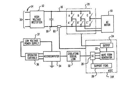
Figure 1 is a block diagram of an inverter and
control circuit according to the invention;
Figure 2 is a diagram of an ASIC for waveform
generation and inverter control at high voltage level
according to the invention;
Figure 3 is a diagram of AC motor field rotation
sectors;
~ Figure 4 is a vector diagram of motor phase
voltages for a single sector;
Figure 5 parts (a) through (d) are illustrations
of signals generated and state machine states in the
waveform generator according to the invention;
20~73~
ETC-023 26G0
Figure 6 is a functional diagram of the waveform
generator implemented on an ASIC chip according to the
invention;
Figure 7 parts (a) and (b) comprises a diagram of
the state machine logic for the waveform generator of
Figure 6, according to the invention;
Figure 8 parts (a) through (c) are illustrations
of signals generated and state machine states in the
waveform generator for over-modulation operation, according
to the invention; and
Figure 9 parts (a) and (b) are illustrations of
carrier signal and sector signals, respectively, for
synchronous operation.
DESCRIPTION OF THE INVENTION
OV~T T 8YSTEN: The diagram of Figure 1 shows the
overall system for controlling a three phase asynchronous
(induction) AC motor 10. A DC power source here depicted
as a rectifier 12 coupled to a three phase AC line 14
provides DC voltage on positive and negative DC busses 16
and 18. Of course single phase AC may be rectified as
well. The voltage on the busses 16 and 18 is typically
several hundred volts. The busses are not referenced to
ground and thus float with respect to ground. Typically
the negative bus is about 390 volts below ground. An
2~1732~
- 6
ETC-023 26G0
inverter 20 of conventional structure comprises a plurality
of transistor switches connected serially in pairs A-A',
B-B' and C-C' across the positive and negative busses and
each switch pair junction point is connected to an input of
the motor 10 to energize a phase of the motor.
The switching convention used here is that if
either switch of a pair is closed the other switch of the
pair must be open; thus A' means A-not and always has the
opposite state of A. An exception is imposed by an anti-
overlap function which may hold both switches open for aninstant during a switching interval to insure that they are
not both closed at any time. By selectively opening and
closing the switches the three phases of the motor 10 are
energized by many short pulses to create average current in
each phase appropriate to the desired motor operation.
OPTICAL I~OLATION: The trigger pulses for
operating the transistor switches of inverter 20 are
produced by a waveform generator 22 and coupled to the
inverter 20 via an output circuit 24. The waveform
generator 22, the output circuit 24, a serial communication
(SC) circuit 26 and other support functions 28 described
below are all part of a single ASIC chip 30 which is
referenced to the potential of the negative bus 18. An
isolating serial link 32 including two opto-isolators
2 ~ 2 2
,
ETC-023 26G0
couples signals between the serial communication circuit 26
and microprocessor logic or microcontroller 34 which is
referenced to ground potential and which generates signals
to control the operation of the waveform generator 22. A
conventional low voltage power supply 37 supports the
microcontroller 34 and controls 36. Operator controls 36
provide inputs to the microcontroller 34. The grounded
state of the logic allows control signals from external
hardware such as switches, potentiometers, relays,
programmable controllers, etc. to be directly connected to
this portion of the circuitry without concern for operator
or installer safety or the need for high voltage wiring.
Thus the microcontroller 34 and the operator controls
afford an interface between the operator and the waveform
generator 22 through the isolating link which protects both
the operator and the microcontroller from the high voltages
of the DC bus 18. The placement of the ASIC 30 in the high
voltage side allows the three negative power switching
devices A', B' and C' to be directly driven (the positive
switching devices being switched through simple level
shifting circuitry), and allows high switching frequencies
without the need for expensive opto-couplers or pulse
transformers. At the same time, the optical isolation
required for the serial link is neither difficult nor
expensive, particularly when the ASIC provides the high
2~ ~732~
-- 8 --
ETC-023 26G0
side serial communication circuitry and low common mode
dV/dt rates are observed. Bus current can be sensed by a
simple shunt resistor and voltage by resistive dividers,
not shown. Positive bus voltage and each phase voltage is
thus monitored. Average values of these analog signals are
converted to digital form and sent through the serial port
for control and readout purposes.
The ASIC 30 generates other control signals in
addition to the normal gating signals. It includes PWM
signal generators to provide analog references, and also
provides for an external analog to digital converter. It
communicates with the microcontroller 34 through a serial
port which can be optically coupled with low cost
components. The ASIC is programmed by the microcontroller
by means of several addressable eight bit registers.
Status information from the ASIC may be read by the
microcontroller in a similar manner.
ASIC: While several technology choices are
available, it is here preferred to use CMOS gate array
technology to form the ASIC. The ASIC is shown in Figure
2 and is divided into seven functional blocks. Each block
has a set of registers associated with it by which the
microcontroller establishes operating conditions or
monitors the state of the ASIC or its inputs. For clarity,
' . 2~73~
g
ETC-023 26GO
the signal busses interconnecting the blocks are not shown.
The serial communications block 26 is responsible
for transferring data between the ASIC 30 and the
microcontroller 34. It operates in an asynchronous mode,
and provides error checking. Address registers 38 in this
block point to the other registers in the chip. T h e
waveform generator 22 is the heart of the drive. It
accepts 16 bit values in three registers 40, 42 and 44 for
output frequency, carrier period, and duty cycle,
respectively. It also includes a ROM 46 embodying lookup
tables of reference voltage values and logic driven by the
register contents for addressing the look up tables and for
deriving pulse width modulated switching signals. The
waveform generator produces three output phase signals
based on a well defined algorithm which allows
over-modulation, current limit, and both synchronous and
asynchronous carrier types of operation. It calculates the
period of the output frequency at sixty degree intervals.
An output block 48 generates six gating signals
from the three phase signals produced by the waveform
generator 22. Its register 50 allows anti-overlap time to
be programmed. It responds to an external current limit
signal and to register bits which enable the output and
allow phase interchange for reversing the motor. Three
external fault signals and a current limit signal allow the
~73~
.
-- 10 --
ETC-023 26Go
fault block 52 to disable the drive and signal a fault to
the microcontroller 34 through the serial port. A maximum
current limit rate may be programmed. The fault block also
monitors the gating signals and stores the number of the
most recent gating signal to become active to allow
diagnostic information to be displayed by the
microcontroller.
A control block 54 provides additional external
inputs and outputs. It also contains registers which allow
the microcontroller to manipulate bit signals in other
blocks.
Analog input and output is provided by two
independent PWM signal generators and a parallel interface
to an A/D converter in an analog block 56. This allows the
microcontroller to monitor average bus current and to set
current limit and dynamic braking references.
A utility block 58 provides a crystal oscillator,
a watchdog timer, test circuitry, and a timing signal
generator.
In operation of the ASIC chip, signals from the
microcontroller are carried by the serial link 32 through
an opto-isolator to the serial communications block which
transfers the data to registers elsewhere on the chip
according to addresses in the incoming signal. The data
includes waveform information which is fed into the
~732~
-- 11 --
ETC-023 26G0
registers 40, 42 and 44 in the waveform generator 22.
These registers are updated frequently by the
microcontroller to continually control the waveform
produced. The output of the waveform generator 22 is
supplied to the output 48 which directly operates the
negative inverter switches and operates the positive
inverter switches through a simple level shifting circuit.
An external current sensor 60 responsive to average bus
current feeds a current signal to the analog circuit 56.
Whenever the current exceeds a set limit, a limit signal is
sent to the fault block 52, the control block 54 and the
waveform generator. If this current limit occurs too
often, the fault block issues a fault signal.
Three other external inputs to the fault block as
well as a watch dog signal can trigger a fault signal. The
effect of the fault signal is to shut down the output
circuit 48 to terminate inverter operation, and to set a
fault flag in a status register in the control block 54.
For diagnostic purposes, the fault block also latches into
a register a code representing the type of fault which
occurred and the last switch signal issued. The
microcontroller regularly queries the status register and
if a fault is found it also queries the fault block
register to determine the cause of the fault. A watch dog
circuit in the utility block 58 is reset each time the
- -12- ~c 20~73Z ~
microcontroller queries the status register. If the query
fails to occur within a preset time period indicative of
microcontroller or serial link failure, the watch dog circuit
signals the fault block which issues a fault signal to turn
off the inverter.
Thus the ASIC chip provides a self sufficient control
circuit able to function at the voltage level of the inverter
bus and requiring only control data from the microcontroller
which can readily be supplied over the serial link which is
serviced by a relatively inexpensive optical coupler.
WAVEFORM ALGORITHM: The paper "Analysis and Realization of a
Pulse Width Modulator Based on Voltage Space Vectors" Van der
Broeck et al., Conf. Rec. 1986 Annual Meeting IEEE Ind.
Appl. Soc., pp244-251 describes a PWM technique for energizing
a three phase AC machine with minimal distortion yet allows
significant over-modulation. The full 360 revolution of the
motor is divided into six 60~ sectors I through VI as shown in
Figure 3. The currents in the three phases of the motor
required to establish the rotating field of the stator in one
sector is determined by sequentially applying the two
available voltages Ul and U2 on the DC bus to two phases and
varying the time interval
~Q~73,~
- 13 -
ETC-023 26G0
of each phase energization in a proportion to achieve the
correct vector angle A at any instant (Figure 4) and then
progressively changing the angle with time to effect the
field rotation. For example, the voltage U1 is first
applied by actuating switches A, B' and C' for a short
interval and then actuating switches A, B and C' to apply
voltage U2 for another interval, the ratio of the two
periods determining the effective vector angle of the
field. A feature of the technique is that the pulses are
applied in symmetrical groups to reduce harmonics. After
an interval of no voltage, the voltage U2 is again applied
followed by the voltage Ul. The angle of the vector is
correctly calculated by varying one of the energization
intervals according to the function sin (A) and the other
interval according to sin (60-A).
The magnitude of the current is adjusted by using
a variable duty cycle, that is, opening or closing all the
positive switches so that no voltage is applied for a time.
The interval of no voltage does not affect the angle, only
the magnitude. When any sector has been completed the
process is repeated for the ensuing sector, a different
switch pattern being used to energize the phases
appropriate for that sector. Thus pulse width modulation
effects machine control where adjacent pulses actuate
different switches for different intervals to create a
3 2 ~
- 14 -
ETC-023 26Go
rotating field vector and the pulse duty cycle determines
-the field strength or current in accordance with desired
motor torque.
The algorithm employs a carrier frequency (lkHz to
15kHZ) which is much greater than the machine frequency.
It is assumed that the carrier is fixed for a particular
application as a matter of design. Each carrier half
period is normally divided into three states, as
illustrated in Figure 5, the first two states being used to
apply the two voltages Ul and U2 and the third state is
used for the zero voltage (U3) interval. The periods of
time spent in the first two states are determined by the
values sin (A) and sin~60-A) which are stored in a look up
table and which repeat at 60~ intervals. These sine
functions are compared to a free running counter whose rate
of increment is inversely proportional to desired voltage
amplitude.
WAVEFORN ~N~R~TOR: Referring to Figure 6 the
waveform algorithm is implemented in the ASIC chip. It is
necessary for the microcontroller 34 to establish the
desired motor operation by providing via the serial data
link the machine frequency which is stored in the frequency
register 40, the carrier period which is stored in the
carrier register 44, and the duty cycle which is a quantity
2~73~
- 15 -
ETC-023 26G0
related to carrier period divided by duty cycle and is
stored in the duty slope register 42. The look up table
for the two sine functions is stored in ROM 46. With this
information, the waveform generator is able to output the
required switching commands.
A stator angle calculator includes the frequency
register 40, an adder 70, and an angle register 72 clocked
at a fixed frequency. The angle register 72 is
continuously incremented by the value of the freguency
register 40. A portion of the angle register represents
the ROM address of the angle A which is advanced to a latch
74 at the beginning of each carrier cycle as indicated in
Figure S(d). The appropriate sine value is loaded from the
table into a shape register 76 via a data selector 78.
O~L~uLs 82 from a state machine 80, described below,
determine whether sin A or sin (60-A) is loaded into the
shape register as well as the time of loading each value.
A state machine output 84 also determines when a new angle
may be latched into the ROM address.
The carrier register 44 is coupled to a carrier
counter 86 which is loaded with the register 44 value and
counts down, reloads and counts down again to produce the
ramps of Figure 5(c). When the counter 86 reaches zero it
produces an output on line 88 which feeds into the state
machine 80.
~7~2~
- 16 -
ETC-023 26G0
The duty cycle generator is a variable slope ramp
generator. It is constructed from the duty slope register
42, an adder 90 and a duty cycle register 92 which serves
as an accumulator. The upper bits of the register are fed
S to a comparator 94 for comparison to a timing value. The
duty cycle register 92 is clocked at a fixed rate via line
93 to add the slope register 42 contents to register 92
thereby creating a ramp shown by the broken lines in Figure
5(a). The ramp slope is thus determined by the contents of
- the duty slope register 42. As shown in Figure 5, when the
ramp reaches the sine value the state changes and the ramp
is reset to zero. This is accomplished by the comparator
94 which produces an output on line 96 to the state machine
when the duty cycle register 92 count is greater than the
shape register 76 value. The state machine, in turn,
produces a reset signal to the duty cycle register 92 on
line 98. The reset signal can be used to hold the duty
cycle register count at zero.
Pulse Director: A pulse director 100 determines
from information on the present sector and a built-in
table, which switches should be turned on for each vector
and issues switch command signals on three output lines
102. The state machine 80 supplies the vector and timing
information and a sector register 104 provides the sector
20~732~
- 17 -
ETC-023 26G0
information. The sector register 104 is a divide by six
counter which is incremented by an overflow signal from the
angle register 72 on line 105 whenever a 600 sector is
completed. A current limit signal to the pulse director
causes the pulse director 100 to gate the output signals to
the same polarity to remove voltage from the motor. The
pulse director also turns off a gate 101 to remove clock
signals from the registers 72 and 92 and the counter 86 to
freeze the action of the waveform generator as long as the
current limit signal lasts.
The overflow or sector complete signal on line 105
from the angle register 72 also provides inputs to a period
register 106 and a counter 108 which is clocked at a
constant rate. At the end of each sector the counter value
is loaded into the register 106 and the counter 108 is
reset. Thus the period register holds a value which is a
measure of the period and is useq for feedback information
to the microcontroller 34 to apprise the microcontroller of
the period status in the event of an interruption by a
current limit signal.
~ tate Machine: The state machine 80 drives and
coordinates the other components of the waveform generator.
It is a logic circuit formed in the ASIC and is dedicated
to the orderly operation of the generator. The chart of
Figure 7 illustrates the sequence of operation. Reference
7 ~
18
ETC-023 26G0
numerals in angle brackets <nn> refer to the numerals of
blocks functions being described. In conjunction with
Figure 5, the timing and interaction of the several
register outputs is readily under stood. Assuming that the
machine enters state 0 at power up, the duty cycle register
is held in reset mode <110>. When the carrier count is
complete <112>, the row pointer is updated (via line 84),
and sin(60-A) is loaded into the shape register 76 <114>.
Then a transition is made to 1 state where the Ul vector is
applied and the duty cycle register is released <116>. If
the carrier count is not complete <118> and the duty
register value reaches the sine value in the shape register
<120>, sin(A) is loaded into the shape register and the
duty cycle register is reset <122> and the transition to 2
state is made and the U2 vector is applied <124>. Again,
if the carrier count is not complete <126> and the duty
cycle register value reaches the shape register value
<128>, the 3 state is entered <130> where the U3 vector
obtains (no motor voltage) and the duty cycle register is
held in reset mode. Then, when the carrier count is
complete <132>, sin(a) is loaded into the shape register
<134> and the 4 state is entered <136> where the U2 vector
is again applied and the duty cycle register is reset and
released. If the carrier count is not completed <138> and
the duty cycle register count reaches the shape register
20~3~
-- 19
ETC-023 26G0
value <140>, sin(60-A) is loaded .into the shape register
<142> and the transition to 5 state is made <144> where the
vector Ul is applied and the duty cycle register is reset.
If the carrier count is not complete <146> and the duty
cycle register reaches the shape register value <148>, the
transition to o state is made <110> where the cycle
repeats.
This process is the regular progression of the
state machine which sequences through all six states as
shown in Figure 5 and applies up to 100% modulation. At
that point the 3 state and the 0 state are reduced to zero
time period and, at over-modulation, the 2 state is
truncated by the carrier count completion prior to the duty
cycle register count reaching the shape register value as
shown in Figure 8. To assure that the 2 state and the 4
state have equal periods to maintain symmetry, the value of
the duty cycle register is loaded into the shape register
as indicated at Figure 8(a). This is accomplished by the
data selector 78 which is triggered by the state machine to
load data from the duty cycle register 92 instead of from
the table 46. Then during the 4 state the duty cycle
register will reach the shape register value at the correct
time. In Figure 7, when the carrier count is complete at
block 126, the duty cycle register is loaded into the shape
register at block 150 and the state goes directly to 4
j 3 2 ~
- 20 -
ETC-023 26G0
state. At the end of 5 state <144> the carrier count is
complete <146> and the 0 state is bypassed and the next
operation is block 114 which loads updated information into
the registers for the next cycle starting at 1 state.
In the limiting over-modulation condition the
state machine toggles between 1 state and 5 state to
produce a square wave input to the motor. In Figure 7, if
the carrier count is completed while in 1 state <118>, the
state machine goes to block 142 to load the shape register
and then to block 144 to enter 5 state. Then if the
carrier count is completed <146> the logic flows to block
114 to prepare for the 1 state.
The operation of the waveform generator is usually
asynchronous but it is sometimes desirable, particularly at
high stator frequency, to operate synchronously wherein the
carrier frequency is an integral multiple of stator
frequency. A switch 160 under control of the
microcontroller 34 can be closed to command synchronous
operation. The switch connects the sector completion
signal on line 105 to the carrier counter 86 to force a
reset of the counter and to issue a carrier count complete
signal. The microcontroller 34 sets stator frequency and
carrier period values which approximate synchronous
conditions so that at the end of a 600 sector the carrier
- 20~ ~ ~2~
- 21 -
ETC-023 26G0
count is close to zero as shown in Figure 9. When the
sector completion signal is issued on line 105 any error in
the carrier count is removed by resetting the carrier count
to zero and the state machine to 1 state via the carrier
count completion signal and the new 600 sector is begun.
As shown in Figure 9(a) an approximately even number of
carrier half cycles occur between the sector completion
signals on line 105 shown in part (b) of Figure 9. The
last half cycle is truncated at the end of the sector.
It will be seen that the waveform generator is
able to produce a PWM output for controlling the inverter
switches in a manner to produce a rotating field having a
frequency dependent on the contents of the frequency
register and a magnitude dependent on the contents of the
duty slope register. The switching pulses are produced at
a rate determined by the contents of the carrier register.
Generally four pulses per period are produced unless a
square wave is produced at two pulses per period. The
waveform generator can smoothly change into and out of an
over-modulation condition and can switch between
synchronous and asynchronous operation. The
microcontroller is in control of the waveform generator at
all times except when a current limit is detected or a
fault is detected in which case the generator function is
frozen for a time or stopped altogether. The register
~ ~0473~
- 22 -
ETC-023 26G0
contents can be updated at any time by the microcontroller.
The embodiments of the invention in which an
exclusive property or privilege is claimed are defined as
follows: